Tin Whisker Growth Suppression Using NiO Sublayers Fabricated by Dip Coating
by
 ,
,
Jacob D. Buchanan
1, 
Vamsi Borra
1,2,* ,
,
Md Maidul Islam
1,
Daniel G. Georgiev
1 and
Srikanth Itapu
1,3 1
Department of Electrical Engineering and Computer Science, University of Toledo, Toledo, OH 43606, USA
2
Electrical and Computer Engineering Program, Rayen School of Engineering, Youngstown State University, Youngstown, OH 44555, USA
3
Department of Electronics and Communication Engineering, Alliance College of Engineering and Design, Alliance University, Bengaluru 562106, India
*
Author to whom correspondence should be addressed.
Condens. Matter 2022, 7(1), 7; https://0-doi-org.brum.beds.ac.uk/10.3390/condmat7010007
Submission received: 9 October 2021
/
Revised: 23 November 2021
/
Accepted: 28 December 2021
/
Published: 6 January 2022
(This article belongs to the Special Issue Electronic Materials and Devices 2021)
Abstract
:Whiskers are small crystalline growths, which can grow from certain metals or alloys. Reaching up to several millimeters long, whiskers have the potential to cause device failures due to short circuits and contamination by debris. Tin (Sn) is one such metal that is particularly prone to whisker development. Until the 2006 RoHS Initiative, lead (Pb) was added to tin in small amounts (up to 2%) to greatly reduce the growth of whiskers. Since then, however, industry has switched to lead-free tin solders and coatings, and the issue of whisker growth on tin has attracted new interest. A reactive-sputtering-deposited nickel oxide sublayer was shown recently to strongly suppress the growth of whiskers from an overlaying tin layer. This paper reports on using nickel oxide films, obtained by a sol–gel dip coating method, as whisker suppressing sublayers. The proposed method is simple, low-cost, and can easily be scaled up for manufacturing purposes. The properties of the sol–gel deposited nickel oxide film were examined using SEM, EDS, and Raman spectroscopy. Samples containing the nickel oxide sublayer were observed through SEM periodically over several months to examine the surfaces for whisker development, and the results show that such layers can be very effective in suppressing whisker growth.
Keywords:
whiskers; electronic materials; whisker mitigation; failures; NiO; nickel oxide; Sn; reliability1. Introduction
Metal whiskers are long, thin, hair-like structures, which grow on the surfaces of thin films of certain metals and alloys. They have been observed growing on several elemental metals including Sn [1,2,3], Zn [4,5], Pb [6], and Cd [5], as well as metal alloys such as bronze and brass [6]. As tin is used extensively in the electronics industry, often alongside copper, the growth of whiskers on many commercial devices is a real concern. Although whiskers have been studied for several decades [3,7], the mechanisms of their nucleation and growth are still not fully understood [8,9,10,11,12,13,14,15,16,17].
There are several ways in which whiskers can lead to device failures [3,8,18]. These include both permanent and transient short circuits [2], contamination by debris, and metal vapor arcing. Such failures have been documented in the telecom, military, aerospace [19], energy, and medical industries since the 1940s [3,18]. Traditionally, small amounts of lead were added to tin to suppress the growth of whiskers [18]. This was the standard preventative measure until the passage of the RoHS Directive [15,20]. Effective 1 July 2006, this directive prevents the sale of products containing lead within the European Union (which represents a market large enough to influence industry practices around the globe). Because of this, new mitigation methods are required to prevent device failures brought on by the use of pure tin in electronics.
Alloying is a known (although not well understood) method of whisker growth mitigation. In addition to the conventional approach of adding Pb to Sn, alloying Bi or In with Sn has shown potential as well [21,22]. Conformal coatings represent another popular approach. Such coatings are typically made of a polymer and are applied postproduction, making them affordable and easy to implement. In some cases, they have been shown to prevent the growth of whiskers [1]. However, there is evidence that whiskers can grow into these coatings and may even become long enough to penetrate them [19,23].
Addition of a sublayer underneath the tin film is another whisker suppression method. This sublayer has the intended effect of reducing or eliminating whiskers on the overlying tin surface. The mechanism through which this approach can lead to whisker growth suppression is considered to be based on creating a barrier to block diffusion [24,25] or reducing stress in the tin layer [25]. These sublayers can be made of metals and alloys such as nickel [24,26], nickel/gold [25], or thin film metallic glasses [27].
The recently proposed electrostatic theory of metal whisker growth [28,29,30,31,32] has motivated the idea of using a semiconducting sublayer (NiO in this case) to mitigate whisker formation. This work is motivated in part by the fact that the Ni sublayers have indeed shown some effect on whisker growth when compared with the Sn-coatings without a sublayer [33], as an extension of our previous work [34]. As previously demonstrated [34], sputtering NiO has shown promising results. However, sputtering is not the ideal method to be deployed for the commercial scale manufacturing [35]. Conversely, electroplating is well studied and can be adapted for industrial settings. The contact potential at a tin–copper interface contributes to an electric field, which may drive whisker growth [36,37,38]. An additional sublayer can split this contact potential at the Sn–NiO–Cu interfaces and, thus, decrease any local electric fields [34]. Nickel oxide was found to be particularly effective as such a semiconducting sublayer material. A sputtering-deposited sublayer of nickel oxide between copper and tin has been shown to completely prevent the growth of tin whiskers [34]. Being a vacuum method, this would be too costly or too inefficient to scale up for use in industrial manufacturing. Nickel oxide films have also been created using sol–gel, thermal oxidation, electron beam evaporation, and chemical bath deposition methods. Sol–gel processes are inexpensive, require relatively simple equipment, can be performed in atmospheric air, can be scaled up efficiently, and allow for a great degree of control over the film structure [39,40,41,42,43]. This makes sol–gel dip coating an appealing method for deposition of whisker-mitigating sublayers, and this work examines its suitability and effectiveness.
2. Experimental Methods
2.1. Substrate Preparation
Glass microscope slides were cleaned using a standard procedure. The slides were placed into a glass dish containing a solution of Micro-90 detergent and water. This dish was placed into an ultrasonic bath and sonicated for 20 min. Afterwards, the glass slides were rinsed with deionized water and dried with clean compressed air. This process of sonication and drying was repeated twice more: first using ethanol (95%, DeconTM Labs, King of Prussia, PA, USA) as a solvent and then using acetone (99.8%, Fisher, Fair Lawn, NJ, USA).
A copper film was deposited onto the clean glass slides by RF sputtering. The working gas used was argon at a working pressure of about 10 mTorr at an RF power of 100 W. A smooth Cu film with a thickness of 300 nm was deposited at a rate of 0.4 nm/s.
2.2. Sol–Gel Solution
The solution [44] was prepared by dissolving 5.10 g of nickel 2-ethylhexanoate (~15% Ni, American Elements, Los Angeles, CA, USA) in 2-propanol (99.9%, Fisher), diluted to a volume of 30 mL. The mixture was covered and stirred for two hours prior to deposition, and the resulting solution was transparent and greenish in color. The concentration of nickel in the solution was 0.44 M.
2.3. Dip Coating Deposition
The dip coating process was carried out using a NIMA Dip Coater (NIMA DC Multi 8). The substrate-lowering speed was set to the maximum value of 280 mm/min. After reaching the lowest point, the substrate holder paused for 5 s. Then, the substrate was withdrawn from the solution at a rate of 1 mm/s. When the substrate was completely removed from the solution but still within the vapors in the beaker, the substrate holder was stopped for five minutes. This additional drying step helps prevent the film from cracking when abruptly exposed to air [45]. The samples were then placed in a furnace preheated to 100 °C. At this temperature, they were dried for 10 min in air. Afterwards, they were calcinated in the same furnace at 350 °C for 10 min.
2.4. Tin Deposition
A layer of tin was deposited on the samples by thermal evaporation. In the evaporator (Denton, Model#DV-502A), tin pellets were heated in a tungsten boat (Kurt J. Lesker, Jefferson Hills, PA, USA, Part#EVS6005W) until molten. The applied current during deposition was 110 A. The resulting tin film was 500 nm thick and was deposited at a rate of 0.25 nm/s.
2.5. Characterization Methods
Both EDS and Raman spectroscopy were used to analyze the chemical composition and structure of the prepared films. EDS was performed on the exposed nickel oxide layer and on fully-formed samples with an outer coating of tin. Several regions were examined, and an average of the collected values was taken. Raman spectroscopy was performed only on the exposed nickel oxide films using a JY Horiba LabRAM confocal Raman spectrometer with 632.8 nm laser excitation (resolution of 0.16 cm−1 at 632.8 nm with an 1800 g/mm grating).
The long-term examination of whisker growth was carried out using SEM. Samples were imaged shortly after their fabrication and every month thereafter. Samples containing the nickel oxide sublayer and those without it (deemed control samples) were created and examined synchronously and simultaneously. In doing so, the nucleation and progression of growth of whiskers was recorded.
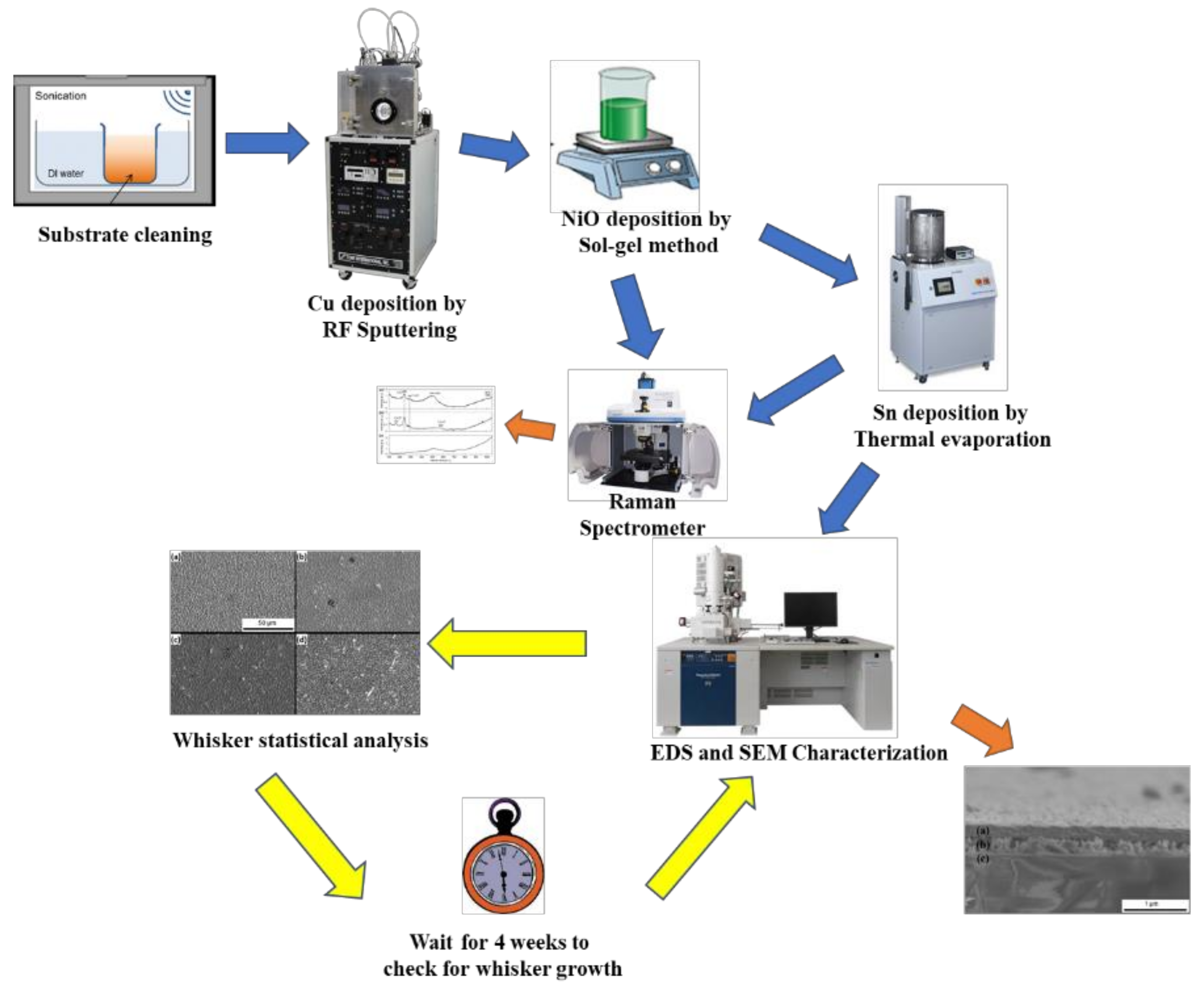
As a standard, 40 SEM images were captured on each sample each time they were investigated. The magnification used for each sample was held constant at 1000. Each image had an area 140 µm by 85 µm, or 1.19 × 10⁻² mm2. With 40 of these images, the total examined area each time was 0.476 mm2. Within this equivalent area, a count was kept of each whisker at least 5 µm in length. The sample preparation and characterization steps are illustrated in Figure 1.
3. Results and Discussion
3.1. Characterization of the NiO Films
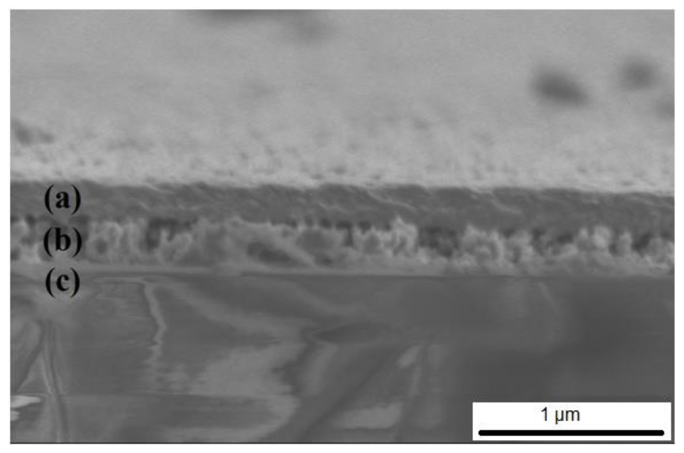
The thickness of the NiO films deposited by dip coating was measured by cross-sectional SEM. A glass slide (precoated with Cu) was coated using the dip coating procedure detailed above but modified for five successive dip coating cycles. Then, the glass slide was scored with a diamond-tipped glass cutter and fractured. The profile of the film was then imaged by SEM, and the thickness of the film was measured to be 300 nm (see Figure 2). Assuming an equal thickness deposited during each dip coating cycle, the thickness of the single-cycle dip coating cycle was taken to be 60 nm.
The chemical composition of the film was first checked using EDS. The values obtained were from the exposed sublayer on a substrate of sputtered copper on glass. An accelerating voltage of 10 kV was used. The results are shown in Table 1 below.
The elements with significant contributions were carbon, oxygen, silicon, nickel, and copper. Additionally, calcium and aluminum were found to be present in trace amounts (less than 1%). The solution which formed the nickel oxide layer contained carbon, oxygen, nickel, and hydrogen. However, hydrogen could not be detected by EDS techniques; therefore, it was absent. The significant amount of copper detected was entirely from the underlying sputtered copper film. The silicon and a portion of the oxygen content were due to the glass slide substrate. Our substrates were made of soda-lime glass which was composed of a mix of silicon dioxide, sodium carbonate, calcium oxide, magnesium oxide, and aluminum oxide. An accelerating voltage of 26 kV was used for the sample’s area where tin was deposited as it required a larger interaction volume for accurate EDS measurement. The results are shown in Table 2. It can be noticed that as the quantity of tin increased, the copper signal became weaker. This is to be expected since the interaction volume of the beam remained largely the same.
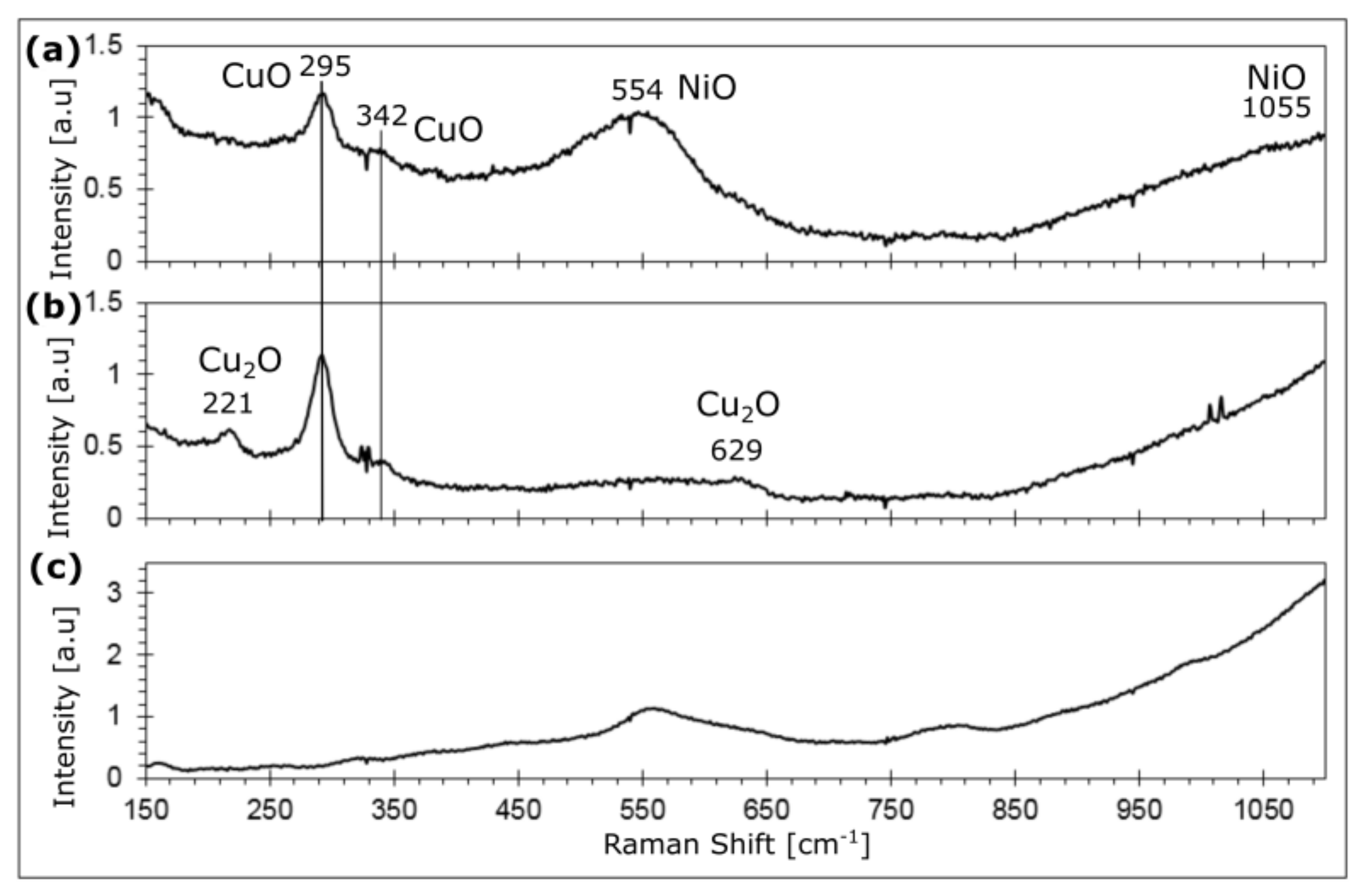
Raman spectroscopy was used to verify the existence of NiO bonds in the layers. The Raman measurements were carried out on exposed nickel oxide layers only, due to the limitations of this method in penetrating a metal layer (i.e., the top tin film). Spectra obtained were from samples, which were cycled five times during the dip coating process, which helped to increase the sensitivity of the measurements. Representative Raman spectra are shown in Figure 3.
Nickel oxide, in the form of NiO, was clearly present in the dip-coated film according to the spectrum (Figure 3a), obtained from the part of the sample, which was dip coated. The peaks at 554 cm−1 and 1055 cm−1 were consistent with NiO prepared using similar methods [46,47,48]. Other peaks were also present, two of which can be seen in the spectrum taken from the part of the sample, which was not dip coated. The literature suggests that the peaks located at 295 cm−1 and 342 cm−1 (common to both spectra and shown with vertical lines in the figure) belong to copper oxide CuO [46,49,50] and the peaks at 221 cm−1 and 629 cm−1 can be attributed to the Cu2O phase [50]. This indicates that a mixed-phase copper oxide was present underneath the nickel oxide film.
3.2. Sn Whisker Growth
Two sets of four samples each were prepared and examined over several months to record whisker growth. Within these sets, there were two samples (Sample #1 (S1) and Sample #2 (S2)) containing the sol–gel-deposited sublayer and two lacking it (C #1 (C1) and Control #2 (C2)). All parameters used to prepare corresponding samples across both sets were kept the same; the only difference was the time at which they were made. The total number of whiskers found across all SEM images that week along with density calculations are provided in Table 3.
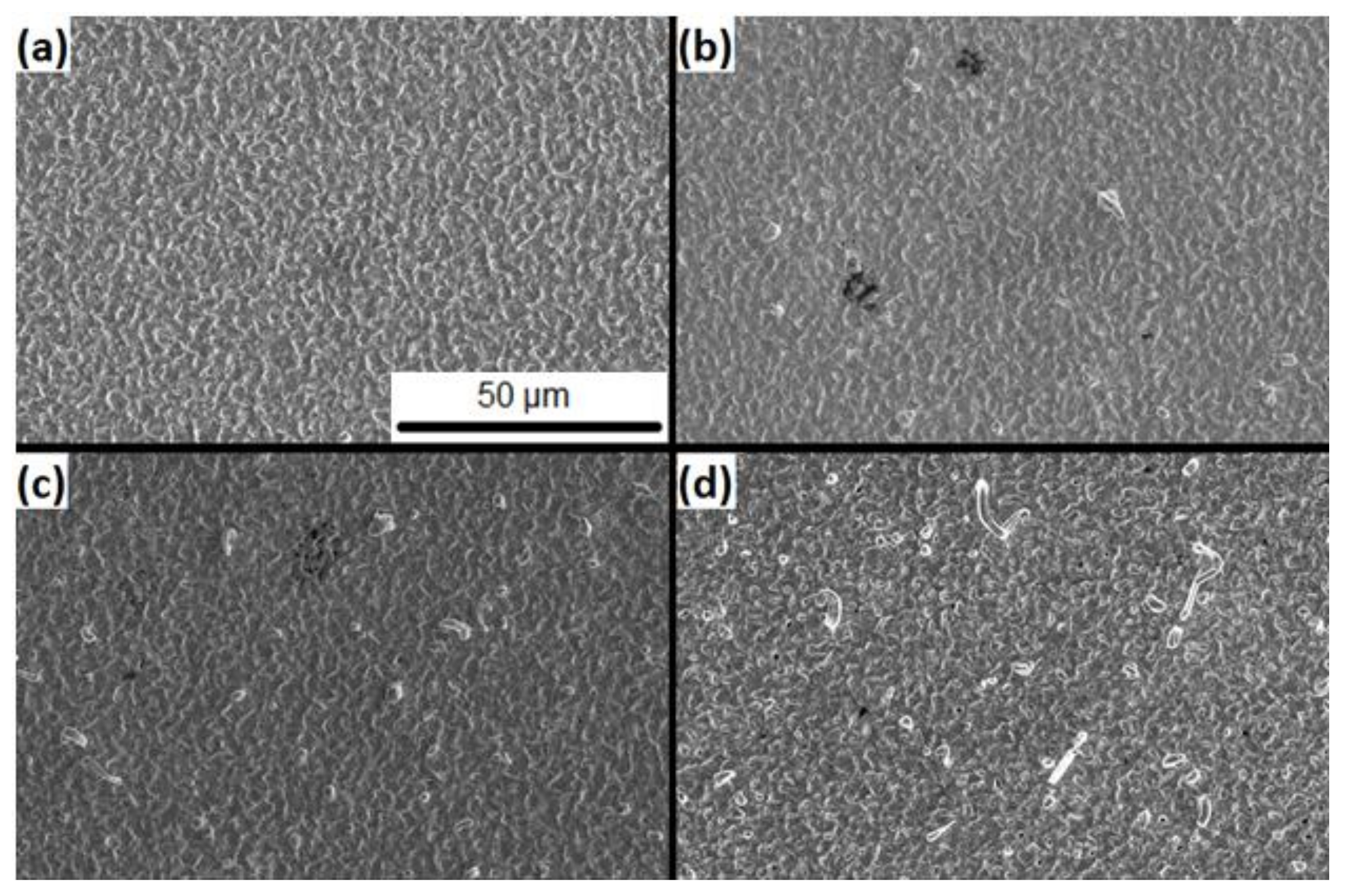
The whisker count data show that the number of whiskers increased as a function of time (almost linearly) on the samples without the nickel oxide sublayer. After four months of aging, these controls showed an average density of 272 whiskers per mm2. In contrast, the samples, which featured a nickel oxide sublayer contained no whiskers. Representative SEM images of one NiO sublayer sample and one control sample are provided in Figure 4 and Figure 5 respectively.
According to the electrostatic theory of whisker growth [28], the existence of substantial electric fields can drive the formation of metal whiskers. These electric fields are intrinsic to the material or even can be externally applied. The intrinsic uncompensated electric charges are generally due to the interfaces, grain boundaries, local variations in chemical compositions, and others [28,49]. For this work, a simplified electrostatic picture, based on the difference between the work functions of Sn and Cu is considered. Here, the difference was calculated to be ~0.53 eV [50,51], which was a significant built-in electric field at the Sn/Cu interface when the two materials did not intermix. In the case of diffusion of Cu into Sn, specifically considering the influence from the grain boundaries, it would result in a drastically nonuniform [52] lateral distribution of Cu, whose local concentration will fluctuate from nearly zero to almost 100 percent. These events would lead to the corresponding local variations in work function of the order of the above estimated 0.53 eV. Subsequently the free electrons would redistribute themselves in such a way as to minimize the system free energy, which would result in the electric charge distribution becoming laterally nonuniform. This inhomogeneous ‘electric patch’ structure reaching to the film surface is a major requirement of the electrostatic theory of whisker growth. A similar interpretation can explain whisker suppression in the Sn/NiO/Cu case if we assume that the NiO layer blocks Cu diffusion, thus, suppressing electric nonuniformities and mitigating whisker growth. In addition, it is to be noted that the contact potential between Sn and NiO, which is the approximate work function difference between the two materials, can be closer to ~0.4 eV or even less. This approximation was obtained from the electron affinity [53] and band gap [35,54] values for NiO assuming almost degenerate p-type NiO [35].
4. Conclusions
Our results support the idea of using a nickel oxide sublayer, deposited by a sol–gel dip coating method, as a method for suppressing whisker growth. Over the duration of this observance, it was found that samples containing this sublayer grew practically no whiskers. Meanwhile, control samples without the sublayer grew whiskers on the order of a couple hundred per square millimeter. Clearly, this work provides very strong evidence that low-cost dip-coating obtained semiconducting NiO sublayers can be used as an effective whisker growth mitigation method, which is expected to be of substantial importance to various industrial applications.
Author Contributions
Conceptualization, D.G.G. and V.B.; methodology, J.D.B.; software, M.M.I.; validation, V.B., D.G.G. and J.D.B.; formal analysis, J.D.B.; investigation, J.D.B. and V.B.; resources, D.G.G.; data curation, J.D.B., V.B., S.I. and M.M.I.; writing—original draft preparation, J.D.B.; writing—review and editing V.B., D.G.G. and S.I.; visualization, J.D.B.; supervision, D.G.G. and V.B.; project administration, D.G.G. and V.B.; funding acquisition, D.G.G. All authors have read and agreed to the published version of the manuscript.
Funding
This research received no external funding.
Institutional Review Board Statement
Not applicable.
Informed Consent Statement
Not applicable.
Data Availability Statement
Not applicable.
Acknowledgments
The authors would like to acknowledge helpful discussions with V. Karpov (University of Toledo, Department of Physics and Astronomy) as well as technical help and support by the University of Toledo’s Wright Center for Photovoltaics Innovation and Commercialization (PVIC) and particularly the research group of R. Ellingson. The SEM and Raman characterization work was performed at the University of Toledo’s Center of Materials and Sensors Characterization (CMSC).
Conflicts of Interest
The authors declare no conflict of interest.
References
- McDowell, M. Tin whiskers: A case study. In Proceedings of the 1993 IEEE Aerospace Applications Conference Digest, Steamboat Springs, CO, USA, 31 January 1993. [Google Scholar]
- Stupian, G.W. Tin Whiskers in Electronic Circuits; Aerospace Corporation: EL Segundo, CA, USA, 1992. [Google Scholar]
- Leidecker, H.; Brusse, J. Tin Whiskers: A History of Documented Electrical System Failures. 2006. Available online: https://ntrs.nasa.gov/citations/20060028088 (accessed on 9 October 2021).
- Coleman, R.; Sears, G. Growth of zinc whiskers. Acta Met. 1957, 5, 131–136. [Google Scholar] [CrossRef]
- Coleman, R.V.; Price, B.; Cabrera, N. Slip of Zinc and Cadmium Whiskers. J. Appl. Phys. 1957, 28, 1360–1361. [Google Scholar] [CrossRef]
- Sun, Z.; Hashimoto, H.; Barsoum, M.W. On the effect of environment on spontaneous growth of lead whiskers from commercial brasses at room temperature. Acta Mater. 2007, 55, 3387–3396. [Google Scholar] [CrossRef]
- Compton, K.G.; Mendizza, A.; Arnold, S.M. Filamentary Growths on Metal Surfaces–“Whiskers”. Corrosion 1951, 7, 327–334. [Google Scholar] [CrossRef]
- Zhang, P.; Zhang, Y.; Sun, Z. Spontaneous Growth of Metal Whiskers on Surfaces of Solids: A Review. J. Mater. Sci. Technol. 2015, 31, 675–698. [Google Scholar] [CrossRef]
- Lee, B.-Z.; Lee, D. Spontaneous growth mechanism of tin whiskers. Acta Mater. 1998, 46, 3701–3714. [Google Scholar] [CrossRef]
- Barsoum, M.W.; Hoffman, E.N.; Doherty, R.D.; Gupta, S.; Zavaliangos, A. Driving Force and Mechanism for Spontaneous Metal Whisker Formation. Phys. Rev. Lett. 2004, 93, 206104. [Google Scholar] [CrossRef] [PubMed]
- Murakami, K.; Hino, M.; Takamizawa, M.; Nakai, K. Mechanism of generation and growth of whiskers on tin electroplating. Mater. Trans. 2008, 49, 2829. [Google Scholar] [CrossRef]
- Vianco, P.T.; Rejent, J.A. Dynamic Recrystallization (DRX) as the Mechanism for Sn Whisker Development. Part I: A Model. J. Electron. Mater. 2009, 38, 1815–1825. [Google Scholar] [CrossRef] [Green Version]
- Crandall, E.R. Factors Governing Tin Whisker Growth; Springer International Publishing: Cham, Switzerland, 2013. [Google Scholar]
- Smetana, J. Theory of Tin Whisker Growth: “The End Game”. IEEE Trans. Electron. Packag. Manuf. 2007, 30, 11–22. [Google Scholar] [CrossRef]
- Chuang, T.; Lin, H.; Chi, C. Rapid growth of tin whiskers on the surface of Sn–6.6Lu alloy. Scr. Mater. 2007, 56, 45–48. [Google Scholar] [CrossRef]
- Chen, K.; Wilcox, G.D. Observations of the Spontaneous Growth of Tin Whiskers on Tin-Manganese Alloy Electrodeposits. Phys. Rev. Lett. 2005, 94, 066104. [Google Scholar] [CrossRef] [PubMed]
- Brusse, J.; Ewell, G.; Siplon, J. Tin whiskers: Attributes and mitigation. Cart. Eur. 2002, 16, 221–233. [Google Scholar]
- Brusse, J.A.; Ewell, G.J.; Siplon, J.P. Tin Whiskers: Attributes and Mitigation. In Proceedings of the 22nd Capacitor and Resistor Technology Symposium, New Orleans, LA, USA, 25–29 March 2002; pp. 67–80. [Google Scholar]
- Kadesch, J.S.; Brusse, J. The Continuing Dangers of Tin Whiskers and Attempts to Control Them with Conformal Coating. NASA EEE Links Newsletter. 2001. Available online: https://nepp.nasa.gov/whisker/reference/tech_papers/kadesch2001-article-dangers-of-tin-whiskers-and-conformal-coat-study.pdf (accessed on 4 January 2022).
- 2021 RoHS Compliance Guide: Regulations, 10 Substances, Exemptions. Available online: https://www.rohsguide.com/ (accessed on 9 October 2021).
- Jo, J.-L.; Nagao, S.; Hamasaki, K.; Tsujimoto, M.; Sugahara, T.; Suganuma, K. Mitigation of Sn Whisker Growth by Small Bi Additions. J. Electron. Mater. 2014, 43, 1–8. [Google Scholar] [CrossRef] [Green Version]
- Majumdar, B.S.; Dutta, I.; Bhassyvasantha, S.; Das Mahapatra, S. Recent Advances in Mitigation of Whiskers from Electroplated Tin. JOM 2019, 72, 906–917. [Google Scholar] [CrossRef] [Green Version]
- Kadesch, J.S.; Leidecker, H.; Day, J.H. Effects of conformal coat on tin whisker growth. In Proceedings of the Institute of Managed Account Professionals Conference, Dearborn, MI, USA, 1–3 October 2000. [Google Scholar]
- Dimitrovska, A.; Kovacevic, R. Mitigation of Sn Whisker Growth by Composite Ni/Sn Plating. J. Electron. Mater. 2009, 38, 2516–2524. [Google Scholar] [CrossRef]
- Skwarek, A.; Pluska, M.; Ratajczak, J.; Czerwinski, A.; Witek, K.; Szwagierczak, D. Analysis of tin whisker growth on lead-free alloys with Ni presence under thermal shock stress. Mater. Sci. Eng. B 2011, 176, 352–357. [Google Scholar] [CrossRef]
- Schetty, R. Minimization of tin whisker formation for lead-free electronics finishing. Circuit World 2001, 27, 17–20. [Google Scholar] [CrossRef]
- Diyatmika, I.M.W.; Chu, J.P.; Yen, Y.W.; Hsueh, C.H. Sn whisker mitigation by a thin metallic-glass underlayer in Cu-Sn. Appl. Phys. Lett. 2013, 103, 241912. [Google Scholar] [CrossRef]
- Karpov, V.G. Electrostatic Theory of Metal Whiskers. Phys. Rev. Appl. 2014, 1, 044001. [Google Scholar] [CrossRef] [Green Version]
- Borra, V.; Georgiev, D.G.; Karpov, V.G.; Shvydka, D. Microscopic Structure of Metal Whiskers. Phys. Rev. Appl. 2018, 9, 054029. [Google Scholar] [CrossRef] [Green Version]
- Borra, V.S.V. Whiskers: The Role of Electric Fields in the Formation Mechanism and Methods for Whisker Growth Mitigation. University of Toledo. 2017. Available online: http://rave.ohiolink.edu/etdc/view?acc_num=toledo1513381893591481 (accessed on 9 October 2021).
- Borra, V.; Georgiev, D.G.; Karpov, V.G. Cultivating Metal Whiskers by Surface Plasmon Polariton Excitation. MRS Adv. 2016, 1, 805–810. [Google Scholar] [CrossRef]
- Borra, V.; Itapu, S.; Karpov, V.G.; Georgiev, D.G. Modification of Tin (Sn) metal surfaces by surface plasmon polariton excitation. Scr. Mater. 2021, 208, 114357. [Google Scholar] [CrossRef]
- Mathew, S.; Osterman, M.; Pecht, M.; Dunlevey, F. Evaluation of pure tin plated copper alloy substrates for tin whiskers. Circuit World 2009, 35, 3–8. [Google Scholar] [CrossRef]
- Borra, V.; Itapu, S.; Georgiev, D.G. Sn whisker growth mitigation by using NiO sublayers. J. Phys. D Appl. Phys. 2017, 50, 475309. [Google Scholar] [CrossRef] [Green Version]
- Itapu, S.; Georgiev, D.G.; Uprety, P.; Podraza, N.J. Modification of reactively sputtered NiOxthin films by pulsed UV laser irradiation. Phys. Status Solidi A 2017, 214, 1600414. [Google Scholar] [CrossRef]
- Borra, V.; Oudat, O.; Georgiev, D.G.; Karpov, V.G.; Shvydka, D. Metal whisker growth induced by localized, high-intensity DC electric fields. MRS Adv. 2018, 3, 3367–3372. [Google Scholar] [CrossRef]
- Killefer, M.; Borra, V.; Al-Bayati, A.; Georgiev, D.G.; Karpov, V.G.; Parsai, E.I.; Shvydka, D. Whisker growth on Sn thin film accelerated under gamma-ray induced electric field. J. Phys. D Appl. Phys. 2017, 50, 405302. [Google Scholar] [CrossRef] [Green Version]
- Niraula, D.; McCulloch, J.; Warrell, G.R.; Irving, R.; Karpov, V.G.; Shvydka, D. Electric field stimulated growth of Zn whiskers. AIP Adv. 2016, 6, 075201. [Google Scholar] [CrossRef] [Green Version]
- Gupta, P.; Dutta, T.; Mal, S.; Narayan, J. Controlledp-type ton-type conductivity transformation in NiO thin films by ultraviolet-laser irradiation. J. Appl. Phys. 2012, 111, 013706. [Google Scholar] [CrossRef]
- Fujii, E.; Tomozawa, A.; Torii, H.; Takayama, R. Preferred Orientations of NiO Films Prepared by Plasma-Enhanced Metalorganic Chemical Vapor Deposition. Jpn. J. Appl. Phys. 1996, 35, L328. [Google Scholar] [CrossRef]
- Jiao, Z.; Wu, M.; Qin, Z.; Xu, H. The electrochromic characteristics of sol gel-prepared NiO thin film. Nanotechnology 2003, 14, 458–461. [Google Scholar] [CrossRef]
- Oswald, S.; Brückner, W. XPS depth profile analysis of non-stoichiometric NiO films. Surf. Interface Anal. 2004, 36, 17–22. [Google Scholar] [CrossRef]
- Fu, L.; Liu, H.; Li, C.; Wu, Y.; Rahm, E.; Holze, R.; Wu, H. Electrode materials for lithium secondary batteries prepared by sol–gel methods. Prog. Mater. Sci. 2005, 50, 881–928. [Google Scholar] [CrossRef]
- Brinker, C.; Frye, G.; Hurd, A.; Ashley, C. Fundamentals of sol-gel dip coating. Thin Solid Film. 1991, 201, 97–108. [Google Scholar] [CrossRef]
- Ray, S.C. Preparation of copper oxide thin film by the sol–gel-like dip technique and study of their structural and optical properties. Sol. Energy Mater. Sol. Cells 2001, 68, 307–312. [Google Scholar] [CrossRef]
- Murthy, P.S.; Venugopalan, V.P.; Das, D.A.; Dhara, S.; Pandiyan, R.; Tyagi, A.K. Antibiofilm activity of nano sized CuO. In Proceedings of the International Conference on Nanoscience, Engineering and Technology (ICONSET 2011), Chennai, India, 28 November 2011; pp. 580–583. [Google Scholar]
- Subedi, B.; Niraula, D.; Karpov, V.G. The stochastic growth of metal whiskers. Appl. Phys. Lett. 2017, 110, 251604. [Google Scholar] [CrossRef] [Green Version]
- Hölzl, J.; Schulte, F.K. Work function of metals. In Solid Surface Physics; Springer: Berlin/Heidelberg, Germany, 1979; pp. 1–150. [Google Scholar]
- Gong, Y.S.; Lee, C.; Yang, C.K. Atomic force microscopy and Raman spectroscopy studies on the oxidation of Cu thin films. J. Appl. Phys. 1995, 77, 5422–5425. [Google Scholar] [CrossRef]
- Deng, Y.; Handoko, A.D.; Du, Y.; Xi, S.; Yeo, B.S. In Situ Raman Spectroscopy of Copper and Copper Oxide Surfaces during Electrochemical Oxygen Evolution Reaction: Identification of CuIII Oxides as Catalytically Active Species. ACS Catal. 2016, 6, 2473–2481. [Google Scholar] [CrossRef]
- Michaelson, H.B. The work function of the elements and its periodicity. J. Appl. Phys. 1977, 48, 4729–4733. [Google Scholar] [CrossRef] [Green Version]
- Serag, M.F.; Abadi, M.; Habuchi, S. Single-molecule diffusion and conformational dynamics by spatial integration of temporal fluctuations. Nat. Commun. 2014, 5, 5123. [Google Scholar] [CrossRef] [Green Version]
- Nalage, S.; Chougule, M.; Sen, S.; Joshi, P.; Patil, V. Sol–gel synthesis of nickel oxide thin films and their characterization. Thin Solid Film. 2012, 520, 4835–4840. [Google Scholar] [CrossRef]
- Koffyberg, F.P.; Benko, F.A. P-Type NiO as a Photoelectrolysis Cathode. J. Electrochem. Soc. 1981, 128, 2476–2479. [Google Scholar] [CrossRef]
Figure 1.
Schematic of sample preparation and characterization steps.

Figure 2.
Cross-sectional SEM image showing (a) the nickel oxide layer prepared by five successive dip coating steps, (b) a sputtered copper film, and (c) a glass slide substrate.
Figure 2.
Cross-sectional SEM image showing (a) the nickel oxide layer prepared by five successive dip coating steps, (b) a sputtered copper film, and (c) a glass slide substrate.

Figure 3.
Raman spectra of the (a) exposed nickel oxide layer after five dip coating cycles, (b) part of the same sample, which was not dip coated, and (c) the glass substrate. Relevant peaks for nickel oxide and copper oxide are shown. Please note that the sharp features (peaks or dips) near 330 cm−1, 550 cm−1, and 1010 cm−1 in the top two spectra are likely due to detector noise and should be ignored.

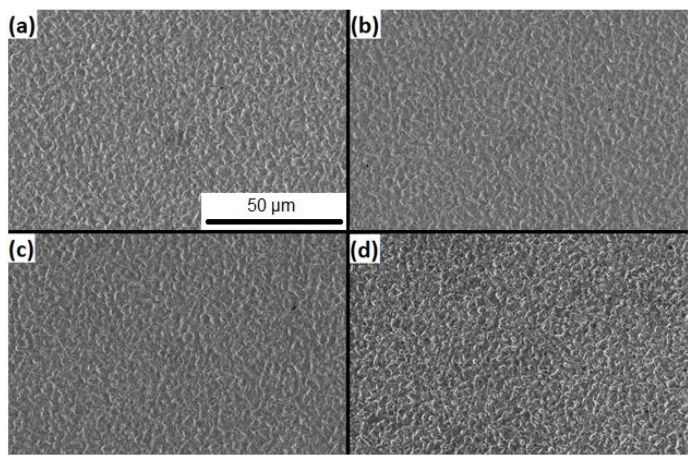
Figure 4.
Representative SEM images of Control #1 (control sample, i.e., without the NiO sublayer) (a) during the week of its preparation and (b) one, (c) four, (d) and eight months thereafter.
Figure 4.
Representative SEM images of Control #1 (control sample, i.e., without the NiO sublayer) (a) during the week of its preparation and (b) one, (c) four, (d) and eight months thereafter.

Figure 5.
Representative SEM images of Sample #1 (with NiO sublayer) (a) during the week of its preparation and (b) one, (c) four, (d) and eight months thereafter.
Figure 5.
Representative SEM images of Sample #1 (with NiO sublayer) (a) during the week of its preparation and (b) one, (c) four, (d) and eight months thereafter.


Table 1.
EDS values for exposed nickel oxide film (glass slide with sputtered copper substrate).
| Element | Percentage (Atomic) |
|---|---|
| Carbon | 14% |
| Oxygen | 36% |
| Silicon | 2% |
| Nickel | 3% |
| Copper | 46% |
Table 2.
EDS values for nickel oxide film following tin coating.
| Element | Percentage (Atomic) |
|---|---|
| Carbon | 1% |
| Oxygen | 6% |
| Nickel | 6% |
| Copper | 30% |
| Tin | 57% |
Table 3.
Summary of whisker counts and densities (mm−2) over time.
| C1 | C2 | S1 | S2 | |||||
|---|---|---|---|---|---|---|---|---|
| Count | Density | Count | Density | Count | Density | Count | Density | |
| Initial | 0 | 0 | 0 | 0 | 0 | 0 | 0 | 0 |
| 2 Weeks | 24 | 50.42 | 24 | 50.42 | 0 | 0.00 | 0 | 0 |
| 4 Weeks | 32 | 67.23 | 24 | 50.42 | 0 | 0.00 | 0 | 0 |
| 8 Weeks | 54 | 113.45 | 69 | 144.96 | 0 | 2.10 | 0 | 0 |
| 12 Weeks | 90 | 189.08 | 105 | 220.59 | 1 | 0.00 | 0 | 0 |
| 16 Weeks | 84 | 176.47 | 105 | 220.59 | 0 | 0.00 | 0 | 0 |
| 20 Weeks | 118 | 247.90 | 141 | 296.22 | 0 | 0.00 | 0 | 0 |
| 24 Weeks | 163 | 342.44 | 147 | 308.82 | 0 | 0.00 | 0 | 0 |
| 28 Weeks | 203 | 426.47 | 187 | 392.86 | 0 | 0.00 | 0 | 0 |
| 32 Weeks | 169 | 355.04 | 188 | 394.96 | 0 | 0.00 | 0 | 0 |
Publisher’s Note: MDPI stays neutral with regard to jurisdictional claims in published maps and institutional affiliations. |
© 2022 by the authors. Licensee MDPI, Basel, Switzerland. This article is an open access article distributed under the terms and conditions of the Creative Commons Attribution (CC BY) license (https://creativecommons.org/licenses/by/4.0/).
Share and Cite
MDPI and ACS Style
Buchanan, J.D.; Borra, V.; Islam, M.M.; Georgiev, D.G.; Itapu, S. Tin Whisker Growth Suppression Using NiO Sublayers Fabricated by Dip Coating. Condens. Matter 2022, 7, 7. https://0-doi-org.brum.beds.ac.uk/10.3390/condmat7010007
AMA Style
Buchanan JD, Borra V, Islam MM, Georgiev DG, Itapu S. Tin Whisker Growth Suppression Using NiO Sublayers Fabricated by Dip Coating. Condensed Matter. 2022; 7(1):7. https://0-doi-org.brum.beds.ac.uk/10.3390/condmat7010007
Chicago/Turabian StyleBuchanan, Jacob D., Vamsi Borra, Md Maidul Islam, Daniel G. Georgiev, and Srikanth Itapu. 2022. "Tin Whisker Growth Suppression Using NiO Sublayers Fabricated by Dip Coating" Condensed Matter 7, no. 1: 7. https://0-doi-org.brum.beds.ac.uk/10.3390/condmat7010007