UWB-MMIC Matrix Distributed Low Noise Amplifier †


Faculty of Sciences, Abdelmalek Essaâdi University, BP.2121 M’Hannech II, Tetuan 93030, Morocco
*
Author to whom correspondence should be addressed.
†
Presented at the 14th International Conference on Interdisciplinarity in Engineering—INTER-ENG 2020, Târgu Mureș, Romania, 8–9 October 2020.
Proceedings 2020, 63(1), 52; https://0-doi-org.brum.beds.ac.uk/10.3390/proceedings2020063052
Published: 25 December 2020
(This article belongs to the Proceedings of The 14th International Conference on Interdisciplinarity in Engineering—INTER-ENG 2020)
Abstract
:In this paper, a 3.1–11 GHz ultra-wideband low noise amplifier with low noise figure, high power gain S21, low reverse gain S12, and high linearity using the OMMIC ED02AH process, which employs a 0.18 μm Pseudomorphic High Electron Mobility Transistor is presented. This Low Noise Amplifier (LNA) was designed with the Advanced Design System simulator in distributed matrix architecture. For the low noise amplifier, four stages were used obtaining a good input/output matching. An average power gain S21 of 11.6 dB with a gain ripple of ±0.6 dB and excellent noise figure of 3.55 to 4.25 dB is obtained in required band with a power dissipation of 48 mW under a supply voltage of 2 V. The input compression point 1 dB and third-order input intercept point are −1.5 and 23 dBm respectively. The core layout size is 1.8 × 1.2 mm2.
Published: 25 December 2020
1. Introduction
With the growth of technological needs, especially in wireless communication, it was imperative for researchers to find and develop more structures compatible with modernity and which are aligned with global standards. In this context, we mention ultra-wideband (UWB) systems which were a source of interest for the most important industrial companies and institutes during the sixties of the previous century. As for recent years, these systems have several advantages, such as, high data rate transmission [1], high flexibility [2,3], low power spectra density [4], security [5], single chip architecture with small size, low cost and low power requirements [6]. Thus, systems performances are enhanced. According to Federal Communication Commission (FCC), UWB can be used in the field imaging systems (medical systems, Global Positioning Systems (GPS) and surveillance systems) or communications and measurement systems or vehicular Radar systems, allocating them a frequency domain of 3.1 to 10.6 GHz [7]. A critical component of UWB system is the Low Noise Amplifier, which aims to reduce the noise figure with large gain, low power consumption and stability necessary for eliminating self-oscillation [8].
The first distributed amplifier was studied in 1948 from pentode tubes [9]. The originality of principle lies in the fact that we got to take this advantage by the active elements in parallel while avoiding the disadvantages of reducing the input and output impedances. In distributed amplifiers, the active elements are placed between two propagation lines which carry out both an addition of the currents and adaptation to the source and to the load.
Today, distributed amplifiers have become good candidates for providing flat gain in a sufficiently wide band [10]. Monolithic microwave integrated circuit or MMIC technology seems a priori, the best suited to achieve this objective.
This paper is organized as follows. In Section 2, the characteristics of the ED02AH transistor device and the MMIC process will be presented. Section 3 gives a description of the proposed circuit and design considerations. Section 4 will discuss the results of a post-implementation simulation of proposed design techniques and compare them with those recently performed. The conclusion of this work will be presented in Section 5.
2. Device Characteristics and MMIC Process
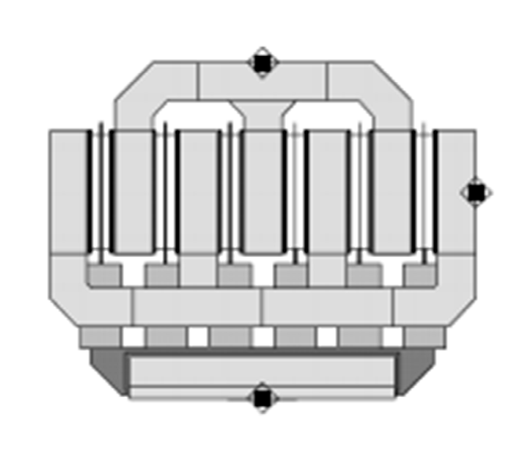
OMMIC ED02 commercial foundry provides several models for pseudomorphic High Electron Mobility transistors (pHEMTs) in the ED02AH technology. This uses six gate segments of 15 μm width each (6 × 15 μm ED02AH) as shown in Figure 1. Small signal linear models are given by scattering parameters versus bias points of a transistor. Nonlinear models include noises sources usually developed by manufacturers (Kacprzak and Materka model [11], Triquint foundry model [12], etc.).
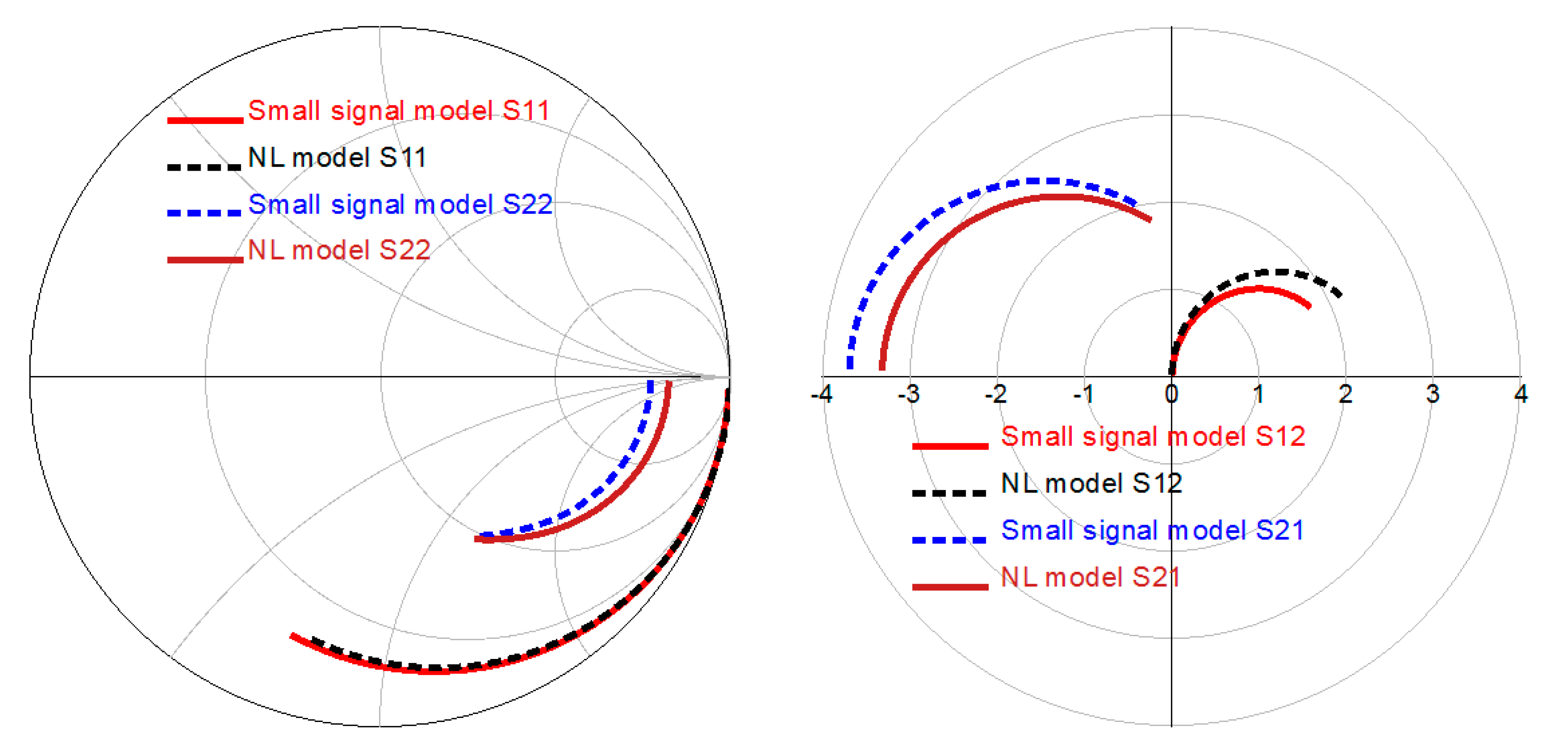
The typical results of the data comparison between the non linear and small signal model are shown in Figure 2 for the bias point ID = 16 mA and VDS = 2 V.
The error of the input and output reflection coefficients (S11 and S22) of the two models is weak compared to the direct and inverse gain parameters (S21 and S12) which can be as high as 30% when the frequency becomes larger. These Monolithic Microwave Integrated Circuit (MMIC) chips are fabricated with 0.18 μm pseudomorphic GaAs based HEMT technology, carried out by commercially available foundry. Table 1 summarizes the different characteristics of transistor ED02AH.
3. Circuit Description
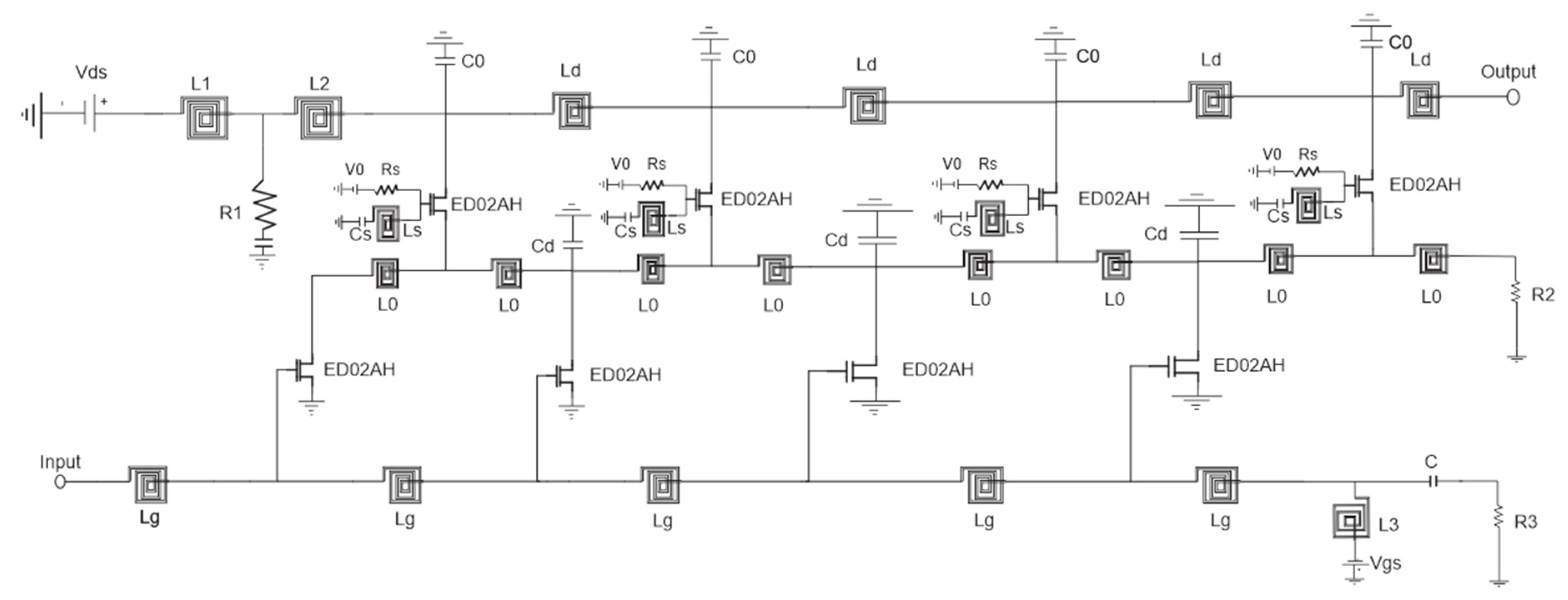
Figure 3 shows Ultra-Wideband Low Noise Amplifier (LNA) using MMIC technology. This LNA was designed in distributed matrix architecture. The noise resistor of transistor ED02AH depends on several parameters, which can be reduced using several short fingers (6 × 15 μm) or by increasing the number of stages. The amplifier that meets these criteria consists of six cells.
This Matrix architecture presents a very important gain for an ultra-wide frequency band. The resistive stability of the amplifier at high frequencies increases the value of the output conductance of the structure and at the same time degrades the gain of the amplifier [13]. Adjusting the reactive stability is an appropriate solution achieved by the means of the LsCs components of the gate of the transistor. A parallel resistor Rs is put in place to ensure the polarization of the circuit. The polarizations are fed via drain and gate lines. Inductances L1 and L3 must be dimensioned in order to have high impedance with respect to the Radio-Frequency RF signals. The module of the impedances ZLd and ZLg of these inductances is written as:
In order to ensure good RF signal transmission, the ZLd and ZLg impedance module must be greater than the characteristic impedance of the 50 Ω drain and gate lines at the minimum operating frequency. The Capacitors C0 and Cd are optimized to ensure a good adaptation in the frequency range studied. The values of different LNA parameters are shown in Table 2:
4. Results and Discussion
The proposed wideband LNA was simulated with a 0.18 μm GaAs-pHEMT ED02AH transistor. The performances of gain, noise, input/output matching, linearity, and power consumption are specified in order to regulate the values of the circuit components.
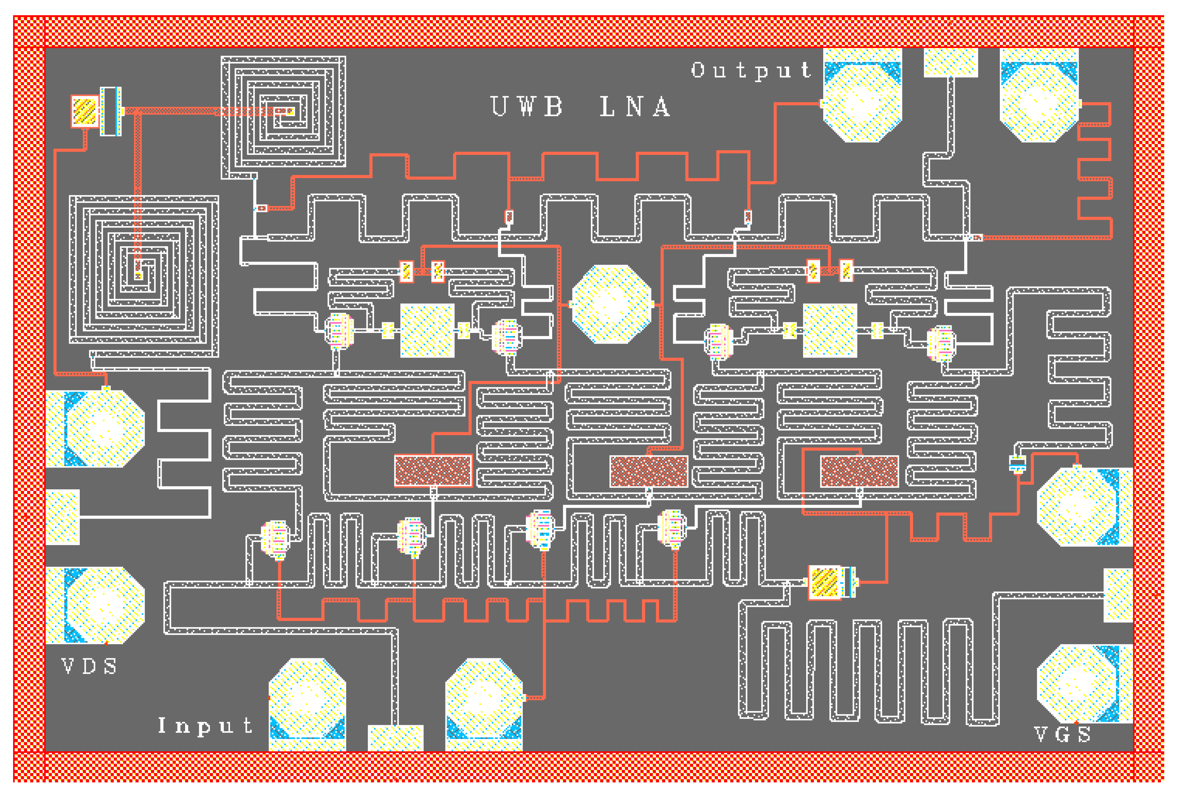
The final MMIC layout of the proposed wideband LNA is shown in Figure 4. The LNA is compact with the dimensions of 1.8 × 1.2 mm2.
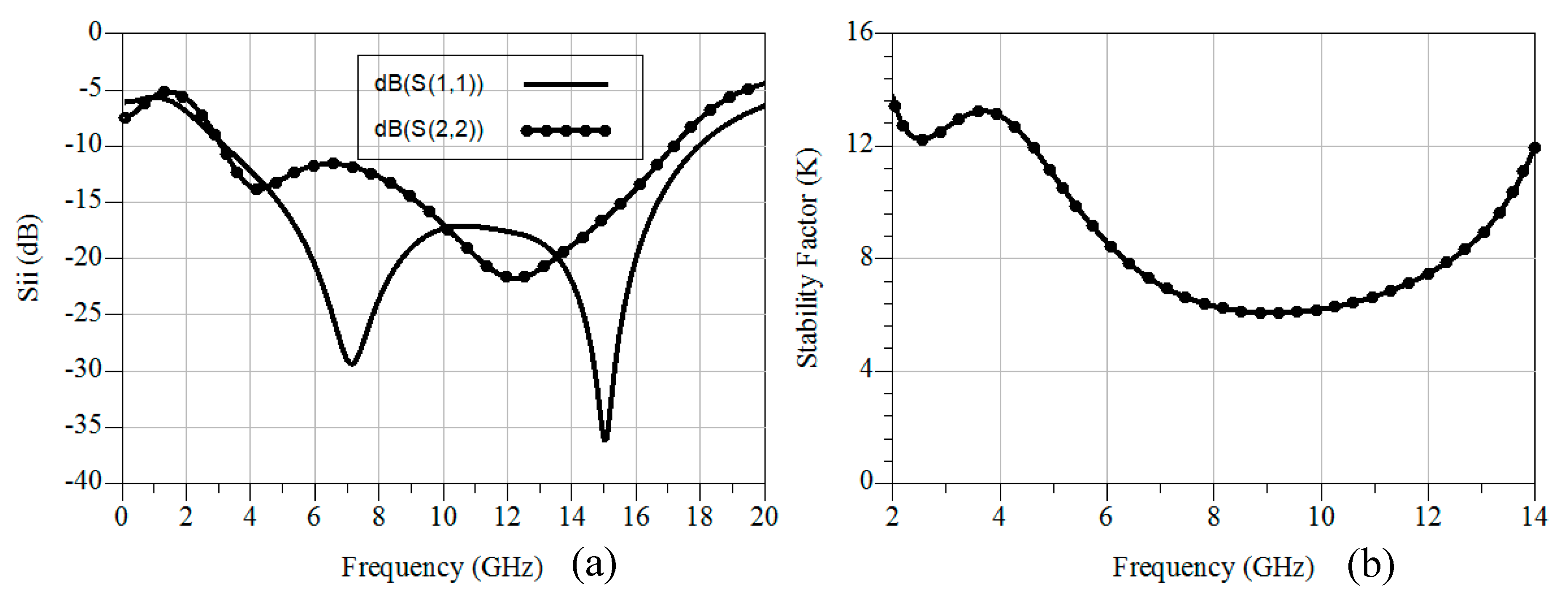
The simulated input and output reflections of LNA are shown in Figure 5a. Input and output reflections are less than −10 dB at all frequencies. The stability of LNA can be verified using Rollet’s K factor defined as in expression (3):
where, .
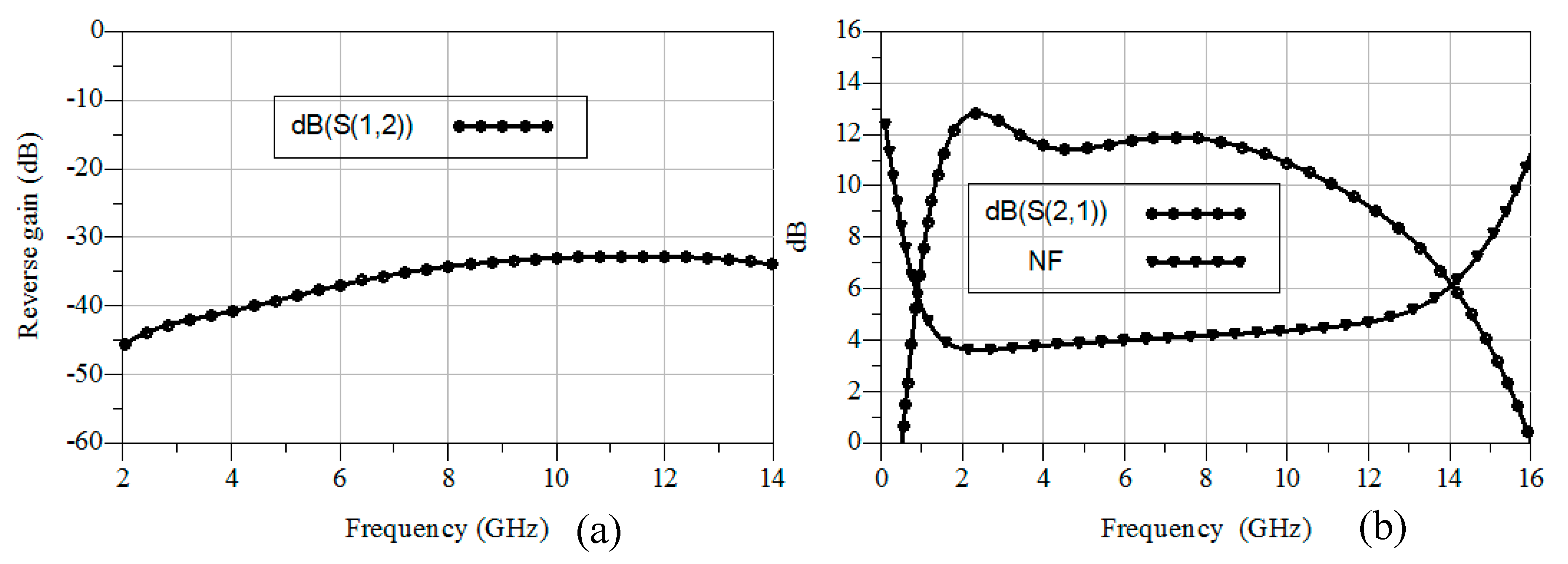
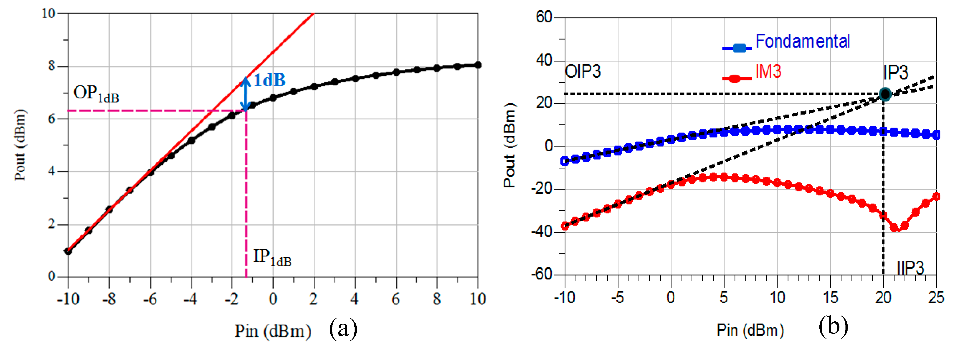
For unconditional stability, the condition K > 1 and ∆ < 1 must be satisfied. Figure 5b shows the value of K of LNA, which proves the unconditional stability over the entire band. It can be seen from Figure 6a that reverse gain S12 is less than −33 dB. Figure 6b proves an excellent noise figure (NF) as low as 3.65–4.35 dB in the required band with flat power gain of {11–12.2} dB and a consumption of 48 mW under a supply voltage of 2 V. Linearity is another important LNA parameter. The 1 dB compression point and third-order intercept point (IP3) represent the non linear operating domain of RF circuits that helps in proving a circuit’s linearity and dynamic range. By generating a two-tone input signal with a separation frequency of 10 MHz, the intermodulation point IM is the point of intersection between the fundamental spectrum and the third-order intercept point IP3. The output IP3 was calculated with Equation (4).
Figure 7 shows that the compression point occurs for −1.5 dBm and the third-order input interception point (IIP3) is about 20 dBm for input RF power.
The performance analysis with comparison of current works with recent literature was shown in Table 3.
5. Conclusions
An Ultra-wideband LNA using MMIC technology with 0.18 μm- pHEMT ED02AH transistor was designed in distributed matrix architecture. The input/output matching conditions were satisfied by parallel capacitance. Stability was enhanced by an LC resonant circuit used in series with the transistor gate. From 3.1 to 11 GHz and with 2 V supply voltage, the amplifier’s noise figure is 3.9 ± 0.35 dB. The average power gain is 11.9 dB. The power consumption is 48 mW. Due to wideband and high linearity, the proposed LNA is a suitable choice for multi-standard and UWB applications.
References
- Intel White Paper. Ultra-Wideband (UWB) Technology: Enabling High-Speed Wireless Personal Area Networks; Intel: Santa Clara, CA, USA, 2004. [Google Scholar]
- Chong, C.C.; Yong, S.K.; Kim, Y.-H.; Kim, J.-H.; Lee, S.-S. Samsung Electronics (SAIT) CFP Presentation for IEEE 802.15.4a Alternative PHY: UWB Direct Chaotic Communication System. In Proceedings of the IEEE 802.15-05- 0030-02-004a, Monterey, CA, USA, 26 January 2005. [Google Scholar]
- Chong, C.-C.; Yong, S.K. On the performance of non-coherent and differential-coherent UWB-DCC system. In Proceedings of the IEEE Wireless Commun. and Networking Conf., Las Vegas, NV, USA, 3–6 April 2006. [Google Scholar]
- Giuliano, R.; Mazzenga, F. On the coexistence of power-controlled ultra wide-band systems with UMTS, GPS, DCS1800, and fixed wireless systems. IEEE Trans. Veh. Technol. 2005, 54, 62–81. [Google Scholar] [CrossRef]
- McKinstry, D.R.; Buehrer, R.M. Issues in the performance and covertness of UWB communications systems. In Proceedings of the 45th Midwest Symposium on Circuits and Systems, Tulsa, OK, USA, 5–7 August 2002; Volume 3, pp. 601–604. [Google Scholar]
- Namgoong, W. A channelized digital ultrawideband receiver. IEEE Trans. Wirel. Commun. 2003, 2, 502–510. [Google Scholar] [CrossRef]
- Federal Communications Commission. Revision of Part 15 of the Commission’s Rules Regarding Ultra-Wide Band Transmission Systems; First Report and Order (ET Docket 98–153); Federal Communications Commission: Washington, DC, USA, 2002. [Google Scholar]
- Lei, Y.; Viktor, K.; S’ebastien, D.; Vitaliy, Z.; Tom, K.J.; Chenhui, J. GaAs Wideband Low Noise Amplifier Design for Breast Cancer Detection System 978-1-4244-2802-1/09/2009 IEEE. IEEE Micro 2010, 8, 357–360. [Google Scholar]
- Percival, W.S. Thermionic Valve Circuits. British Patent 460562, 25 January 1937. [Google Scholar]
- Moustapha, E.B.; Hanae, E.; Naima, A.T.; Elhamadi, T. 2.3–21 GHz broadband and high linearity distributed low noise amplifier. Integration 2020, 76, 61–68. [Google Scholar] [CrossRef]
- Materka, A.; Kacprzak, T. Computer calculation of large-signal GaAs FET amplifier characteristics. IEEE Trans. MTT 1985, MTT-33, 129–135. [Google Scholar] [CrossRef]
- Smith, D. TOM-2: An Improved Model for GaAs MESFET; Internal Memorandum; Triquint Semiconductor Inc.: Hillsboro, OR, USA, 1995. [Google Scholar]
- Ming, D.T.; Kuo, L.D.; Huei, W.; Chun, H.C.; Chih, S.C.; Chern, J.G.J. A miniature 25-GHz 9-dB CMOS cascaded single-stage distributed amplifier. IEEE Microw. Wirel. Compon. Lett. 2004, 14, 554–556. [Google Scholar] [CrossRef]
- Chen, C.C.; Wang, Y.C. 3.1–10.6 GHz ultra-wideband LNA design usingdual-resonant broadband matching technique. Int. J. Electron. Commun. 2013, 67, 500–503. [Google Scholar] [CrossRef]
- Rastegar, H.; Ryu, J.Y. A broadband Low Noise Amplifier with built-in linearizer in 0.13-µm CMOS process. Microelectron. J. 2015, 46, 698–705. [Google Scholar] [CrossRef]
- Saberkari, A.; Kazemi, S.; Shirmohammadli, V.; Yagoub, M.C.E. gm-boosted flat gain UWB low noise amplifier with active inductor-based input matching network. Integr. VLSI J. 2016, 52, 323–333. [Google Scholar] [CrossRef]
Figure 1.
ED02AH 6 × 15 μm layout.

Figure 2.
Scattering parameters comparison of linear and NL ED02AH models transistor in frequency range of 0.5 to 30 GHz (Vgs = −0.3 V and Vds= 2 V).
Figure 2.
Scattering parameters comparison of linear and NL ED02AH models transistor in frequency range of 0.5 to 30 GHz (Vgs = −0.3 V and Vds= 2 V).

Figure 3.
Schematic of the Low Noise Amplifier (LNA).

Figure 4.
Photograph of the Monolithic Microwave Integrated Circuit (MMIC) Low Noise Amplifier (1.8 × 1.2 mm2).
Figure 4.
Photograph of the Monolithic Microwave Integrated Circuit (MMIC) Low Noise Amplifier (1.8 × 1.2 mm2).

Figure 5.
Simulated results of: (a) input/output reflection coefficients and, (b) LNA Stability.

Figure 6.
Simulated results of: (a) isolation, and (b) Simulated results of power gain and noise figure (NF).
Figure 6.
Simulated results of: (a) isolation, and (b) Simulated results of power gain and noise figure (NF).

Figure 7.
Simulated results of: (a) compression point 1 dB, and (b) Interception point (IP3).


Table 1.
The physical characteristics of transistor ED02AH.
| Process | Tech | Gate Length | Thickness | Ft | Fmax | Gm |
|---|---|---|---|---|---|---|
| ED02AH pHEMT | GaAs | 0.18 μm | 100 μm | 60 GHz | 110 GHz | 450 ms/mm |
| Vbgd (V) | Vdsmax (V) | Idss (mA/mm) | Idss max(mA/mm) | NF (dB) | Power Density | |
| 8 | 7 | 250(on)/140(off) | 400(on)/180(off) | 0.8(18GHz) | 330 (mW/mm) |
Table 2.
Optimization result of different LNA parameters.
| L1 (nH) | L2 (nH) | L3 (nH) | Ld (nH) | Lg (nH) | Ls (nH) | Lo (nH) |
| 4.212 | 2.088 | 2.67 | 0.3948 | 0.488 | 0.3 | 0.7835 |
| R1 (Ω) | R2 (Ω) | R3 (Ω) | Rs (Ω) | Cd (pF) | Cs (pF) | Co (fF) |
| 57 | 100 | 49 | 100 | 0.3 | 0.247 | 10 |
Table 3.
UWB LNA performance comparison.
| [14] | [15] | [16] | This Work | |
|---|---|---|---|---|
| Technology(μm) | 0.18-CMOS | 0.13-CMOS | 0.18-CMOS | 0.2-pHEMT |
| Supply voltage (V) | N/A | N/A | N/A | 2 |
| Bandwidth (GHz) | 3.1–10.6 | 3.1–10.6 | 3.1–10.6 | 3.1–11 |
| Pdc(mW) | N/A | 17.92 | 13.6 | 48 |
| S11 (dB) | <−8.8 | <−8 | <−9.5 | <−10 |
| S22 (dB) | N/A | N/A | N/A | <−10 |
| S21 (dB) | 11 max | 10.24 max | 12.1±0.7 | 11.6 ± 0.6 |
| NF (dB) | 3.95 ± 0.75 | 0.9–4.1 | 4.56–4.7 | 3.9 ± 0.35 |
| S12 (dB) | N/A | −31 | N/A | −33 |
| P1dB (dBm) | N/A | N/A | N/A | −1.5 |
| IIP3 (dBm) | 6 | 6.8 | −12.5 | 20 |
| Die area (mm2) | 0.7 × 0.8 | N/A | N/A | 1.8 × 1.2 |
Publisher’s Note: MDPI stays neutral with regard to jurisdictional claims in published maps and institutional affiliations. |
© 2020 by the authors. Licensee MDPI, Basel, Switzerland. This article is an open access article distributed under the terms and conditions of the Creative Commons Attribution (CC BY) license (http://creativecommons.org/licenses/by/4.0/).
Share and Cite
MDPI and ACS Style
Bakkali, M.E.; Elkhaldi, S.; Hamzi, I.; Marroun, A.; Touhami, N.A. UWB-MMIC Matrix Distributed Low Noise Amplifier. Proceedings 2020, 63, 52. https://0-doi-org.brum.beds.ac.uk/10.3390/proceedings2020063052
AMA Style
Bakkali ME, Elkhaldi S, Hamzi I, Marroun A, Touhami NA. UWB-MMIC Matrix Distributed Low Noise Amplifier. Proceedings. 2020; 63(1):52. https://0-doi-org.brum.beds.ac.uk/10.3390/proceedings2020063052
Chicago/Turabian StyleBakkali, Moustapha El, Said Elkhaldi, Intissar Hamzi, Abdelhafid Marroun, and Naima Amar Touhami. 2020. "UWB-MMIC Matrix Distributed Low Noise Amplifier" Proceedings 63, no. 1: 52. https://0-doi-org.brum.beds.ac.uk/10.3390/proceedings2020063052