Micro Flowers of SrS/Bi2S3 Nanocomposite and Its Field Emission Properties

Abstract
:
1. Introduction
2. Materials and Methods
2.1. Material
2.2. Synthesis of SrS/Bi2S3
2.3. Sample Characterizations
2.4. Field Emission
3. Results and Discussions
3.1. Structural Study
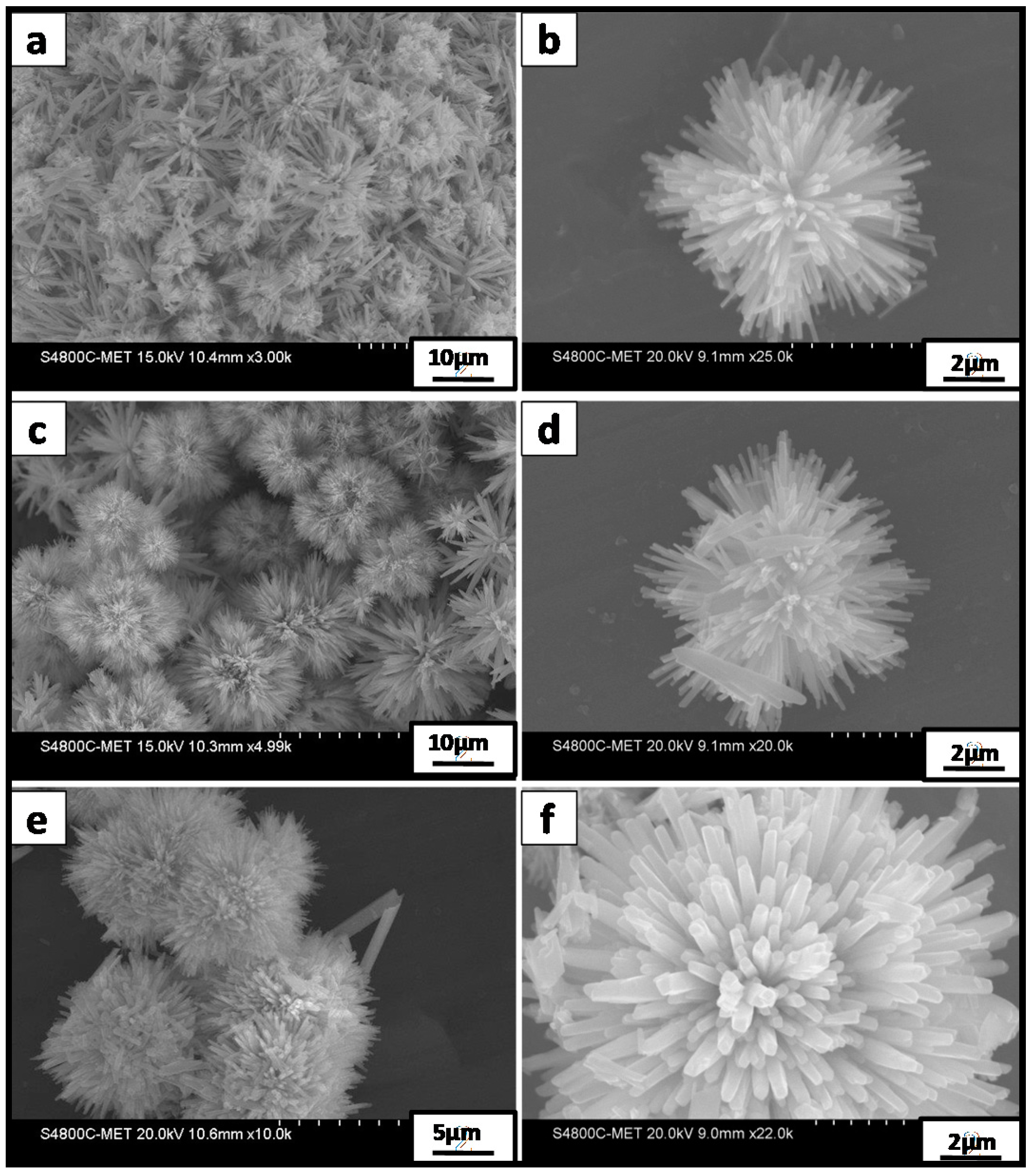
3.2. FESEM Study
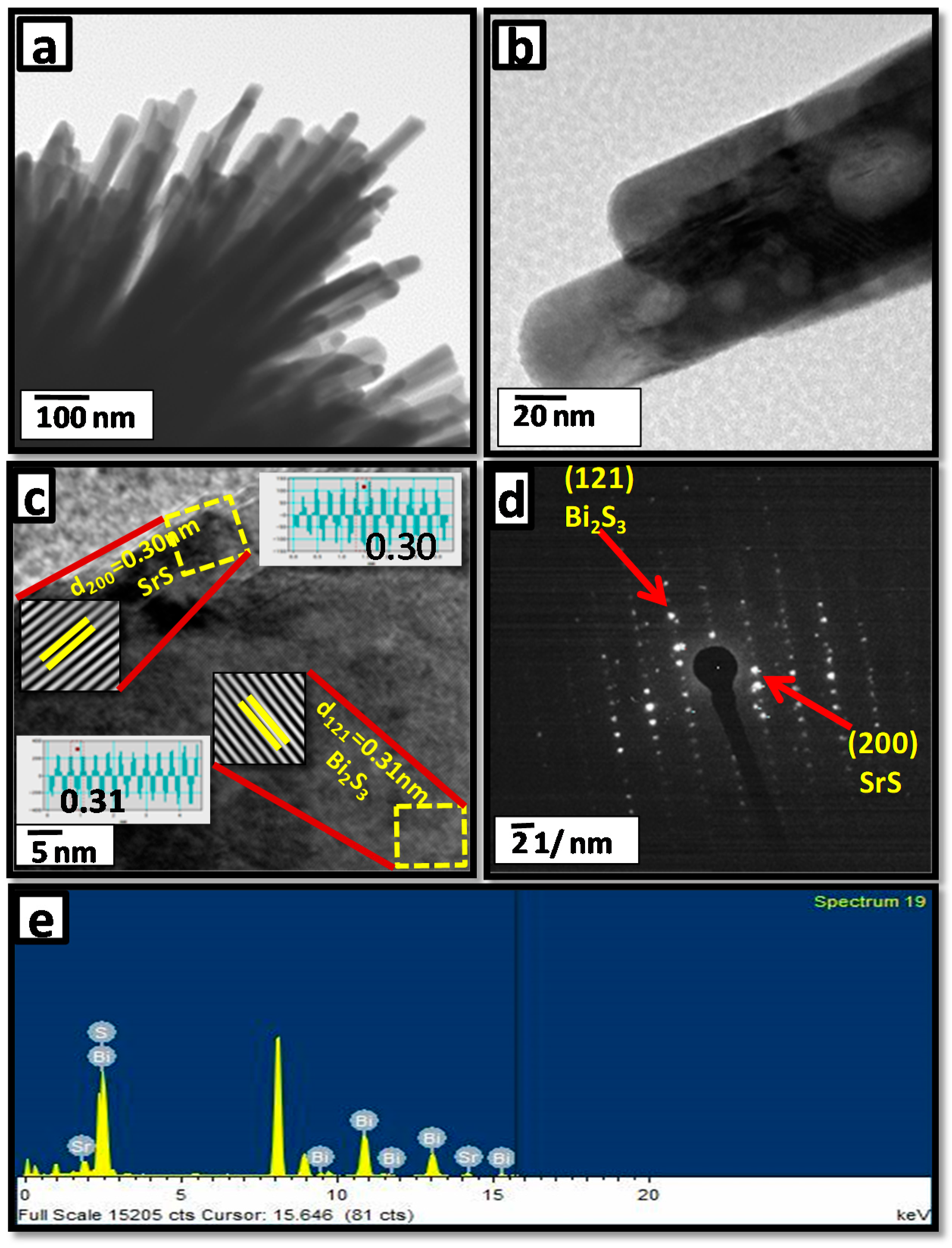
3.3. HR-TEM Study
3.4. Optical and Electronic Studies
3.5. PL Study
3.6. Raman Study
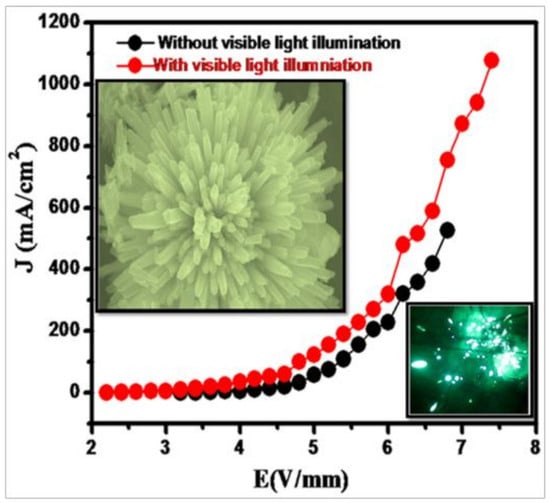
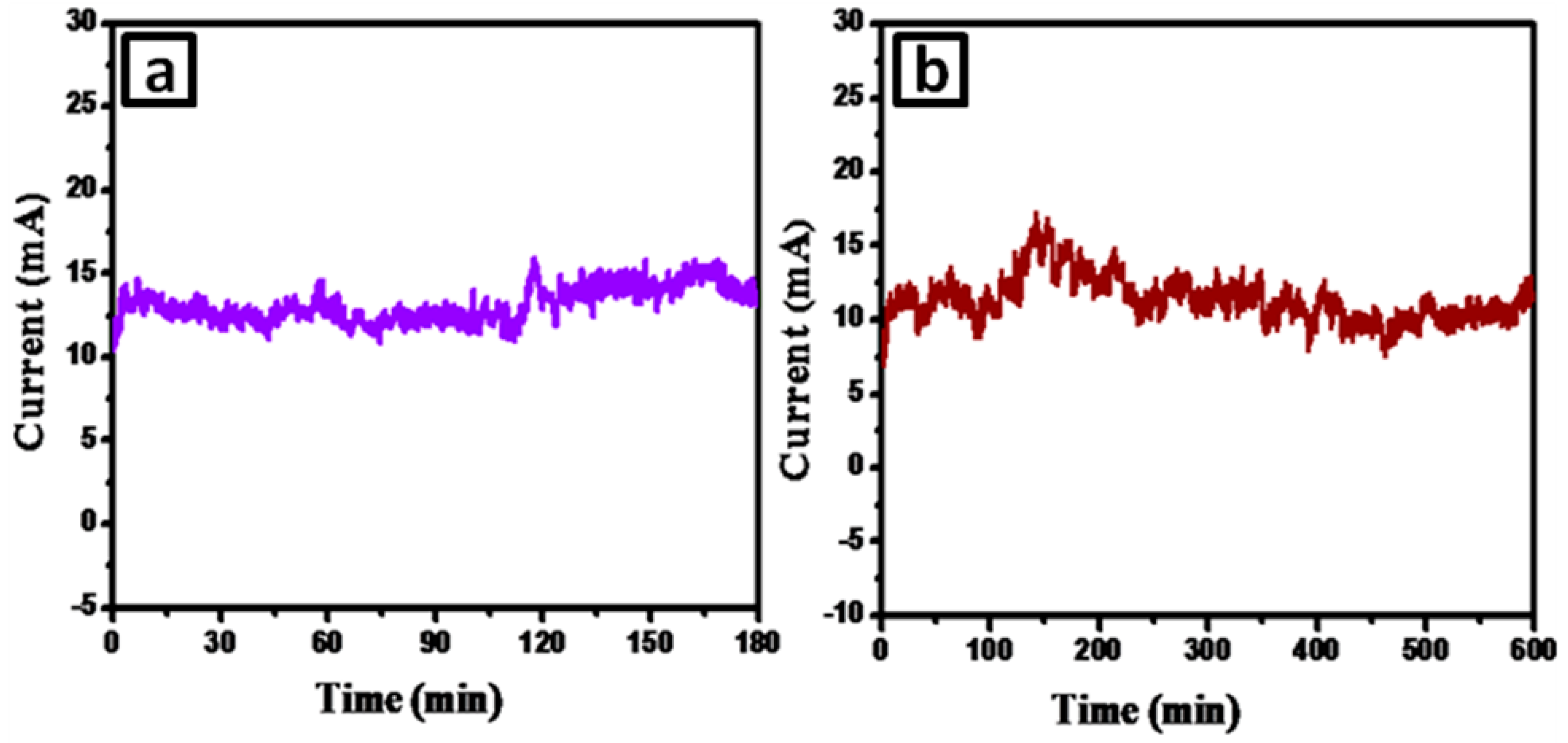
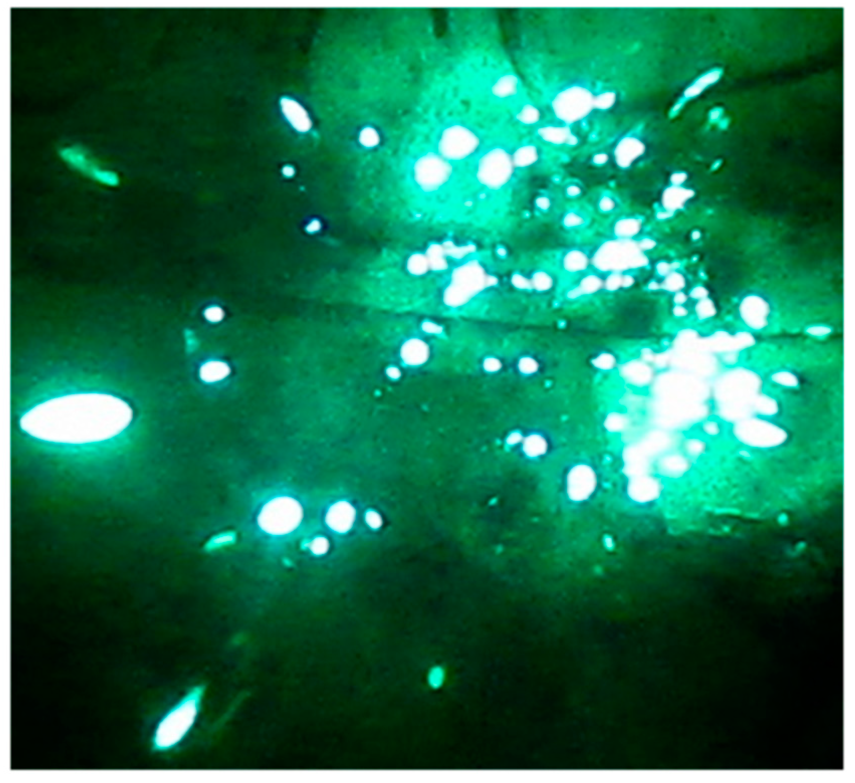
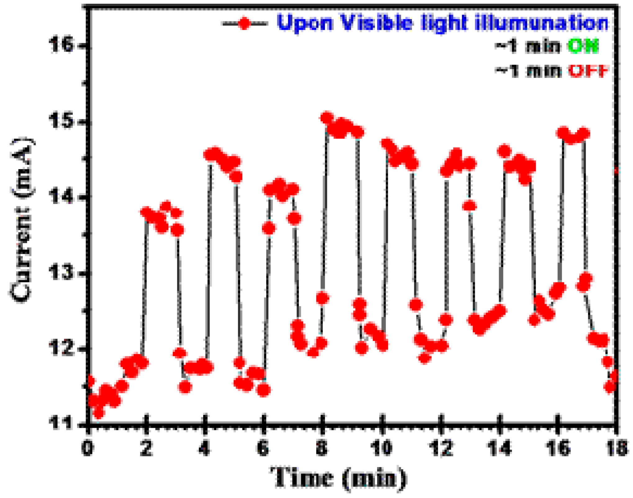
4. Field Emission Study (FE)
5. Conclusions
Supplementary Materials
Author Contributions
Funding
Acknowledgments
Conflicts of Interest
References
- Yu, X.; Cao, C. Photoresponse and Field-Emission Properties of Bismuth Sulfide Nanoflowers. Cryst. Growth Des. 2008, 8, 3951. [Google Scholar] [CrossRef]
- Zhai, T.L.; Ma, L.Y.; Liao, M.; Wang, X.; Fang, X.; Yao, J.; Bando, Y.; Golberg, D. One-dimensional inorganic nanostructures: Synthesis, field-emission and photodetection. Chem. Soc. Rev. 2011, 40, 2986. [Google Scholar] [CrossRef] [PubMed]
- Panmand, R.P.; Sethi, Y.A.; Deokar, R.S.; Late, D.J.; Gholap, H.M.; Baeg, J.; Kale, B.B. In situ fabrication of highly crystalline CdS decorated Bi2S3 nanowires (nano-heterostructure) for visible light photocatalyst application. RSC Adv. 2016, 6, 23508–23517. [Google Scholar] [CrossRef]
- Yu, Y.; Jin, C.H.; Wang, R.H.; Chen, Q.; Peng, L.-M. High-Quality Ultralong Bi2S3 Nanowires: Structure, Growth, and Properties. J. Phys. Chem. B 2005, 109, 18772–18776. [Google Scholar] [CrossRef] [PubMed]
- Warule, S.S.; Kashid, R.V.; Shinde, D.R.; Chaudhari, N.S.; Kale, B.B.; More, M.A. Architectured Bi2S3 nanoflowers: Photoenhanced field emission study. J. Nanopart Res. 2012, 14, 889. [Google Scholar] [CrossRef]
- Ibanez, M.; Guardia, P.; Shavel, A.; Cadavid, D.; Arbiol, J.; Morante, J.; Cabot, A. Growth Kinetics of Asymmetric Bi2S3 Nanocrystals: Size Distribution Focusing in Nanorods. Phys. Chem. C 2011, 115, 7947. [Google Scholar] [CrossRef]
- Ramgir, N.S.; Late, D.J.; Bhise, A.B.; Mulla, I.S.; More, M.A.; Joag, D.S.; Pillai, V.K. Field emission studies of novel ZnO nanostructures in high and low field regions. Nanotechnology 2006, 17, 2730. [Google Scholar] [CrossRef]
- Khan, Z.; Barpuzary, D.; Baswant, O.; Sutradhar, S.; Qureshi, M. Directed growth of 1D cadmium sulfide by chemically anchored Al2O3 and ZnO (nanoparticles). Mater. Lett. 2011, 65, 1168. [Google Scholar] [CrossRef]
- Li, F.B.; Li, X.Z. The enhancement of photodegradation efficiency using Pt-TiO2 catalyst. Chemosphere 2002, 48, 1103. [Google Scholar] [CrossRef] [Green Version]
- Zhang, J.; Hu, Y.; Matsuoka, M.; Yamashita, H.; Minagawa, M.; Hidaka, H. Relationship between the Local Structures of Titanium Oxide Photocatalysts and Their Reactivities in the Decomposition of NO. J. Phys. Chem. B 2001, 105, 8395. [Google Scholar] [CrossRef]
- Cong, Y.; Zhang, J.; Chen, F.; Anpo, M.; He, D. Preparation, Photocatalytic Activity, and Mechanism of Nano-TiO2 Co-Doped with Nitrogen and Iron (III). J. Phys. Chem. C 2007, 111, 10618. [Google Scholar] [CrossRef]
- Niasaria, M.S.; Ghanbaria, D.; Davara, F. Synthesis of different morphologies of bismuth sulfide nanostructures via hydrothermal process in the presence of thioglycolic acid. J. Alloys Compd. 2009, 488, 442. [Google Scholar] [CrossRef]
- Wang, Y.; Chen, J.; Jiang, L.; Sun, K.; Liu, F.; Lai, Y. Photoelectrochemical properties of Bi2S3 thin films deposited by successive ionic layer adsorption and reaction (SILAR) method. J. Alloys Compd. 2016. [Google Scholar]
- Campbell, I.H.; Fauchet, P.M. The effects of microcrystal size and shape on the one phonon Raman spectra of crystalline semiconductors. Sol. State Commun. 1986, 58, 739. [Google Scholar] [CrossRef]
- Liu, Z.; Huang, W.; Zhang, Y.; Tong, Y. Facile hydrothermal synthesis of Bi2S3 spheres and CuS/Bi2S3 composites nanostructures with enhanced visible-light photocatalytic performances. CrystEngComm 2014, 12, 8261. [Google Scholar] [CrossRef]
- Kar, S.; Chaudhuri, S.C.J. Shape Selective Growth of CdS One-Dimensional Nanostructures by a Thermal Evaporation Process. J. Phys. Chem. B 2006, 110, 4542. [Google Scholar] [CrossRef]
- Warule, S.S.; Chaudhari, N.S.; Kale, B.B.; Pandiraj, S.; Khare, R.T.; More, M.A. Controlled synthesis of aligned Bi2S3 nanowires, sharp apex nanowires and nanobelts with its morphology dependent field emission investigations. CrystEngComm 2013, 15, 890. [Google Scholar] [CrossRef]
- Fowler, R.H.; Nordheim, L.W.; Proc, R. Electron emission in intense electric fields. London. Ser. A 1928, 119, 173. [Google Scholar] [CrossRef]
- Palnitkar, U.A.; Kashid, R.V.; More, M.A.; Joag, D.S.; Panchakarla, L.S.; Rao, C.N.R. Remarkably low turn-on field emission in undoped, nitrogen-doped, and boron-doped graphene. Appl. Phys. Lett. 2010, 97, 063102. [Google Scholar] [CrossRef]
- Chavan, P.G.; Badadhe, S.S.; Mulla, I.S.; More, M.A.; Joag, D.S. Synthesis of single crystalline CdS nanocombs and their application in photo-sensitive field emission switches. Nanoscale 2011, 3, 1078–1083. [Google Scholar] [CrossRef]
- Bankar, P.K.; Pawar, M.S.; Pawbake, A.S.; Warule, S.S.; Late, D.J.; More, M.A. Spatially branched CdS–Bi2S3 heteroarchitecture: Single step hydrothermal synthesis approach with enhanced field emission performance and highly responsive broadband photodetection. RSC Adv. 2016, 6, 95092–95100. [Google Scholar] [CrossRef]
- Zhirnov, V.V.; Givargizov, E.I.; Plekhanov, P.S. Field emission from silicon spikes with diamond coatings. J. Vac. Sci. Technol. 1995, 13, 418–421. [Google Scholar] [CrossRef]
- Warule, S.S.; Chaudhari, N.S.; Kale, B.B.; Patil, K.R.; Koinkar, P.M.; More, M.A.; Murakami, R.-I. Organization of cubic CeO2 nanoparticles on the edges of self assembled tapered ZnO nanorods via a template free one-pot synthesis: Significant cathodoluminescence and field emission properties. J. Mater. Chem. 2012, 22, 8887–8895. [Google Scholar] [CrossRef]


| Specimen | Turn-on Field For 1 μA/cm² V/μm Light Off/On | Threshold Field 10 μA/cm² V/μm Light Off/On | Maximum Current Density µA/cm2 Light Off/On |
|---|---|---|---|
| Bi2S3 pristine | 3.10 | 3.84 | 60.32 |
| S1 | ca. 6.9/ca. 2.50 | ca. 7.4/ca. 3.20 | ca. 254/ca. 173 |
| S2 | ca. 2.55/ca. 2.37 | ca. 3.07/ca. 2.68 | ca. 264/ca. 284.8 |
| S3 | ca. 2.50/ca. 2.10 | ca. 3.00/ca. 2.80 | ca. 527/ca. 1078 |
© 2019 by the authors. Licensee MDPI, Basel, Switzerland. This article is an open access article distributed under the terms and conditions of the Creative Commons Attribution (CC BY) license (http://creativecommons.org/licenses/by/4.0/).
Share and Cite
Gunjal, A.R.; Chothe, U.P.; Sethi, Y.A.; Panmand, R.P.; Ambekar, J.D.; Kulkarni, M.V.; More, M.A.; Kale, B.B. Micro Flowers of SrS/Bi2S3 Nanocomposite and Its Field Emission Properties. J. Compos. Sci. 2019, 3, 105. https://0-doi-org.brum.beds.ac.uk/10.3390/jcs3040105
Gunjal AR, Chothe UP, Sethi YA, Panmand RP, Ambekar JD, Kulkarni MV, More MA, Kale BB. Micro Flowers of SrS/Bi2S3 Nanocomposite and Its Field Emission Properties. Journal of Composites Science. 2019; 3(4):105. https://0-doi-org.brum.beds.ac.uk/10.3390/jcs3040105
Chicago/Turabian StyleGunjal, Aarti R., Ujjwala P. Chothe, Yogesh A. Sethi, Rajendra P. Panmand, Jalinder D. Ambekar, Milind V. Kulkarni, Mahendra A. More, and Bharat B. Kale. 2019. "Micro Flowers of SrS/Bi2S3 Nanocomposite and Its Field Emission Properties" Journal of Composites Science 3, no. 4: 105. https://0-doi-org.brum.beds.ac.uk/10.3390/jcs3040105