Design and Fabrication of Broad-Beam Microstrip Antenna Using Parasitic Patches and Cavity-Backed Slot Coupling


Department of Electrical and Computer Engineering, Faculty of Engineering, Mahasarakham University, Maha Sarakham 44150, Thailand
*
Author to whom correspondence should be addressed.
Appl. Syst. Innov. 2022, 5(2), 31; https://0-doi-org.brum.beds.ac.uk/10.3390/asi5020031
Submission received: 30 December 2021
/
Revised: 20 February 2022
/
Accepted: 22 February 2022
/
Published: 24 February 2022
Abstract
:The adjusting parasitic patch size technique for the broad-beam microstrip antenna array using the cavity-backed slot coupling is presented. The phase of each element of the microstrip array has been designed to emulate the reflection of waves on the surface of parabolic backscattering. In order to increase the efficiency of this array antenna, the back-slot cavity with an exciting probe will be employed for coupling the electromagnetic waves to the back of this array. The proper sizes and locations of patches and the optimized position of the cavity have been investigated by the Computer Science Technology (CST) Microwave Studio. The gain, the radiation pattern, the bandwidth, and the return loss are extensively analyzed. The fabricated antenna has the return loss of −22.39 dB, the bandwidth of 47 MHz (4.975–5.022 GHz), and the maximum directive gain of 5.6 dB at 5 GHz, and it can produce a wide beam width (half-power beam width around 130°). The antenna could be applied for wide applications in the wireless communications system. In particular, this realizing antenna covers the low earth orbit (LEO) satellite beam.
1. Introduction
The antenna technology for the space and geographical information system (GIS), especially the low earth orbit (LEO) satellite communication systems, has been extensively investigated. There are many applications using microstrip lines as the components of the communication devices [1,2,3]. Thanks to its high gain and narrow beam, the parabolic reflector antenna is most widely employed in satellite communications. However, the feed horns and their arms are mounted at the front of the reflector, giving rise to obstruction on the aperture, and this, at long last, results in its downgraded efficiency while the large curvature generally affects the aerodynamic motion of the satellite when launched into the orbit. In order to solve these problems, the novel types of the microstrip array antennas are specially designed [4,5,6,7]. Importantly, the dimensions and the planar shapes of the microstrip array have no limitation and less distortion, respectively. The parabolic reflector is applied for operation. Additionally, there are a number of advantages of the microstrip array i.e., its low cost, its small size, its light weight, and its easy installation.
In order to overcome the limitations of the time requirements for an earth station communicating with the LEO satellite moving at a very high speed with wide beam antennas, the shaped beam antenna is first developed, which is the earth coverage from the satellite antenna [8,9,10,11,12]. Recently, to satisfyingly meet the similar requirements, the shaped reflector antenna has been considerably favorable to many other types, but this antenna is not coverage of the earth from satellite antennas [13,14]. Yielding the similar results to the parabolic backscattering techniques, those of the microstrip reflectarray duplicated the same radiating aperture [15,16].
In this paper, an analytic design of the broad-beam microstrip antenna (MSA) array using the cavity-backed slot coupling is presented. The structure of this cavity-backed, [17,18,19] slot-coupled microstrip patch [20,21,22] is excited by a linear electric probe, which is mounted at the inner surface of the rectangular cavity [23]. In order to achieve the broad-beam antenna, the phase of each array element in the microstrip array antennas is specifically designed. This design emulates the function of curvature of the parabolic backscattering by modifying the parameters of the parasitic patch array around the radiation patches. These parameters are as follows: the patch sizes, the slot length, the slot width, the probe length, the cavity positions, and the gaps. Consequently, this proposed technique has been investigated and monitored by computer simulation technology software. Finally, the proposed antenna is fabricated and its performance is measured and then compared with that of the simulation. The proposed antenna has the potential to be applied to a LEO satellite for an earth coverage beam or used for other applications in a wireless communications system, particularly WLAN [24,25,26] and sub-6 GHz 5G communications [27,28,29].
2. Antenna Structure
Figure 1 shows the geometry modification of the 5 × 5 microstrip patch parasitic array using the cavity-backed slot. The proposed antenna is fabricated on a 100 mm × 100 mm double-sided FR4 epoxy where a dielectric constant (εr) and a substrate of thickness ‘d’ are 4.4 and 0.8 mm, respectively. In order to obtain the optimized return loss and the widest beam radiation pattern, the antenna parameters and the positions of each patch element have been successfully simulated by means of the CST Microwave Studio simulation [30]. As shown in Table 1, the dimensions of the broad-beam configuration have been designed for the operating frequency of 5.0 GHz. The 5 × 5 square patch lengths ‘lp’ are printed on the upper side of an FR4 substrate. The rectangular slot length ‘ls’ and width ‘ws’ are etched in the center of the antenna ground plane and then covered with the rectangular metallic cavity. The slot itself must not resonate over the operating frequency bands of the antenna due to the radiation from this slot interfering from the patches. The length of the exciting probe ‘lf’ is installed at the cavity center. The center of the slot and the radiating patch are considered the origin point (0,0). The dimensions of the rectangular cavity are designed of the dominant mode (TE101) with length ‘cx’, width ‘cy’, height ‘cz’, and the installing position ‘dy’, which is an important parameter to acquire the best return loss.
3. Simulated Results and Analysis
3.1. Effects of the Single Patch and the Patch Array
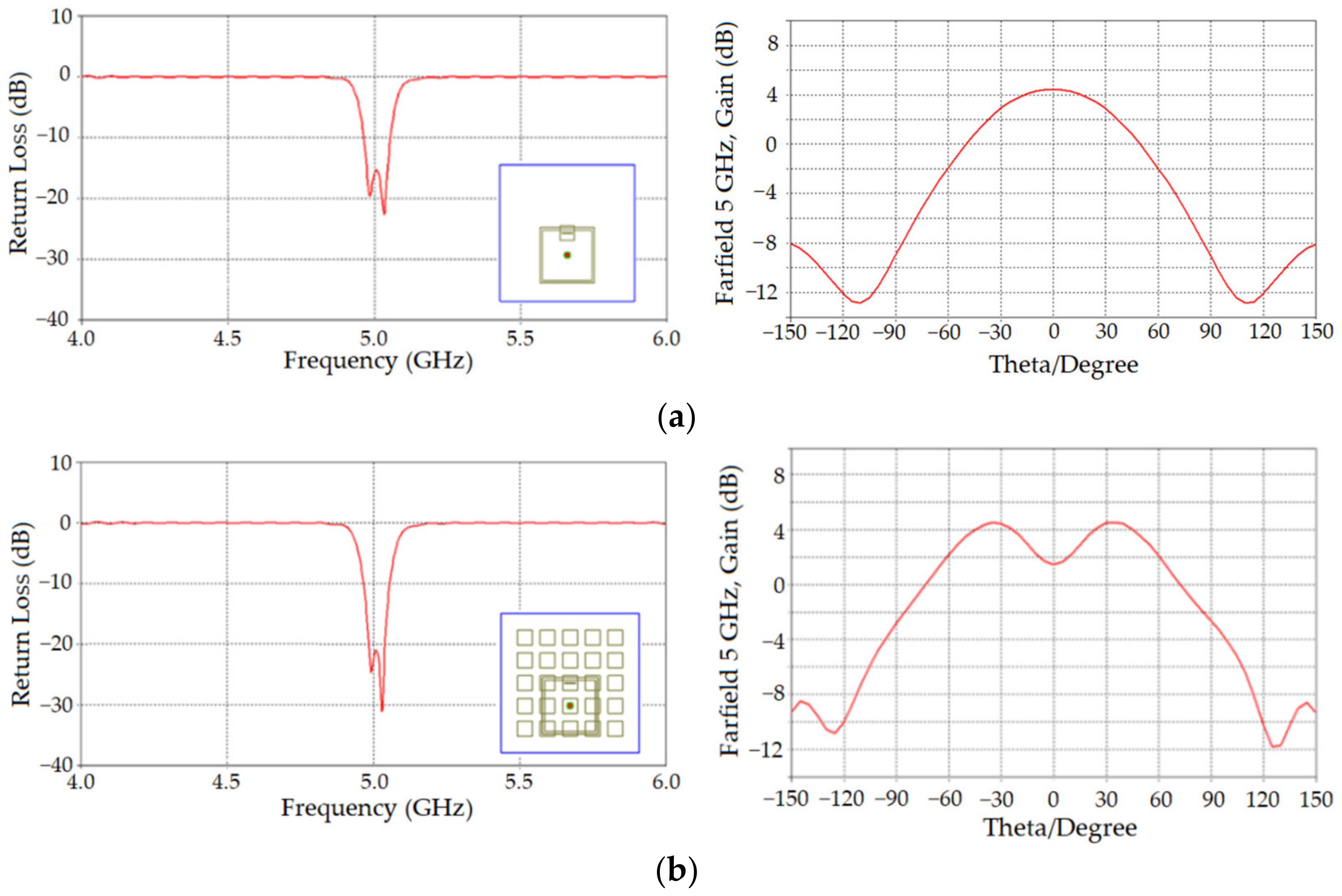
The optimal parameter values of the proposed effects of the installing position antenna are presented in Table 1, and several parameters have been improved thereafter, such as the gain, the return loss, and the beam width. In this section, the various parameters of the proposed antennas were analyzed and simulated. Figure 2 illustrated the measured frequency responses of the single patch and the 5 × 5 square patch array at the operation frequency of 5.0 GHz. It could be seen from Figure 2a that the return loss of the single patch (dy = 18 mm., lp = 11.8 mm., ls = 8.8 mm., ws = 0.5 mm., cx = cy = 40.6 mm., cz = 10 mm., and lf = 6 mm.) was −15 dB. A half-power beam width (HPBW) was ±45°. The bandwidth was 100 MHz at the return loss of −10 dB. Consequently, it could be seen from Figure 2b that the return loss of the 5 × 5 square patch is −22 dB. A half-power beam width (HPBW) was ± 60°. The same bandwidth of 100 MHz at the return loss of −10 dB was, likewise, observed.
Hence, the return loss reduction is improved by using the parasitic patch array antenna with respect to the single patch antenna structure. Since the presence of the parasitic patch array is around the radiated patch (the patch is over the slot at the origin), this ultimately yields a broad-beam radiation pattern.
3.2. Effects of the Installing Position and the Square Patches Length
In general, the effect of the installation position is varied for the position of the rectangular cavity ‘dy’ whereas other parameter values were kept constant. The following parameter values were constrained throughout the experiment: the square patch length ‘lp’, the rectangular slot length ‘ls’, the rectangular slot width ‘ws’, the cavity length ‘cx’, the cavity width ‘cy’, the cavity height ‘cz’, the exciting probe length ‘lf’, and the gap between parasitic patches ‘a’ and ‘b’. Figure 3 shows six cases of the measured variation of the rectangular cavity positions ‘dy’, ranging from 15.0 to 20.0 mm versus the frequency (GHz). It could be seen from Figure 3 when the values of ‘dy’ shifted from the center of the slot along the y-axis, the return loss curve went under the −10 dB line, and the minimal return loss appeared at dy = 18.0 mm, as expected in Table 1.
Similarly, the effect of the installation position and the effects of the square patch length varied according to the lengths of the square patch ‘lp’ whereas other parameter values were kept constant. The following parameter values were constrained throughout the experiment: the position of the rectangular cavity ‘dy’, the rectangular slot length ‘ls’, the rectangular slot width ‘ws’, the cavity length ‘cx’, the cavity width ‘cy’, the cavity height ‘cz’, the exciting probe length ‘lf’, and the gap between parasitic patches ‘a’ and ‘b’. Figure 4 showed five cases of the measured variation of the lengths of the square patch from lp = 9.8 to 13.8 mm versus the frequency (GHz). It could be seen from Figure 4 that the minimal return loss appeared at lp = 11.8 mm, as expected in Table 1. Nonetheless, when the square patch lengths ‘lp’ deviated from 11.8 mm, the return loss values were likely to increase.
3.3. Effects of the Lengths and Widths of the Rectangular Slot
Typically, the effects of the rectangular slot lengths ‘ls’ varied whereas other parameter values were kept constant. The following parameter values were constrained throughout the experiment: the positions of the rectangular cavity ‘dy’, the square patch length ‘lp’, the rectangular slot width ‘ws’, the cavity length ‘cx’, the cavity width ‘cy’, the cavity height ‘cz’, the exciting probe length ‘lf’, and the gap between parasitic patches ‘a’ and ‘b’. Figure 5 showed six cases of the measured variation of the rectangular slot lengths ls = 8.0 to 9.0 mm versus the frequency (GHz). It could be seen from Figure 5 that the minimal return loss appeared at ls = 8.8 mm as expected in Table 1. However, when the rectangular slot lengths ‘ls’ deviated from 8.8 mm, the return loss value was likely to increase.
Similarly, the rectangular slot length and the effects of the rectangular slot width varied according to the rectangular slot width ‘ws’ whereas other parameter values were kept constant. The following parameter values were constrained throughout the experiment: the position of the rectangular cavity ‘dy’, the square patch length ‘lp’, the rectangular slot length ‘ls’, the cavity length ‘cx’, the cavity width ‘cy’, the cavity height ‘cz’, the exciting probe length ‘lf’, and the gap between parasitic patches ‘a’ and ‘b’. Figure 6 showed six cases of the measured variation of the rectangular slot of widths ‘ws’, ranging from 0.3 to 1.3 mm versus the frequency (GHz). It could be seen from Figure 6 that the minimal return loss appeared at ws = 0.5 mm, as expected in Table 1. However, when the rectangular slot of width ‘ws’ deviated from 0.5 mm, the return loss value was likely to increase.
3.4. Effects of the Dominant Mode (TE101) of the Rectangular Cavity Dimensions
Normally, the effects of the dominant mode (TE101) of the rectangular cavity dimensions vary according to the rectangular cavity dimensions ‘cx’ = ‘cy’ whereas other parameters are fixed. The following parameter values are fixed: the positions of the rectangular cavity ‘dy’, the square patch length ‘lp’, the rectangular slot length ‘ls’, the rectangular slot width ‘ws’, the cavity height ‘cz’, the exciting probe length ‘lf’, and the gap between parasitic patches ‘a’ and ‘b’. Figure 7 shows five cases of the measured variation of the rectangular cavity dimensions ‘cx = cy’, ranging from = 40.2 to 41.0 mm versus the frequency (GHz). It could be seen from Figure 7 that the minimal return loss appeared at cx = cy = 40.6 mm, as expected in Table 1. Nevertheless, when the rectangular cavity dimension ‘cx’ = ‘cy’ deviated from 40.6 mm, the return loss value was likely to increase.
Similarly, the rectangular cavity dimension ‘cx’ = ‘cy’ and the effects of another dominant mode (TE101) dimension varied according to the rectangular cavity dimension with height ‘cz’ whereas other parameter values were kept constant. The following parameter values were constrained throughout the experiment: the position of the rectangular cavity ‘dy’, the square patch length ‘lp’, the rectangular slot length ‘ls’, the rectangular slot width ‘ws’, the dominant mode (TE101) of the rectangular cavity dimension ‘cx’ = ‘cy’, the exciting probe length ‘lf’, and the gap between parasitic patches ‘a’ and ‘b’. Figure 8 showed five cases of the measured variation of the rectangular cavity dimensions with height cz, ranging from 9.0 to 11.0 mm versus the frequency (GHz). It could be seen from Figure 8 that the minimal return loss appeared at cz = 10.0 mm, as expected in Table 1. Nevertheless, when the rectangular cavity dimension with height cz deviated from 10.0 mm, the return loss value was likely to increase.
3.5. Effects of the Exciting Probe and the Gap between Parasitic Patches
Consequently, the effects of the exciting probe varied according to the exciting probe length ‘lf’ whereas other parameter values were kept constant. The following parameter values were constrained throughout the experiment: the position of the rectangular cavity ‘dy’, the square patch length ‘lp’, the rectangular slot length ‘ls’, the rectangular slot width ‘ws’, the cavity length ‘cx’, the cavity width ‘cy’, the cavity height ‘cz’, and the gap between parasitic patches ‘a’ and ‘b’. Figure 9 shows five cases of the measured variation of the exciting probe length, ranging from lf = 4.0 to 8.0 mm versus the frequency (GHz). It could be seen from Figure 9 that the minimal return loss appeared at lf = 6.0 mm, as expected in Table 1. Nonetheless, when the exciting probe length ‘lf’ deviated from 6.0 mm, the return loss value was likely to increase.
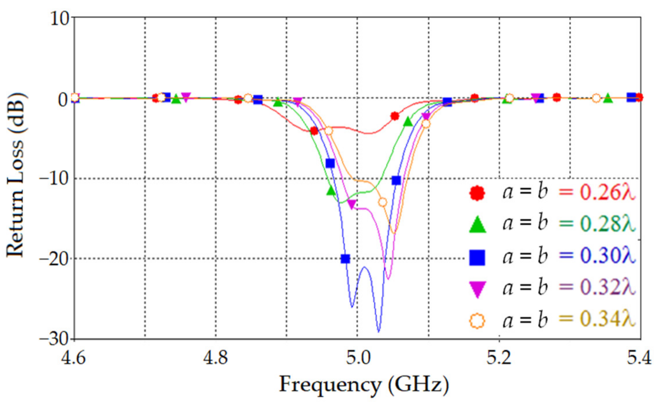
Similarly, the exciting probe length and the effects of the gap between parasitic patches varied according to the gap between parasitic patches ‘a’ = ‘b’ whereas other parameter values were kept constant. The following parameter values were constrained throughout the experiment: the position of the rectangular cavity ‘dy’, the square patch length ‘lp’, the rectangular slot length ‘ls’, the rectangular slot width ‘ws’, the cavity length ‘cx’, the cavity width ‘cy’, the cavity height ‘cz’, and the exciting probe length ‘lf’. Figure 10 showed five cases of the measured variation of the gap between parasitic patches from a = b = 0.26λ to 0.34λ mm versus the frequency (GHz). It could be seen from Figure 10 that the minimal return loss appeared at a = b = 0.30λ mm as expected in Table 1. However, when the gap between parasitic patches ‘a’ = ‘b’ deviated from 0.30λ mm, the return loss value was likely to increase.
3.6. Simulated Radiation Patterns
The radiation pattern of the proposed antenna in Figure 1 was simulated in terms of the gain (dB) as well as E-plane and H-plane patterns. This simulation was based on the varied gap between parasitic patches ‘a’ and ‘b’ whereas other parameters are fixed as shown in Table 1.
Figure 11 showed seven cases of the measured variation of the gap between parasitic patches ‘a’ = ‘b’ = nλ from 0.2λ to 0.3λ versus the degree. It could be seen from Figure 11 that the wide beam and the earth match beam radiation, showing the gap between the parasitic patch array was nλ = 0.3λ. Figure 12 and Figure 13 showed the simulated E-plane and H-plane patterns of the proposed antenna in Figure 1 of the configuration parameters in Table 1. It could be seen from Figure 12 and Figure 13 that the radiation pattern of the proposed antenna could produce the half-power beam width of the E-plane and H-plane around 130° and 80°, respectively.
4. Experimental Results and Discussions
The effect of the patch array has been shown in Figure 2b; the proposed antenna was fabricated on a 100 mm × 100 mm double-sided FR4 epoxy. This antenna was the 5 × 5 microstrip patch parasitic array using a cavity-backed slot. The experimental results were measured with the Agilent E5071C ENA network analyzer and compared to those of the simulation. Figure 14 showed the measured return loss of the antenna prototype. It could be seen from Figure 14 that the minimal return loss of −22.497 dB appeared at 5.0 GHz. Figure 15 showed the comparison of the measured and simulated results in terms of the return loss (dB) versus the frequency (GHz). It could be seen from Figure 15 that the return loss and the operating bandwidth with −10 dB of the return loss are −22.49 dB and 40 MHz (4.97–5.02 GHz), respectively. These were corresponding to an impedance bandwidth of 1% in respect to the center frequency of 5.0 GHz. Therefore, the measured and simulated results successfully met the requirements for the return loss.
Although the measured return loss seemed to be a narrower bandwidth over the simulated outcomes, these discrepancies were due to the following: the fabrication tolerances of the related physical parameter, the position of the cavity-backed slot coupling, the uncertainty of the thickness and/or the dielectric constant of the FR4 substrate, and the effects of improper soldering of the cavity and SMA connectors that are used in material characterization and microwave devices [31]. Figure 16a,b showed the measured and simulated values in the E-plane (y-z plane) and H-plane (x-y plane) at 5.0 GHz. with far-field normalized radiation patterns. These radiation patterns of the proposed antenna were measured with the HP 8722D Network Analyzer in an anechoic chamber. The obtained radiation patterns have directional radiations in the E-plane and H-plane of half-power beam widths around ± 65° and ± 40°, respectively. The maximum directive gain of the proposed antenna computed by applying the Friis Transmission Equation [32] was approximately 5.6 dB. The measured front-to-back ratios in comparison with the simulated one of E-plane radiation patterns were 30 and 16 dB, respectively while the simulated ones of H-plane radiation patterns were 22 and 14 dB, respectively.
5. Conclusions
A broad-beam antenna using a microstrip patch parasitic array, which is excited by the cavity-backed slot coupling, has been proposed in this paper. In order to achieve the broad-beam antenna, the square patch sizes, the slot length, the slot width, the probe length, the cavity positions, and the gaps between the parasitic patches array around the radiation patch were simulated. The key characteristics, especially the return loss and radiation patterns, were acquired with the assistance of the CST software. Measurements of the fabricated antenna have shown that the proposed antenna has a gain of 5.6 dB and the half-power beam widths of 130° and 80° in E-plane and H-plane, respectively. The return loss of the antenna at the operating frequency (at 5.0 GHz) is approximately −22.39 dB. Consequently, the antenna can be promisingly applied in LEO satellite for an earth coverage beam or could be used for other applications in the wireless communications system, such as WLAN and sub-6 GHz 5G communications.
Author Contributions
Conceptualization, T.P. and W.S.-N.; methodology, T.P. and W.S.-N.; software, T.P. and W.S.-N.; validation, T.P. and W.S.-N.; formal analysis, T.P. and W.S.-N.; investigation, T.P. and W.S.-N.; resources, T.P. and W.S.-N.; data curation, T.P. and W.S.-N.; writing—original draft preparation, T.P. and W.S.-N.; writing—review and editing, W.S.-N.; visualization, T.P. and W.S.-N.; supervision, W.S.-N.; project administration, W.S.-N.; funding acquisition, T.P. and W.S.-N. All authors have read and agreed to the published version of the manuscript.
Funding
This research project was financially supported by Mahasarakham University, Kantarawichai, Maha Sarakham, Thailand. The grant number is 5801008.
Institutional Review Board Statement
Not applicable.
Informed Consent Statement
Not applicable.
Data Availability Statement
The data presented in this study are available on request from the authors.
Acknowledgments
The research project was supported by Rajamangala University of Technology Isan, Thailand.
Conflicts of Interest
The authors declare no conflict of interest.
References
- Sonasang, S.; Angkawisittpan, N. Design of microstrip parallel-coupled lines with high directivity using symmetric-centered inductors. Appl. Comput. Electromagn. Soc. J. 2021, 36, 657–663. [Google Scholar] [CrossRef]
- Jamsai, M.; Angkawisittpan, N.; Nuan-On, A. Design of a compact ultra-wideband bandpass filter using inductively compensated parallel-coupled lines. Electronics 2021, 10, 2575. [Google Scholar] [CrossRef]
- Angkawisittpan, N.; Siritaratiwat, A. A dual frequency monopole antenna with double spurlines for PCS and bluetooth applications. Appl. Comput. Electromagn. Soc. J. 2016, 31, 976–981. [Google Scholar]
- Chakma, N.; Farhad, M.M.; Islam, A.J.; Chakraborty, S.; Nesar, M.S.B.; Muktadir, M.A. Performance Analysis of a Microstrip Patch Antenna for Satellite Communications at K Band. In Proceedings of the 21st International Conference of Computer and Information Technology (ICCIT), Dhaka, Bangladesh, 21–23 December 2018; pp. 1–4. [Google Scholar]
- Borel, T.T.S.; Yadav, A.R.; Shah, U. Design of Rectangular Patch Array Antenna for Satellite Communication. In Proceedings of the 3rd International Conference on Computing Methodologies and Communication (ICCMC), Erode, India, 27–29 March 2019; pp. 759–764. [Google Scholar]
- Mahatmanto, B.P.A.; Apriono, C. High Gain 4 × 4 Microstrip Rectangular Patch Array Antenna for C-Band Satellite Applications. In Proceedings of the FORTEI-International Conference on Electrical Engineering (FORTEI-ICEE), Bandung, Indonesia, 23–24 September 2020; pp. 125–129. [Google Scholar]
- Harane, M.M.; Ammor, H. Design & Development of 2 × 4 Microstrip Patch Antenna Array with Circular Polarized Elements for Satellite Application. In Proceedings of the International Symposium on Advanced Electrical and Communication Technologies (ISAECT), Rabat, Morocco, 21–23 November 2018; pp. 1–4. [Google Scholar]
- Hay, S.G.; Bateman, D.G.; Bird, T.S.; Cooray, F.R. Simple Ka-band earth coverage antenna for LEO satellite. IEEE Antennas Propag. Soc. Int. Symp. 1999, 1, 11–16. [Google Scholar]
- Trivino, I.V.; Skrivervik, A.K. Broad-beam microstrip patch antenna using higher order modes. In Proceedings of the 13th European Conference on Antennas and Propagation (EuCAP), Krakow, Poland, 31 March–5 April 2019; pp. 1–4. [Google Scholar]
- Dou, L.; Li, S.; Cao, W. Research of Wide Beam Antenna. In Proceedings of the International Symposium on Antennas and Propagation (ISAP), Xi’an, China, 27–30 October 2019; pp. 1–3. [Google Scholar]
- Yu, C.A.; Chin, K.S.; Lu, R. 24-GHz Wide-Beam Patch Antenna Array Laterally Loaded With Parasitic Strips. In Proceedings of the 2019 Cross Strait Quad-Regional Radio Science and Wireless Technology Conference (CSQRWC), Taiyuan, China, 18–21 July 2019; pp. 1–3. [Google Scholar]
- Marcano, N.J.; Bartle, H.H.; Jacobsen, R.H. Patch Antenna Arrays Beam Steering for Enhanced LEO Nano-satellite Communications. In Proceedings of the 2020 IEEE Wireless Communications and Networking Conference (WCNC), Seoul, Korea, 25–28 May 2020; pp. 1–6. [Google Scholar]
- Smulders, P.F.M.; Khusial, S.; Herben, H.A.J. A shaped reflector antenna for 60- GHz indoor wireless LAN access points. IEEE Trans. Vehicular Tech. 2001, 50, 584–591. [Google Scholar] [CrossRef]
- Gupta, R.C.; Sagi, S.K.; Mahajan, M.B. Rotationally Symmetric Shaping of Center-Fed Reflector Antenna For GEO Communication Collocated Small-sized Spacecraft. In Proceedings of the IEEE Indian Conference on Antennas and Propagation (InCAP), Hyderabad, India, 16–19 December 2018; pp. 1–4. [Google Scholar]
- Krachodnok, P.; Wongsan, R. Design of broad-beam microstrip reflectarray. WSEAS Trans. Commun. 2008, 7, 180–187. [Google Scholar]
- Anguix, S.; Araghi, A.; Khalily, M.; Tafazolli, R. Reflectarray Antenna Design for LEO Satellite Communications in Ka-band. In Proceedings of the 15th European Conference on Antennas and Propagation (EuCAP), Dusseldorf, Germany, 22–26 March 2021; pp. 1–5. [Google Scholar]
- Jassim, A.M.; Hristov, H.D. Cavity feed technique for slot coupled microstrip patch array antenna. IEE Proc. Micro. Antennas Prop. 1995, 142, 452–456. [Google Scholar] [CrossRef]
- Puklibmoung, T.; Krachodnok, P.; Wongsan, R. Analysis Design of Broad-Beam MSA Array Using Cavity Back Slot-Coupling. In Proceedings of the International Symposium on Antenna and Propagation (ISAP 2010), Macao, China, 23–26 November 2010; pp. 695–698. [Google Scholar]
- Puklibmoung, T.; Krachodnok, P.; Wongsan, R. A Broad-Beam Antenna Using Nonuniform MSA Parasitic Array Excited by Cavity-Backed Slot. In Proceedings of the International Symposium on Antenna and Propagation (ISAP 2011), JeJu, Korea, 25–28 October 2011; pp. 1–4. [Google Scholar]
- Shin, J.; Yoon, K.; Chung, M.; Lee, S.; Kim, C. Design of a cavity-backed patch antenna for a phased array. In Proceedings of the International Symposium on Antennas and Propagation (ISAP 2018), Busan, Korea, 23–26 October 2018; pp. 727–728. [Google Scholar]
- Vaish, A.; Singh, M.; Kaur, S.; Kumar, P. Design and Analysis of Square microstrip patch Antenna with and without cavity backing. In Proceedings of the International Conference on Inventive Systems and Control (ICISC 2019), Coimbatore, India, 10–11 January 2019; pp. 650–655. [Google Scholar]
- Chadram, S.; Engineer, D. A 16 × 8 Cavity Backed Patch Antenna Array for a Phased Array Radar. In Proceedings of the IEEE Indian Conference on Antennas and Propagation (InCAP), Ahmedabad, India, 19–22 December 2019; pp. 1–5. [Google Scholar]
- Lertwiriyaprapa, T.; Phongcharoenpanich, C.; Kosulvit, S.; Krairiksh, M. Analysis of impedance characteristics of a probe fed rectangular cavity-backed slot antenna. IEEE Trans. Antennas Propagate 2001, 1, 576–579. [Google Scholar]
- Ngobese, B.; Kumar, P. A high gain microstrip patch array for 5 GHz WLAN applications. Adv. Electromagn. 2018, 7, 93–98. [Google Scholar] [CrossRef] [Green Version]
- Al-Hiti, A. Design of rectangular microstrip patch antenna for WLAN and WiMAX applications. J. Eng. Appl. Sci. 2019, 14, 433–438. [Google Scholar]
- Sathishkumar, N.; Arthika, S.; Indhu, G.; Elakkiya, K. Design and Study of Rectangular Micro strip Patch Antenna for WLAN Applications. Int. J. Adv. Sci. Technol. 2020, 29, 3554–3558. [Google Scholar]
- Yerlikaya, M.; Gultekin, S.; Uzer, D. A novel design of a compact wideband patch antenna for sub-6 GHz fifth-generation mobile systems. Int. Adv. Res. Eng. J. 2020, 4, 129–133. [Google Scholar] [CrossRef]
- Khan, J.; Ullah, S.; Tahir, F.A.; Tubbal, F.; Raad, R. A Sub-6 GHz MIMO Antenna Array for 5G Wireless Terminals. Electronics 2021, 10, 3062. [Google Scholar] [CrossRef]
- Al-Gburi, A.; Ibrahim, I.; Zakaria, Z. Wideband Microstrip Patch Antenna for Sub 6 GHz and 5G Applications. Prz. Elektrotechniczny 2021, 11, 26–29. [Google Scholar] [CrossRef]
- CST Studio Suite. Electromagnetic Field Simulation Software, Version 2021; Dassault Systèmes SE: Waltham, MA, USA, 2021. [Google Scholar]
- Nuan-On, A.; Angkawisittpan, N.; Piladaeng, N.; Soemphol, C. Design and Fabrication of Modified SMA-Connector Sensor for Detecting Water Adulteration in Honey and Natural Latex. Appl. Syst. Innov. 2022, 5, 4. [Google Scholar] [CrossRef]
- Balanis, C.A. Antenna Theory Analysis and Design, 4th ed.; John Wiley and Sons: New York, NY, USA, 2016. [Google Scholar]
Figure 1.
The configuration of the proposed antenna: (a) top view; (b) perspective view; (c) photograph of the fabricated antenna design.
Figure 1.
The configuration of the proposed antenna: (a) top view; (b) perspective view; (c) photograph of the fabricated antenna design.


Figure 2.
Simulated return loss and gain pattern of the proposed antenna with the parameters’ value in Table 1: (a) single patch; (b) 5 × 5 patches array.
Figure 2.
Simulated return loss and gain pattern of the proposed antenna with the parameters’ value in Table 1: (a) single patch; (b) 5 × 5 patches array.

Figure 3.
Simulated return loss for different values of ‘dy’.

Figure 4.
Simulated return loss for different values of ‘lp’.

Figure 5.
Simulated return loss for different values of ‘ls’.

Figure 6.
Simulated return loss for different values of ‘ws’.

Figure 7.
Simulated return loss for different values of ‘cx’ and ‘cy’.

Figure 8.
Simulated return loss for different values of ‘cz’.

Figure 9.
Simulated return loss for different values of ‘lf’.

Figure 10.
Simulated return loss for different values of ‘a’ and ‘b’.

Figure 11.
Simulated radiation pattern for different values of the gap between the parasitic patches ‘a = b = nλ’.
Figure 11.
Simulated radiation pattern for different values of the gap between the parasitic patches ‘a = b = nλ’.

Figure 12.
Simulated radiation pattern E-plane at 5.0 GHz.

Figure 13.
Simulated radiation pattern H-plane at 5.0 GHz.

Figure 14.
Measurement returns loss of an antenna prototype.

Figure 15.
Comparison between the measured and the simulated return losses.

Figure 16.
Comparison between the measured and the simulated normalized radiation pattern at 5.0 GHz: (a) E-plane (y-z plane); (b) H-plane (x-z plane).
Figure 16.
Comparison between the measured and the simulated normalized radiation pattern at 5.0 GHz: (a) E-plane (y-z plane); (b) H-plane (x-z plane).


Table 1.
The values of the optimal design parameters of the proposed antenna.
| Parameters | dy | lp | ls | ws | cx | cy | cz | lf | a | b |
| Values (mm) | 18 | 11.8 | 8.8 | 0.5 | 40.6 | 40.6 | 10 | 6 | 0.3λ | 0.3λ |
Publisher’s Note: MDPI stays neutral with regard to jurisdictional claims in published maps and institutional affiliations. |
© 2022 by the authors. Licensee MDPI, Basel, Switzerland. This article is an open access article distributed under the terms and conditions of the Creative Commons Attribution (CC BY) license (https://creativecommons.org/licenses/by/4.0/).
Share and Cite
MDPI and ACS Style
Puklibmoung, T.; Sa-Ngiamvibool, W. Design and Fabrication of Broad-Beam Microstrip Antenna Using Parasitic Patches and Cavity-Backed Slot Coupling. Appl. Syst. Innov. 2022, 5, 31. https://0-doi-org.brum.beds.ac.uk/10.3390/asi5020031
AMA Style
Puklibmoung T, Sa-Ngiamvibool W. Design and Fabrication of Broad-Beam Microstrip Antenna Using Parasitic Patches and Cavity-Backed Slot Coupling. Applied System Innovation. 2022; 5(2):31. https://0-doi-org.brum.beds.ac.uk/10.3390/asi5020031
Chicago/Turabian StylePuklibmoung, Thana, and Worawat Sa-Ngiamvibool. 2022. "Design and Fabrication of Broad-Beam Microstrip Antenna Using Parasitic Patches and Cavity-Backed Slot Coupling" Applied System Innovation 5, no. 2: 31. https://0-doi-org.brum.beds.ac.uk/10.3390/asi5020031