
Design of Refractive/Diffractive Hybrid Projection Lens for DMD-Based Maskless Lithography


1
School of Physics and Optoelectronic Engineering, Guangdong University of Technology, Guangzhou 510006, China
2
Guangdong Provincial Key Laboratory of Information Photonics Technology, Guangdong University of Technology, Guangzhou 510006, China
*
Author to whom correspondence should be addressed.
Optics 2021, 2(2), 103-112; https://0-doi-org.brum.beds.ac.uk/10.3390/opt2020011
Submission received: 13 March 2021
/
Revised: 18 May 2021
/
Accepted: 31 May 2021
/
Published: 8 June 2021
(This article belongs to the Special Issue Fabrication and Applications of Photonic Micro-Devices)
Abstract
:The projection lens is the core component of DMD-based maskless lithography and its imaging quality directly affects the transferal of exposure pattern. Based on the traditional projection lens system, we have designed diffractive optical element (DOE) and aspheric surfaces to optimize the refractive/diffractive hybrid projection lens system to improve its imaging quality. We found that the best effect is obtained when DOE is very close to the front lens group before the diaphragm of the hybrid system. Compared with the traditional projection lens system, this hybrid projection lens system has lower wave aberration with the help of DOE, and higher image quality owing to the modulation transfer function (MTF) value being improved. Finally, a hybrid projection lens system with working distance of 29.07 mm, image Space NA of 0.45, and total length of 196.97 mm is designed. We found that the maximum distortion and field curvature are 1.36 × 10⁻⁵% and 0.91 μm, respectively.
1. Introduction
At present, the manufacturing methods of micro scale complex structures include electron beam lithography [1,2,3], ultra precision machining technology [4], femtosecond laser induced two photo polymerization technology [5], focused ion beam lithography [6,7], excimer laser lithography [8,9], etc. However, these manufacturing methods are complex, have long manufacturing cycle, and high cost. In recent years, a real-time maskless lithography based on digital micromirror device (DMD) has been used to fabricate the optical microstructures required by different applications, because it uses a DMD instead of physical masks as virtual masks and can have rapid prototyping [10,11,12]. The DMD, which is controlled by computer, consists of 1024 × 768 micro-mirrors of 10.8 μm and each micro-mirror can switch into two conditions, ±12° corresponding to the “on” and “off” conditions. The DMD-based maskless lithography system is mainly composed of an illumination optical system, a DMD, and a projection lens system. The projection lens system is the key subsystem of DMD-based lithography [13], which directly determines the imaging quality.
For projection lithography, in order to further improve the resolution of the optical system, researchers need to use shorter wavelength light source and optical objective with larger numerical aperture (NA), as well as resolution enhancement technology (RET) [14], etc. In the design of projection lithography objectives, the NA of the projection objective can be increased by increasing the number of lenses, using special optical materials [15], adopting a catadioptric optical system [16,17,18], using free-form surfaces [19] and aspheric surfaces [20,21], using immersion lithography technology [22,23], etc.
Combining the diffractive optical element with the traditional refractive optical element, the curved surface of the traditional refractive element provides most of the focusing function, and then uses the high-precision arbitrary phase distribution of the diffractive optical element to modulate the optical front and correct various aberrations [24,25,26,27]. It can optimize the projection lens system structure, improve the imaging quality, and make the optical design have more freedom.
In this paper, we have designed a refractive/diffractive hybrid projection lens system for DMD-based maskless lithography by using the combination of a single layer DOE and an aspheric surface, achieving a working distance of 29.07 mm, image Space NA of 0.45, and 196.97-mm long lens. Compared with the traditional projection lens system, this hybrid projection lens system has lower wave aberration, higher image quality and MTF value. The design of the DOE is especially described in detail, and its diffraction efficiency was evaluated. Finally, optimization and analysis was performed on a Zemax software and we will prove that the optimized hybrid projection lens system has higher MTF values and better geometric aberration than the traditional optical systems.
2. DMD-Based Maskless Lithography System and Diffraction Efficiency of DOE
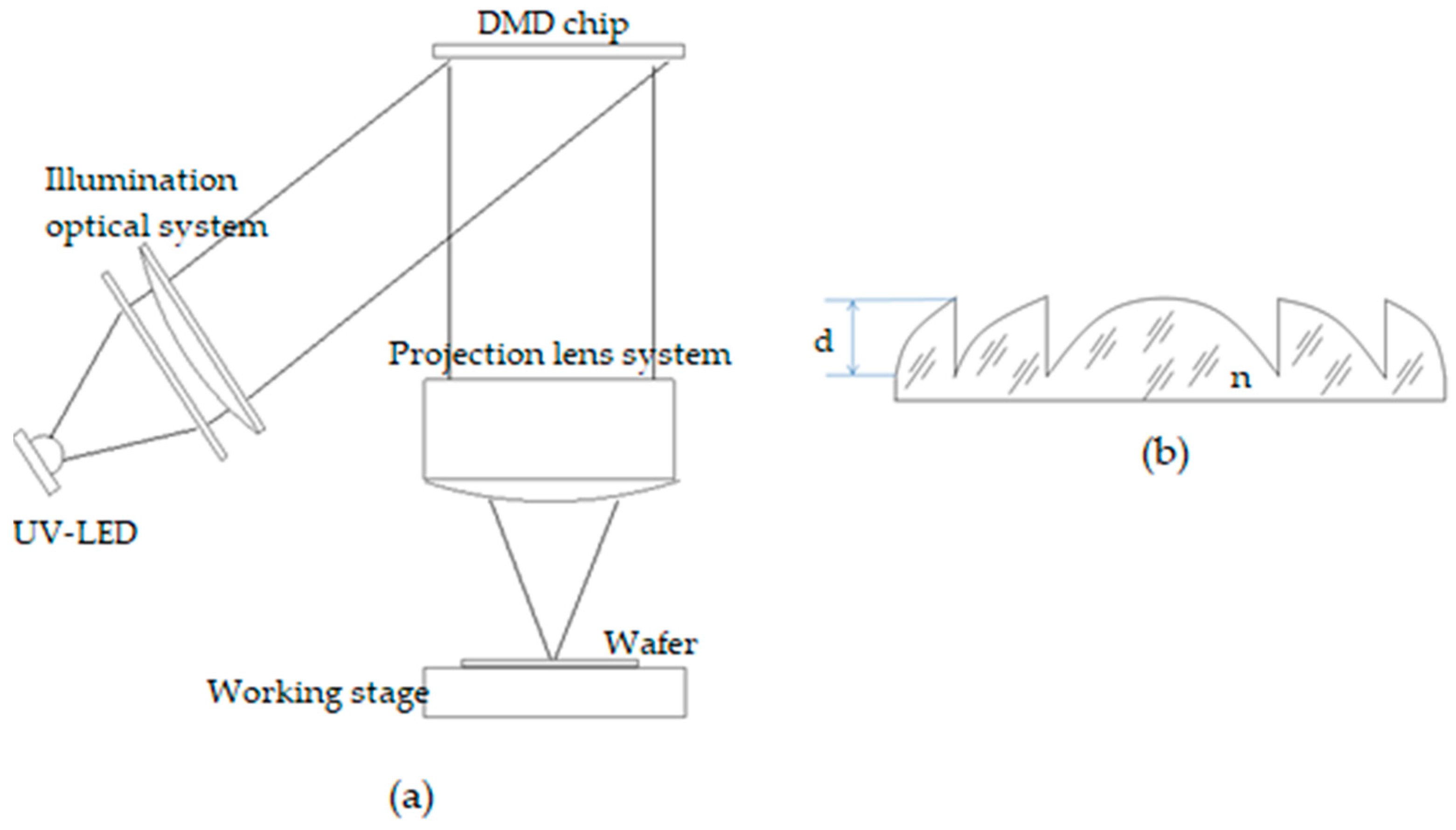
Figure 1a is a simplified structure of the DMD-based maskless lithography system. The light emitted by ultraviolet light-emitting diode (UV-LED) enters the illumination optical system, and is then shaped into a high uniformity of the illumination beam. The exposure light was reflected by DMD, which is controlled by a computer to generate a virtual mask in real time. Light modulated by DMD is imaged by the optical projection lens system into a reduced image, which is projected to the corresponding imaging position of the wafer surface for exposure imaging. The projection lens system is the key subsystem of DMD based lithography, which directly determines the imaging quality. Therefore, it is necessary to improve the imaging quality of the projection system, so as to improve the lithography performance.
where n(λ) is the refractive index of DOE, θ is the incident angle, and d is the depth period of the grating features. When the environment medium is air, n’ = 1. Hence, the m’th order diffraction efficiency of the DOE in the oblique situation can be expressed as:
where sinc(x) = sin(πx)/πx, and m is the diffraction order.
3. Optical Design of Projection Lens Using DOE for DMD-Based Maskless Lithography
3.1. Design Specification
According to the Rayleigh criterion, the resolution of the projection objective is determined by the following formula:
In the above formula, k1 is the process factor, λ is the wavelength of the light source, NA is the numerical aperture of the projection lens group, NA = n∙sinθ, n is the refractive index of the medium between the projection lens group and the wafer, and θ is the maximum incident angle of exposure light on the surface of the wafer. As a design example, a projection lens system using single layer DOE for DMD-based maskless lithography is designed. The DMD used here has the overall size of 11.059 mm × 8.294 mm, which consists of 1024 × 768 micro-mirrors of 10.8 μm, and therefore, when designing projection objective lens, the maximum line field of view equal to 13.8 mm is the diagonal of DMD (here, we assume that the half height of the object is 7 mm). The working wavelength is 403–407 nm, and the primary wavelength is 405 nm. To achieve the minimum line width of 2.16 μm, the magnification of the system must reach β = −2.16/10.8 = −0.2. The distance from the first surface of the projection lens to the DMD plane should be large enough to place the homogenizer and illumination mirror. The design specifications are listed in Table 1.
3.2. Design Process
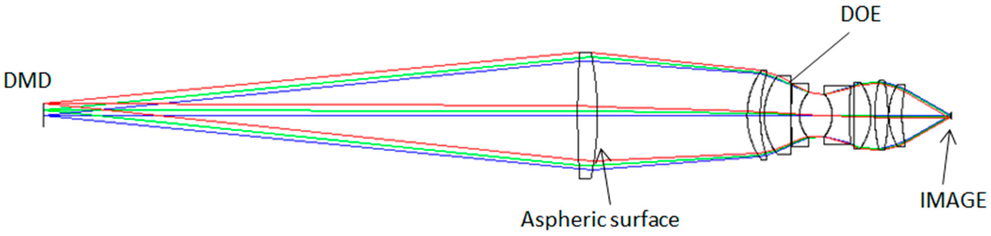
The projection lens of DMD maskless lithography is a telecentric optical system with medium field of view and large relative aperture. We took one suitable refractive projection lens as the starting point of the design process using the optical design software Zemax [29,30]. This projection lens system was an improved structure of double Gaussian objective, which consists of eight refractive lens and the distribution of its refraction power is +,+,+,−, (stop), −,+,+,+. Its magnification and Image Square NA were about −0.2924x and 0.33, respectively, and its minimum line width was 4 μm. In this experiment, a single-layer DOE and an aspheric surface were introduced into the system in order to improve the imaging quality of the projection system, and the minimum line width was optimized to 2.16 μm. After inputting the initial structure data into the Zemax software, we set the radius of curvature and partial thickness of multiple refractive surfaces as variables, and selected the default wave aberration optimization method. Then, we added other operands in the optimization function of Zemax software, such as maximum distortion (DIMX), magnification (PMAG) and so on. In the basically symmetrical optical system, it is preferable to place the DOE adjacent or near the stop. Through continuous trial and optimization in Zemax software, it was found that DOE is set in the sixth surface of the optical system, and the imaging quality was the best. In order to facilitate the manufacture of diffractive optical elements, the material of the third lens was changed to polymethyl methacrylate (PMMA). The final designed structure of the refractive/diffractive hybrid optical system is shown in Figure 2 and Table 2, including seven refractive components, a single layer DOE, and an aspheric surface.
The imaging quality of the optical system can be improved by using aspheric surface and binary surface without adding components. In this study, the even aspheric surface was used, and the sag of the surface was given by:
where z is the sag of the even aspheric surface, c is the curvature, k is the conic constant, and r is the radial coordinate. In the meantime, the aspheric coefficient of diffractive optical element can be used to balance the higher-order aberrations. The binary 2 surface type was used, and it added phase to the ray according to the following polynomial expansion:
where N is the number of polynomial coefficients in the series, Ai is the coefficient on the 2ith power of ρ, which is the normalized radial aperture coordinate, and M is the diffraction order. Table 3 and Table 4 show the detailed data and configuration of polynomial coefficients for binary 2 surfaces and even aspheric surfaces. The depth period of the grating features for the designed wavelength was calculated by d = λ/(nDOE − 1) = 0.405/(1.5065 − 1) = 0.7995 μm in the design. In order to simplify the fabrication, planar substrates were selected as the DOE substrates. The microstructure on PMMA can be fabricated by the single-point diamond turning (SPDT) [31,32] or precision molding process.
3.3. Diffraction Efficiency Analysis of Single Layer DOE
The actual optical transfer function (OTF) of the hybrid optical system can be obtained by calculating the product of the diffraction efficiency of DOE and the MTF curve given by the design software [33]. In the Zemax software, the imaging performances of hybrid systems are computed by the ideal phase function and the effect of incidence angles at DOE are ignored. Therefore, it is necessary to analyze the influence of the incident angle on the diffraction efficiency of DOE. According to the final optimized result of the projection lens of DMD maskless lithography, the range of incident angles of the single layer DOE are from 0° to 26.4°. Figure 3 shows the relationship between diffraction efficiency and incident angle of single-layer DOE calculated by formula 2. It can be seen that the diffraction efficiency of DOE in the whole field of view is more than 87%.
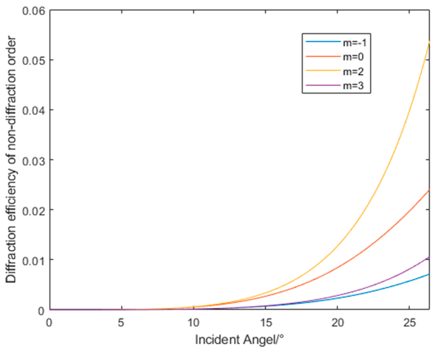
As we know, because of the multiple diffracted orders of DOE, it can produce more than one image and reduce the resolution of the corresponding optical system. Hence, the diffraction efficiency of non-design diffracted orders needs to be analyzed. As shown in Figure 4, the diffraction efficiency of non-design order light in the whole incident angle range is less than 6%, which is acceptable.
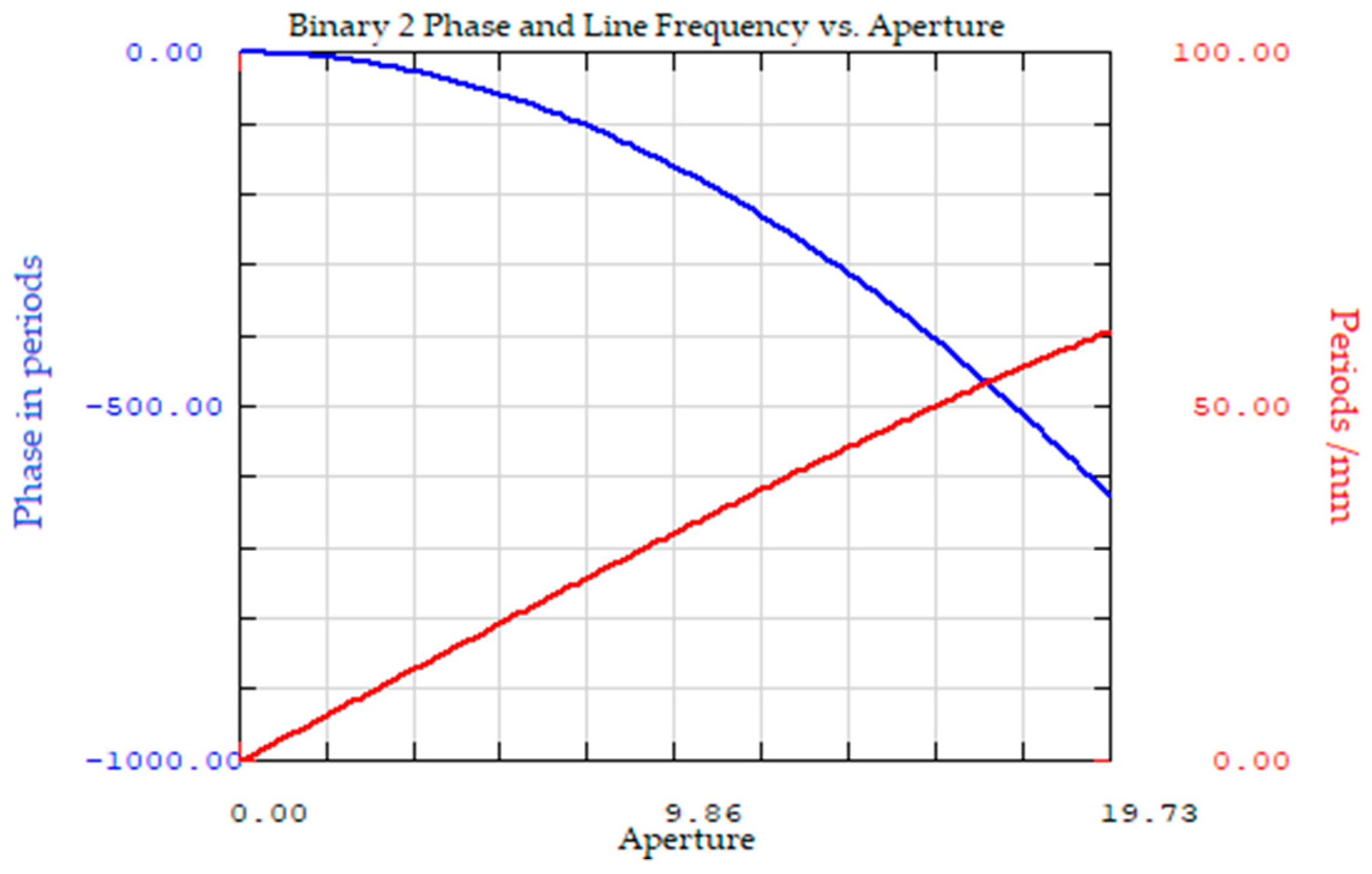
Figure 5 shows the phase plot and the line frequency versus aperture of the binary diffraction surfaces. The maximum line frequency is 60.58 line pairs/mm (lp/mm) and the corresponding width of the minimum period is 16.5 μm. The diffraction efficiency of 95% can be obtained when the number of etching levels is 8.
4. The Comparison of Optical Performance Between Two Projection Lens Systems
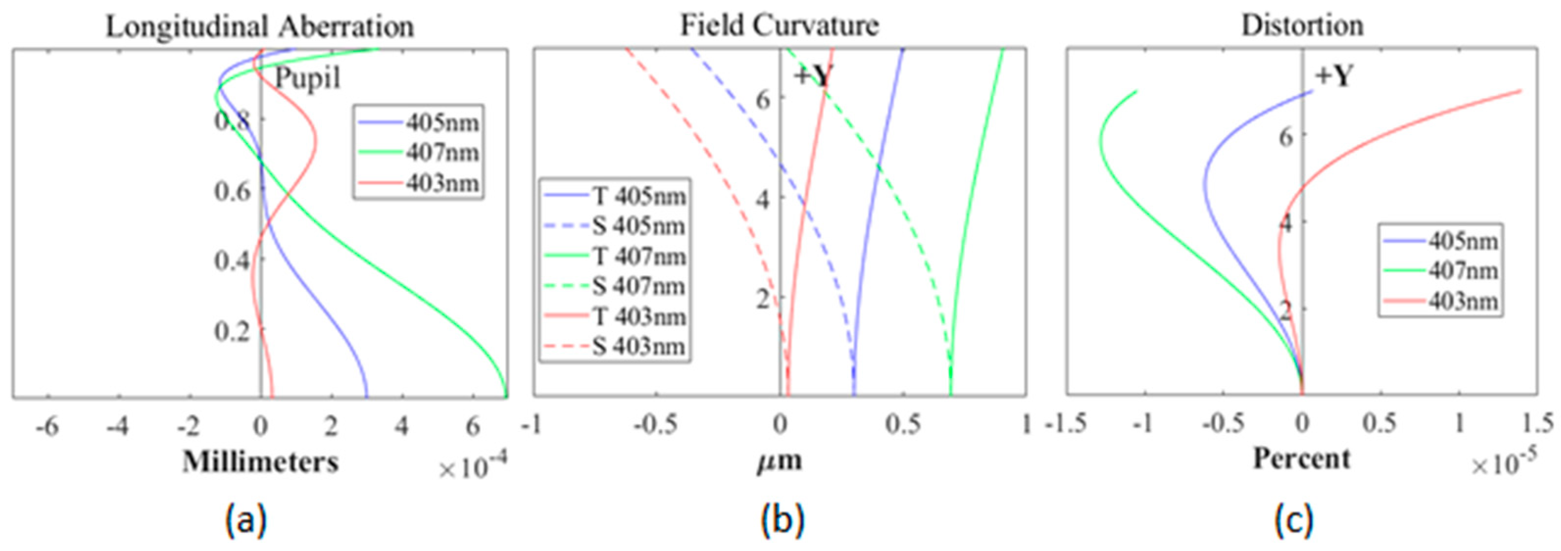
As shown in Figure 6a, the longitudinal aberration of the refractive/diffractive hybrid projection lens system is less than 0.7 μm, and the field curvature is less than 1.0 μm in Figure 6b, and the maximum distortion of the system is less than 1.5 × 10⁻⁵% in Figure 6c, which is very small.
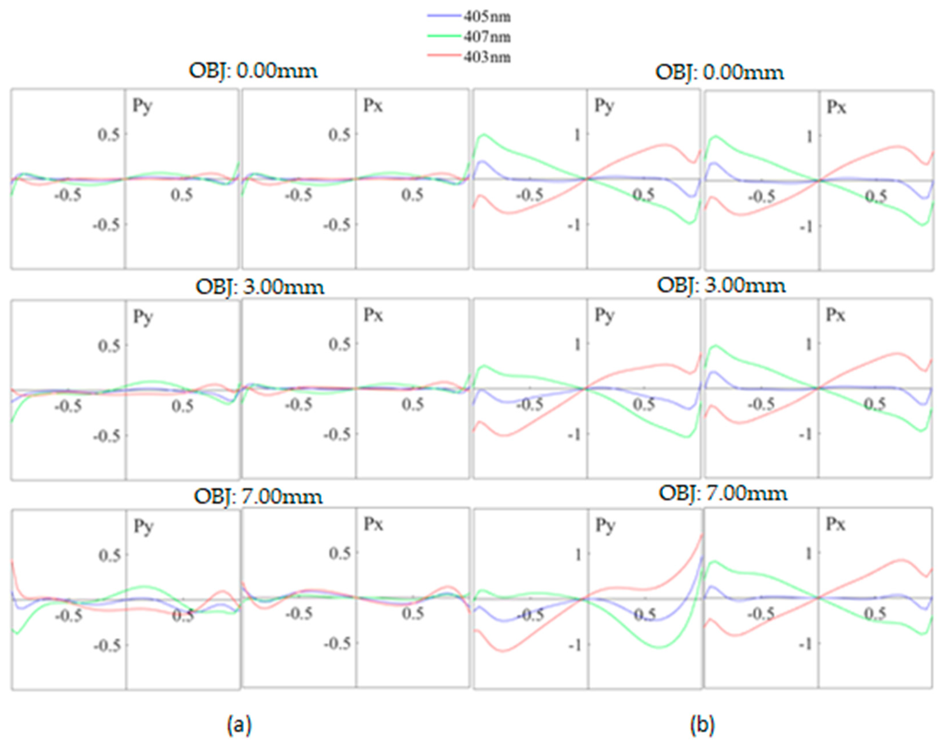
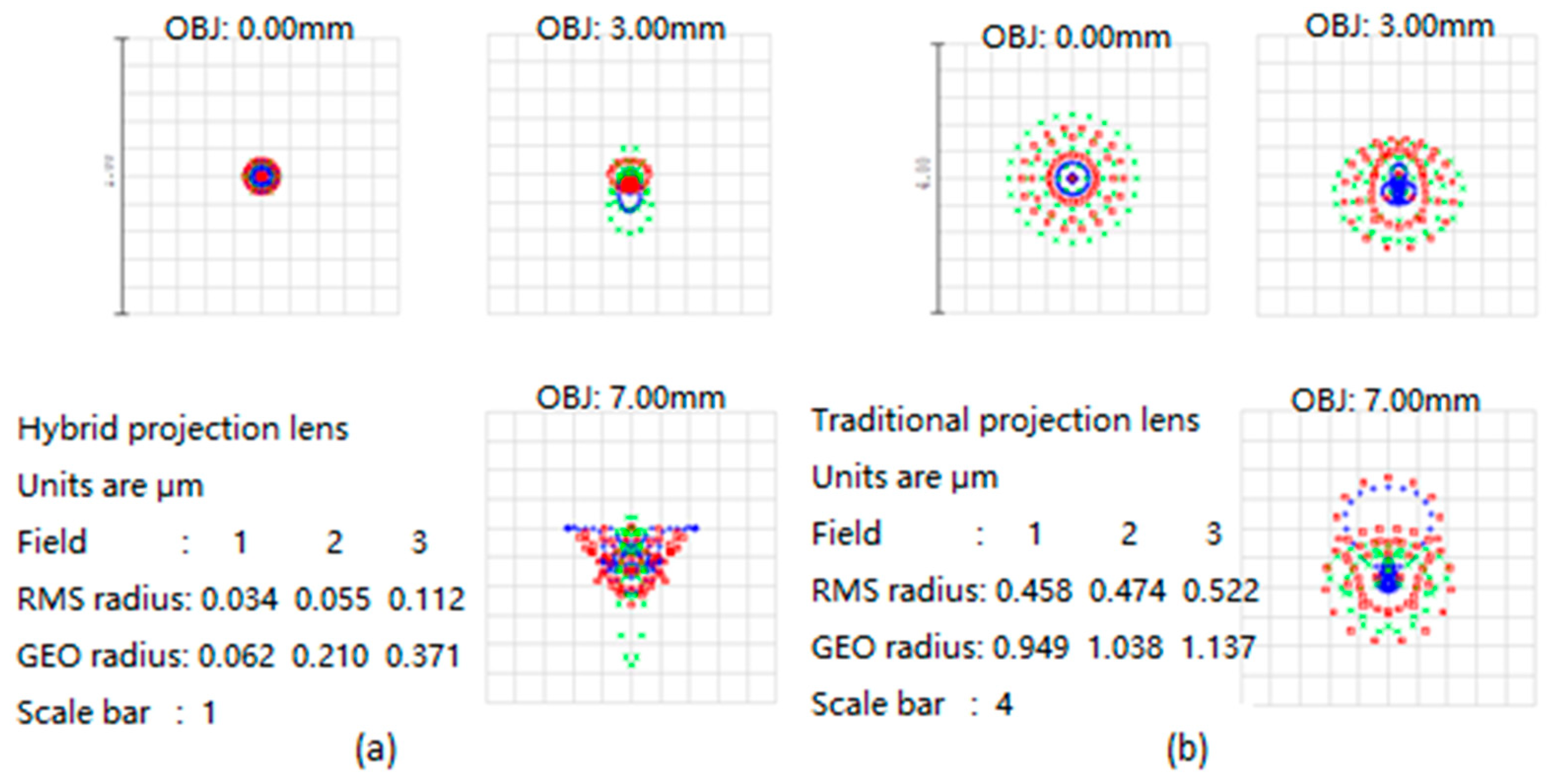
The wave aberrations of traditional refraction system and refractive/diffractive hybrid system for axial field, 0.43 field, and full field on image plane are shown in Figure 7. In this figure, we can see that the axial chromatic aberration is much better in the hybrid system, almost 2 times smaller than for the traditional optical system. The maximum mean square radius of the spot pattern of the hybrid optical system shown in Figure 8 is 0.112 μm, which is much smaller than the 0.522 μm of the traditional optical system. Moreover, we can see that the spherical aberrations, the chromatic aberrations, and comas of the hybrid system are much better corrected than the traditional system.
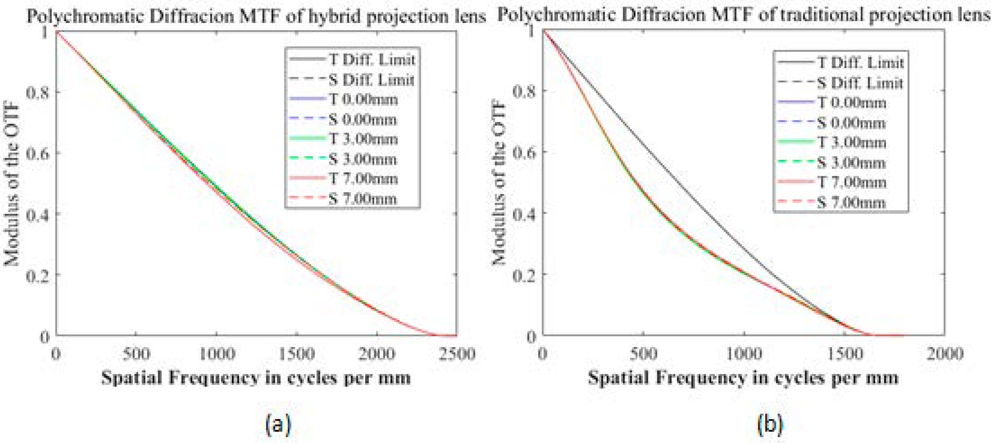
It can be seen from Figure 9a that the MTF curves of all wavelengths and fields of view of the hybrid optical system are almost coincident, and are very close to the diffraction limited ideal curve. As shown in Figure 9a,b, the MTF values of the hybrid system using single layer DOE are higher than those of the traditional refraction system in the high frequency region. The overall MTF modulation is better than 50% at 940 line lp/mm. Based on the above analysis, we can conclude that when a single layer DOE and an aspheric surface are used, the projection lens of DMD-based maskless lithography can provide better resolution and image quality than the traditional refraction system.
5. Conclusions
For a DMD-based maskless lithography projection optical system, we propose a refractive/diffractive hybrid projection lens system by using a single layer DOE and an aspheric surface. Compared with the traditional projection lens system, we found that the wave aberrations of the hybrid projection lens system were diminished, almost 2 times smaller than for the traditional one. The MTF values of the hybrid system were higher than those of the traditional refraction system in the high frequency region and the overall MTF modulation was greater than 50% at 940 lp/mm. Finally, a hybrid projection lens system with working distance of 29.07 mm, image Space NA of 0.45, and total length of 196.97 mm have been designed. The results show that the maximum distortion and field curvature were 1.36 × 10⁻⁵% and 0.91 μm, respectively.
Author Contributions
Methodology, software, formal analysis, writing—original draft preparation, Z.X.; investigation, J.Z.; resources, B.W.; data curation, Z.M.; All authors have read and agreed to the published version of the manuscript.
Funding
This work was funded by Key-Area Research and Development Program of Guangdong Province (2020B090924001) and Guangzhou Science and Technology planning project (202002030210). Corresponding author: Jinyun Zhou (Email: [email protected]).
Conflicts of Interest
The authors declare no conflict of interest.
References
- Vieu, C.; Carcenac, F.; Pépin, A.; Chen, Y.; Mejias, M.; Lebib, A.; Manin-Ferlazzo, L.; Couraud, L.; Launois, H. Electron beam lithography: Resolution limits and applications. Appl. Surface Sci. 2000, 164, 111–117. [Google Scholar] [CrossRef]
- Drost, M.; Tu, F.; Berger, L.; Preischl, C.; Zhou, W.; Gliemann, H.; Wöll, C.; Marbach, H. Surface-Anchored Metal–Organic Frameworks as Versatile Resists for Gas-Assisted E-Beam Lithography: Fabrication of Sub-10 Nanometer Structures. ACS Nano 2018, 12, 3825–3835. [Google Scholar] [CrossRef] [PubMed]
- Jiang, N.; Zarkadoula, E.; Narang, P.; Maksov, A.; Kravchenko, I.; Borisevich, A.; Jesse, S.; Kalinin, S.V. Atom-by-atom fabrication by electron beam via induced phase transformations. MRS Bull. 2017, 42, 653–659. [Google Scholar] [CrossRef]
- Zhang, S.J.; To, S.; Zhu, Z.W.; Zhang, G.Q. A review of fly cutting applied to surface generation in ultraprecision machining. Int. J. Mach. Tools Manuf. 2016, 103, 13–27. [Google Scholar] [CrossRef]
- Hu, Y.; Chen, Y.; Ma, J.; Li, J.; Huang, W.; Chu, J. High-efficiency fabrication of aspheric microlens arrays by holographic femtosecond laser-induced photopolymerization. Appl. Phys. Lett. 2013, 103, 141112. [Google Scholar] [CrossRef]
- Cai, J.; Zhu, Z.; Alkemade, P.F.A.; Veldhoven, E.v.; Wang, Q.; Ge, H.; Rodrigues, S.P.; Cai, W.; Li, W.-D. 3D Volumetric Energy Deposition of Focused Helium Ion Beam Lithography: Visualization, Modeling, and Applications in Nanofabrication. Adv. Mater. Interface 2018, 5, 1800203. [Google Scholar] [CrossRef]
- Henry, M.D.; Shearn, M.J.; Chhim, B.; Scherer, A. Ga+ beam lithography for nanoscale silicon reactive ion etching. Nanotechnology 2010, 21, 245303. [Google Scholar] [CrossRef] [PubMed]
- Lin, B.J. Immersion lithography and its impact on semiconductor manufacturing. J. Microlithogr. Microfabr. Microsyst. 2004, 3, 1–7. [Google Scholar]
- Ogawa, K.; Sasago, M.; Endo, M.; Ishihara, T. A KrF Excimer Laser Lithography for Half Micron Devices. Jpn. J. Appl. Phys. 1988, 27, 1521–1525. [Google Scholar] [CrossRef]
- Biao, Y.; Zhou, J.; Chen, Q.; Lei, L.; Wen, K. Fabrication of hexagonal compound eye microlens array using DMD-based lithography with dose modulation. Opt. Express 2018, 26, 28927–28937. [Google Scholar]
- Zheng, Q.; Zhou, J.; Chen, Q.; Lei, L.; Wen, K.; Hu, Y. Rapid Prototyping of a Dammann Grating in DMD-Based Maskless Lithography. IEEE Photonics J. 2019, 11, 2400410. [Google Scholar] [CrossRef]
- Erdmann, L.H.; Deparnay, A.; Wirth, F.; Brunner, R. MEMS-based lithography for the fabrication of micro-optical components. In Micromachining Technology for Micro-Optics & Nano-Optics II; International Society for Optics and Photonics: San Jose, CA, USA, 2003; Volume 5347, pp. 79–84. [Google Scholar]
- Chen, R.H.; Liu, H.; Zhang, H.L.; Zhang, W.J.; Xu, J.; Xu, W.B.; Li, J.H. Edge smoothness enhancement in DMD scanning lithography system based on a wobulation technique. Opt. Express 2017, 25, 21958–21968. [Google Scholar] [CrossRef]
- Levenson, M.D. Using Destructive Optical Interference in Semiconductor Lithography. Opt. Photonics News 2006, 17, 30–35. [Google Scholar] [CrossRef]
- Bel’skiĭ, A.B.; Gan, M.A.; Mironov, I.A.; Seĭsyan, R.P. Prospects for the development of optical systems for nanolithography. J. Opt. Technol. 2009, 76, 496–503. [Google Scholar] [CrossRef]
- Liu, F.; Li, Y. Initial structure design of coaxial six–ten mirror central-obscured extreme ultraviolet lithographic objective. Appl. Opt. 2014, 53, 6444–6451. [Google Scholar] [CrossRef] [PubMed]
- Omura, Y.; Ikezawa, H. Projection Optical System and Method for Photolithography and Exposure Apparatus and Method Using Same. U.S. Patent 7,609,455, 27 October 2009. [Google Scholar]
- Epple, A.; Kamenov, V.; Gruner, T.; Schicketanz, T. Catadioptric Projection Objective. U.S. Patent 8,446,665, 21 May 2013. [Google Scholar]
- Mao, S.; Li, Y.; Jiang, J.; Shen, S.; Liu, K.; Zheng, M. Design of a hyper-numerical-aperture deep ultraviolet lithography objective with freeform surfaces. Chin. Opt. Lett. 2018, 16, 030801. [Google Scholar]
- Wu, Y.; Wang, L.; Yu, J.; Yu, B.; Jin, C. Design method for off-axis aspheric reflective optical system with extremely low aberration and large field of view. Appl. Opt. 2020, 59, 10185–10193. [Google Scholar] [CrossRef]
- Matsuyama, T.; Ohmura, Y.; Williamson, D.M. The lithographic lens: Its history and evolution. In Optical Microlithography XIX; SPIE: San Jose, CA, USA, 2006; Volume 6154, p. 615403. [Google Scholar]
- Zhou, J.; Fan, Y.; Bourv, A.; Smith, B.W. Inorganic immersion fluids for ultrahigh numerical aperture 193 nm lithography. Appl. Opt. 2006, 45, 3077–3082. [Google Scholar] [CrossRef]
- Smith, B.W.; Bourov, A.; Zhou, J.; Zavyalova, L.; Lafferty, N.; Fan, Y.; Cropanese, F.; Estroff, A. Hyper NA water immersion lithography. In Frontiers in Optics 2004/Laser Science XXII/Diffractive Optics and Micro-Optics/Optical Fabrication and Testing, OSA Technical Digest (CD); Optical Society of America: Rochester, New York, NY, USA, 2004. [Google Scholar]
- Hong, Y.G.; Kim, S.I.; Yeo, W.G.; Lee, C.K. Telephotolens design with refractove/diffractive hybrid lens. J. Opt. Soc. Korea 1997, 1, 74–80. [Google Scholar] [CrossRef] [Green Version]
- Chen, C.B.; Hegg, R.G.; Johnson, W.T.; King, W.B.; Rock, D.F.; Spande, R. Visible-band testbed projector with a replicated diffractive optical element. Appl. Opt. 1999, 38, 7105–7111. [Google Scholar] [CrossRef]
- Sauer, H.; Chavel, P.; Erdei, G. Diffractive optical elements in hybrid lenses: Modeling and design by zone decomposition. Appl. Opt. 1999, 38, 6482. [Google Scholar] [CrossRef] [PubMed]
- Wood, A.P. Design of infrared hybrid refractive-diffractive lenses. Appl. Opt. 1992, 31, 2253–2258. [Google Scholar] [CrossRef] [PubMed]
- Wang, T.; Liu, H.; Zhang, H.; Zhang, H.; Sun, Q.; Lu, Z. Effect of incidence angles and manufacturing errors on the imaging performance of hybrid systems. J. Opt. 2011, 13, 035711. [Google Scholar] [CrossRef]
- Lee, D.-H. Optical System with 4 μm Resolution for Maskless Lithography Using Digital Micromirror Device. J. Opt. Soc. Korea 2010, 14, 266–276. [Google Scholar] [CrossRef] [Green Version]
- Optical Design Program. Available online: http://neurophysics.ucsd.edu/Manuals/Zemax/ZemaxManual.pdf (accessed on 10 January 2021).
- Blough, C.G.; Rossi, M.; Mack, S.K.; Michaels, R.L. Single-point diamond turning and replication of visible and near-infrared diffractive optical elements. Appl. Opt. 1997, 36, 4648–4654. [Google Scholar] [CrossRef]
- Bittner, R. Tolerancing of single point diamond turned diffractive optical elements and optical surfaces. J. Eur. Opt. Soc. 2007, 2, 07028. [Google Scholar] [CrossRef] [Green Version]
- Buralli, D.A.; Morris, G.M. Effects of diffraction efficiency on the modulation transfer function of diffractive lenses. Appl. Opt. 1992, 31, 4389–4396. [Google Scholar] [CrossRef] [PubMed] [Green Version]
Figure 1.
(a) Simplified structure of DMD-based lithography system. (b) Profile of a diffractive optical element (DOE). The DOE is formed by a ring-shaped diffraction grating which is rotationally symmetrical with respect to the optical axis. A structure of typical DOE is shown in Figure 1b. Oblique incidence is the normal working mode of DOE. In this paper, we assume the period widths of DOE are large enough or need not to be taken into account. According to scalar diffraction theory, the phase retardation at wavelength λ accounting for the incident angle θ can be expressed as in [28].

Figure 2.
Layout of the refractive/diffractive projection lens system for DMD-based maskless lithography.
Figure 2.
Layout of the refractive/diffractive projection lens system for DMD-based maskless lithography.

Figure 3.
Diffraction efficiency of single layer DOE versus incident angle.

Figure 4.
Diffraction efficiency of non-diffraction order versus incident angle.

Figure 5.
Phase plot and the line frequency versus aperture for DOE.

Figure 6.
Longitudinal aberration of the hybrid projection lens system (a), field curvature (b), and distortion (c) of the hybrid projection lens system.
Figure 6.
Longitudinal aberration of the hybrid projection lens system (a), field curvature (b), and distortion (c) of the hybrid projection lens system.

Figure 7.
Wave aberrations of different fields of view for hybrid (a) and traditional (b) projection lens systems.
Figure 7.
Wave aberrations of different fields of view for hybrid (a) and traditional (b) projection lens systems.

Figure 8.
Spot diagram of different fields of view for hybrid (a) and traditional (b) projection lens systems.
Figure 8.
Spot diagram of different fields of view for hybrid (a) and traditional (b) projection lens systems.

Figure 9.
The MTF curves of different fields of view for hybrid (a) and traditional (b) projection lens systems.
Figure 9.
The MTF curves of different fields of view for hybrid (a) and traditional (b) projection lens systems.


Table 1.
Design specifications of projection lens for DMD-based maskless lithography.
| Parameter | Specification |
|---|---|
| Object height | 7 mm |
| Object Space NA | 0.1 |
| Primary Wavelength | 405 nm |
| Magnification | −0.2 |
| Image Space NA | 0.449 |
| Distortion | <0.0002% |
| Ray Aberration | <0.001 mm |
| Total length | <200 mm |
| The working distance from the substrate | >29 mm |
Table 2.
Lens data of hybrid projection lens system.
| Surface | Type | Radius | Thickness | Glass | Conic |
|---|---|---|---|---|---|
| Object | Standard | Infinity | 324.3549 | 0 | |
| 1 | Standard | 586.0791 | 12 | S-LAL59 | 0 |
| 2 | Even Asphere | −185.103 | 90.9103 | −1.2953 | |
| 3 | Standard | 46.8635 | 8 | S-LAL59 | 0 |
| 4 | Standard | 85.5637 | 2.3721 | 0 | |
| 5 | Standard | 39.2291 | 16.0998 | PMMA | 0 |
| 6 | Binary 2 | Infinity | 0.4098 | 0 | |
| 7 | Standard | 516.8111 | 5 | N-SF8 | 0 |
| 8 | Standard | 20.2947 | 15.0814 | 0 | |
| STO | Standard | Infinity | 4.6654 | 0 | |
| 10 | Standard | −20.2242 | 10.5918 | N-SF8 | 0 |
| 11 | Standard | 224.1633 | 2.4215 | 0 | |
| 12 | Standard | 832.188 | 10.6521 | LAK9G15 | 0 |
| 13 | Standard | −33.9959 | 2.2713 | 0 | |
| 14 | Standard | 88.5799 | 8 | S-LAL59 | 0 |
| 15 | Standard | −104.0771 | 0.5 | 0 | |
| 16 | Standard | 35.9804 | 8 | S-LAL59 | 0 |
| 17 | Standard | 76.21 | 29.0782 | 0 | |
| Image | Standard | Infinity | 324.3549 | 0 |
Table 3.
Lens data detail of single-layer DOE.
| Surface | Type | Diffraction Order | A1 | A2 | A3 |
|---|---|---|---|---|---|
| 6 | Binary2 | 1 | −1.045 × 10⁵ | 6.666 × 10⁴ | 5.408 × 10⁵ |
Table 4.
Lens data detail of aspheric surface.
| Surface | Type | Conic | Polynomial Coefficient | ||
|---|---|---|---|---|---|
| α2 | α3 | α4 | |||
| 2 | Even Asphere | −1.2953 | 2.461 × 10⁻⁸ | −6.604 × 10⁻¹³ | 3.047 × 10⁻¹⁶ |
Publisher’s Note: MDPI stays neutral with regard to jurisdictional claims in published maps and institutional affiliations. |
© 2021 by the authors. Licensee MDPI, Basel, Switzerland. This article is an open access article distributed under the terms and conditions of the Creative Commons Attribution (CC BY) license (https://creativecommons.org/licenses/by/4.0/).
Share and Cite
MDPI and ACS Style
Xu, Z.; Zhou, J.; Wang, B.; Meng, Z. Design of Refractive/Diffractive Hybrid Projection Lens for DMD-Based Maskless Lithography. Optics 2021, 2, 103-112. https://0-doi-org.brum.beds.ac.uk/10.3390/opt2020011
AMA Style
Xu Z, Zhou J, Wang B, Meng Z. Design of Refractive/Diffractive Hybrid Projection Lens for DMD-Based Maskless Lithography. Optics. 2021; 2(2):103-112. https://0-doi-org.brum.beds.ac.uk/10.3390/opt2020011
Chicago/Turabian StyleXu, Zhuohui, Jinyun Zhou, Bo Wang, and Ziming Meng. 2021. "Design of Refractive/Diffractive Hybrid Projection Lens for DMD-Based Maskless Lithography" Optics 2, no. 2: 103-112. https://0-doi-org.brum.beds.ac.uk/10.3390/opt2020011