
Surface Topological Plexcitons: Strong Coupling in a Bi2Se3 Topological Insulator Nanoparticle-Quantum Dot Molecule


1
DTU Electro, Technical University of Denmark, Ørsteds Plads, Building 343, 2800 Kongens Lyngby, Denmark
2
NanoPhoton-Center for Nanonphotonics, Ørsteds Plads, Building 345A, 2800 Kongens Lyngby, Denmark
3
Department of Physics, School of Applied Mathematical and Physical Sciences, National Technical University of Athens, GR-15780 Athens, Greece
*
Author to whom correspondence should be addressed.
Optics 2024, 5(1), 101-120; https://0-doi-org.brum.beds.ac.uk/10.3390/opt5010008
Submission received: 23 January 2024
/
Revised: 8 February 2024
/
Accepted: 18 February 2024
/
Published: 27 February 2024
(This article belongs to the Section Photonics and Optical Communications)
Abstract
:Strong coupling of quantum states with electromagnetic modes of topological matter offer an interesting platform for the exploration of new physics and applications. In this work, we report a novel hybrid mode, a surface topological plexciton, arising from strong coupling between the surface topological plasmon mode of a topological insulator nanoparticle and the exciton of a two-level quantum emitter. We study the power absorption spectrum of the system by working within the dipole and rotating-wave approximations, using a density matrix approach for the emitter, and a classical dielectric-function approach for the topological-insulator nanoparticle. We show that a Rabi-type splitting can appear in the spectrum suggesting the presence of strong coupling. Furthermore, we study the dependence of the splitting on the separation of the two nanoparticles as well as the dipole moment of the quantum emitter. These results can be useful for exploring exotic phases of matter, furthering research in topological insulator plasmonics, as well as for applications in the far-infrared and quantum computing.
1. Introduction
Strong coupling in light-matter interactions has long been a topic of significant interest, both because of its unique features, as well as its potential importance to a number of current and future applications [1,2]. In the strong coupling regime, the rate of coherent exchange of energy overcomes the losses in the coupled light-matter system, and a new hybrid energy structure emerges. In this modified energy spectrum, we observe the emergence of characteristic splittings between the original states, with energy separations related to the coupling strength of the interaction. The strong coupling regime is characterized by an increased coherence and is often associated with the formation of new hybrid, polaritonic-like states, which have drastically different features when compared with the non-interacting states. Among others, strong coupling is expected to be of importance in nonlinear optics and sensing [1], quantum information processing [2], thresholdless lasing [3] and even in chemistry [4].
Plasmonic states, thanks to their intrinsic strong enhancement and subwavelength confinement of the electric field facilitate strong coupling in light-matter interactions [5,6]. Because of their unique features, the use of plasmonic states has been a staple strategy for a variety of applications where an enhanced light-matter interaction is important. Moreover, plasmonic states have also been employed as a means for the creation of systems with enhanced performance and unique behaviour [6,7]. The potential of plasmonics has been explored for quite some time in the development of all-optical circuits, improved sensors and imaging, metamaterials and theranostics [8,9]. In addition, the evolving field of quantum plasmonics, which considers the quantization of electrons and/or the optical fields involved, promises advances and applications in areas such as integrated nanophotonics, energy harvesting, sensing and quantum information technology [7,10].
One particular research direction in quantum plasmonics has been the occurence of strong coupling between excitons and plasmonic excitations [11]. Strong coupling has already been reported for the coupling of surface plasmon polaritons with different types of emitters, such as J-aggregates [12,13,14,15,16,17,18,19,20], dye molecules [21,22,23] and quantum dots [24,25]. The new hybrid mode that arises from this strong coupling, the plexciton, is expected to be interesting for a variety of applications, such as light harvesting, light emitting devices and optical communications [26]. Plexcitons may also offer a novel platform for exploring exotic phases of matter and many-body quantum phenomena, as well as for controlling nanoscale energy flows, the latter of which could be of potential importance to light-harvesting and all-optical circuit architectures [27]. Another conceivable area of application would be quantum information technology, as strong coupling is an essential component of future systems utilizing light-matter interactions.
While plasmons are most often associated with metals, topological insulators could also offer a new interesting playground for plasmonics and plexcitonics [28]. Topological insulators are a novel class of topological matter, which feature unprecedented phenomena and behaviour, such as spin-momentum locking and gapless, chiral conducting surface states protected by time reversal symmetry. These surface states can be robust against non-magnetic perturbations and can also be protected from backscattering because of T-symmetry, rendering them effectively lossless at low temperatures where lattice interactions are essentially absent. Topological insulators are being studied, among others, for their potential applications in spintronics and quantum computation, as well as for the exploration of exotic phases of matter [29,30,31,32].
Previously, there has been work exploring alternatives to metals for plasmonics [33], which are associated with considerable ohmic losses–something that can be quite limiting for applications [10]. Classes of materials that have been considered include transparent conducting oxides (TCOs) [34], transition-metal nitrides [35] and 2D materials such as graphene [36]. In all these cases, the materials support plasmonic excitations due to the presence of some form of free carriers, which result in a negative real permittivity response.
Recently, there has been considerable work in exploring the possibility of plasmonic excitations in bulk topological insulators (TIs) [37,38,39] as well as in topological insulator nanoparticles (TINPs) [40]. These new investigations open up a new world of possibilities in applications utilizing plasmonics, strong coupling and exotic phases of matter. Recently, theoretical results from Siroki et al. [41] about a nanoparticle made of , a single Dirac-cone topological insulator [42], may present yet another link between plasmonics and topological insulators. Their results suggest the existence of a novel collective excitation in a nanoparticle when it is subjected to light, which the authors called a surface topological plasmon mode (SToP mode). This excitation seems to arise due to the coupling of light with electrons in the surface states and phonons in the nanoparticle. Furthermore, additional theoretical work [43] suggests that the electron surface states involved are also symmetry protected, similar to the case of a bulk crystal. This mode seems to be characterized by a comparatively high absorption rate, as well as a quite narrow bandwidth. This interesting combination of features could potentially make this excitation a good candidate in achieving strong coupling with other excitations, such as excitons in quantum emitters.
In this work, we computationally investigate the possibility of achieving strong coupling between this SToP mode and the exciton of a simple two-level quantum emitter. We considered a system comprising of a spherical TINP made of , separated by some distance from a two-level quantum emitter, coupled via an external sinusoidal electric field, with polarization parallel to the main axis of the system.
To model the behaviour of the interacting nanoparticles, we followed a quantum master equation-density matrix approach for the quantum emitter, while we used a classical dielectric function approach for the TINP. By working within the dipole approximation and later applying the rotating wave approximation, we derive a set of equations describing the evolution of the quantum emitter’s states. The solutions from these equations are then used in estimating the absorption of the interacting TINP-QE system.
By studying the absorption spectrum of the system, we have found that splitting can occur, which suggests that our system is operating in the strong coupling regime. This, in turn, suggests that a new coherent state is created, a localized surface topological plexciton, which results from the strong coupling between the SToP mode in the TINP and the exciton of the quantum emitter.
The paper is organized as follows. We first present a concise overview of the effective permittivity model for a TINP subjected to illumination, as calculated in [41], reproducing and presenting the most relevant results for our investigation. This section also features a brief discussion on the various excitations of the irradiated TINP. In Section 2 we present in detail the model we used to describe the absoprtion of a single semiconductor quantum dot(SQD)-TINP dimer. The central equations and expressions, as well as the general strategy for studying the system are also discussed there. In Section 3 we present numerical results demonstrating the emergence of Rabi-like splitting in the absorption spectra for the interacting SToP and exciton mode. We also show how the splitting (and thus the coupling) is affected by the separation of the two nanoparticles as well as the dipole moment of the quantum emitter. We then conclude with a brief discussion on the results, the method employed, as well as on possible future research directions and applications.
2. Topological Insulator Nanoparticle Subjected to Light
Before we move on to the interacting TINP-QE system, it is very helpful to first study the behaviour of a single nanoparticle interacting with light. In the first part of this section, we present the permittivity model we used for the TINP in our numerical calculations. In the second part, there is a brief presentation and discussion on the excitations of the nanoparticle, focusing on the surface topological plasmon (SToP) mode of the TINP.
2.1. Permittivity Model
Based on the model for a spherical topological insulator developed by Imura et al. in [44], Siroki et al. have derived the energy structure for a spherical nanoparticle by using time-dependent perturbation theory [41]. This model should be valid for energies close to the Dirac point [44,45] and for relatively weak field intensities [41].
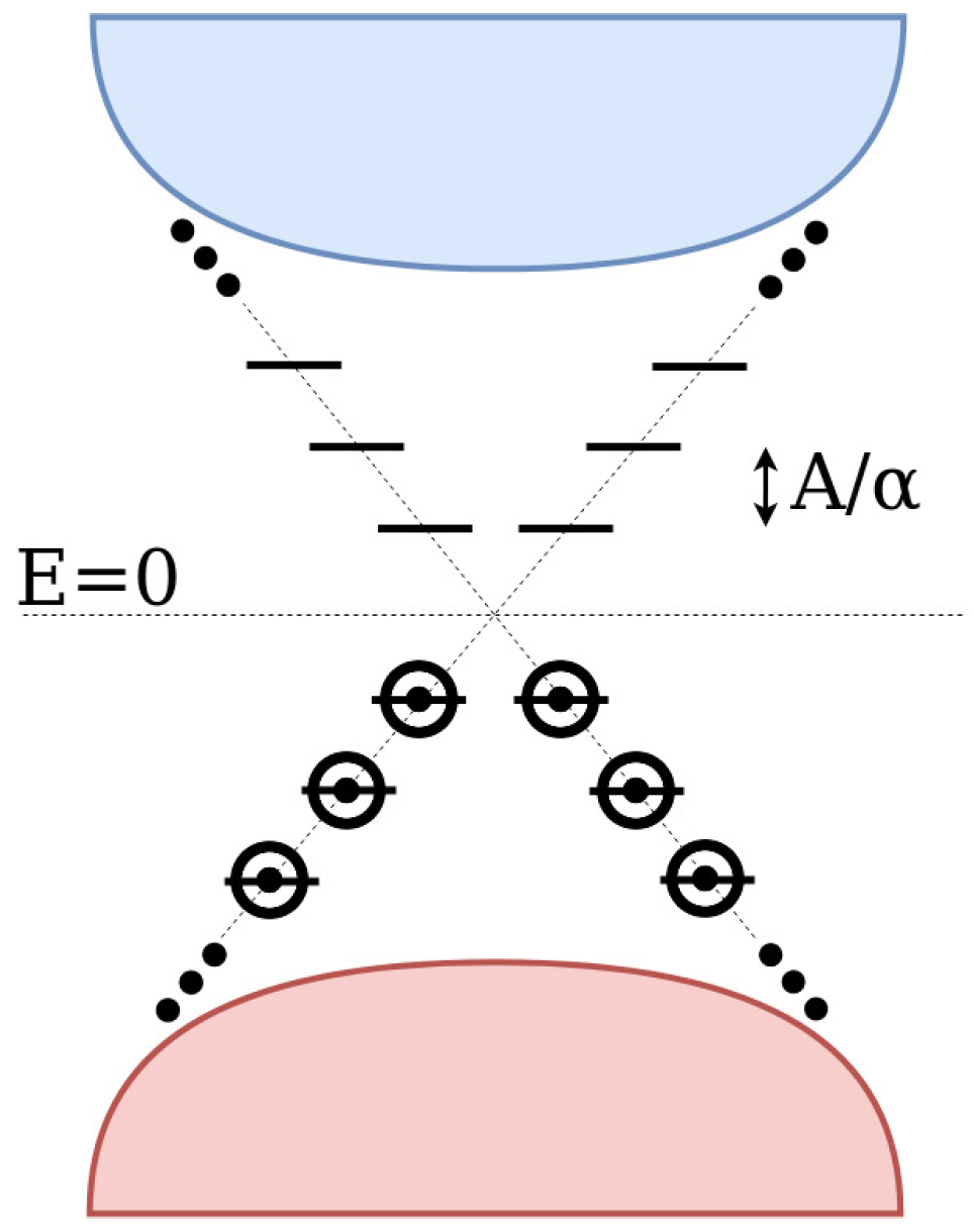
According to this model, the surface states of the nanoparticle become discrete, at energies , ...relative to the Dirac point. Here, eV·Å is a constant obtained from density functional theory calculations [45], while is the radius of the nanoparticle. In Figure 1 we can see a simple diagram depicting these discrete surface states, when only states below the Dirac point are occupied. This is the case that will be presented in Section 4.
Similarly to [41], the bulk dielectric function model we employ is of a simple Lorentzian form
This model includes the contributions from three different excitations in the bulk material: and transverse phonons as well as free carriers f due to defects in the crystal structure.
As shown in the same paper using perturbation theory, the absorption cross section of a nanoparticle in the quasi-static limit is given by
where the term appears because of the interaction between the surface states and the external field. In the special case where we consider the Fermi level below the Dirac point (), this term is given by
It is important to note here that the expression of is only valid for sufficiently weak electric fields, a fact which we have taken into account for our numerical calculations. It should also be noted that the applied electric field is assumed to be perpendicular to the c axis of the crystal.
It is also interesting to note that Equation (2) is reminiscent of the classical equation for the absorption cross section of a dielectric sphere. We can thus approximate the dielectric function of the spherical TINP using the simple expression
This approximation is used extensively in the model we used for the calculation of the absorption of the system, as described in Section 3.
2.2. The SToP Mode
In [41], using Equation (2), the absorption cross section of a TINP was calculated, showing a novel excitation which the authors called a SToP mode (surface topological plasmon mode). The peak corresponding to this mode seems to be characterized by a comparatively high absorption rate, as well as a quite narrow bandwidth. This interesting combination of features could potentially make this excitation a good candidate for achieving strong coupling with quantum emitters.
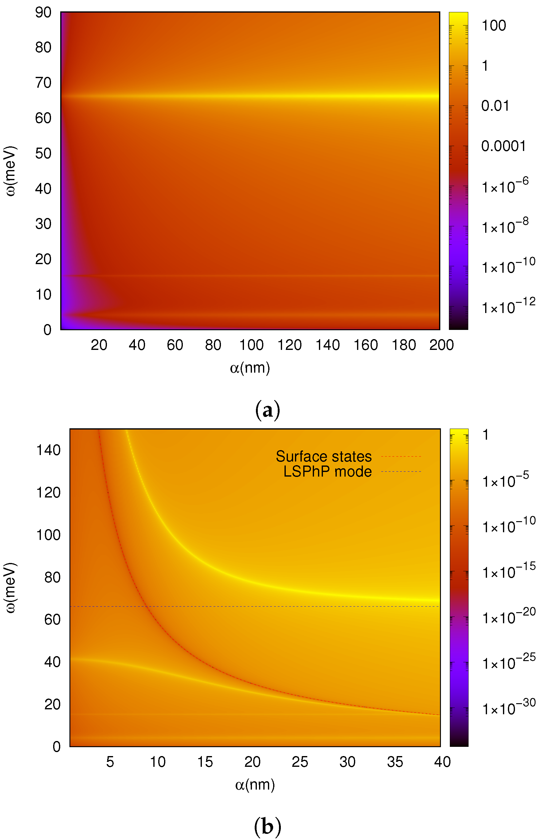
For the sake of completeness, we reproduce the power absorption of the nanoparticle by using Equation (29) (see Section 3), which, for a TINP in a vacuum, yields an equivalent expression to Equation (2) (with the difference of a constant factor): . In Figure 2 we can see the excitations of the TINP for varying values of its radius. Comparing with the case where we ignore the effect of the surface states (a), we can clearly see that including them (b) gives rise to an additional excitation, the SToP mode. The proposed mechanism for the appearance of the SToP mode in [41] is that the surface states act as mediators of the interaction between light and the phonon, which normally does not absorb. The second graph suggests that for relatively small TINP radii, the localized surface phonon polariton (LSPhP) couples strongly to the SToP mode, resulting in splitting behaviour.
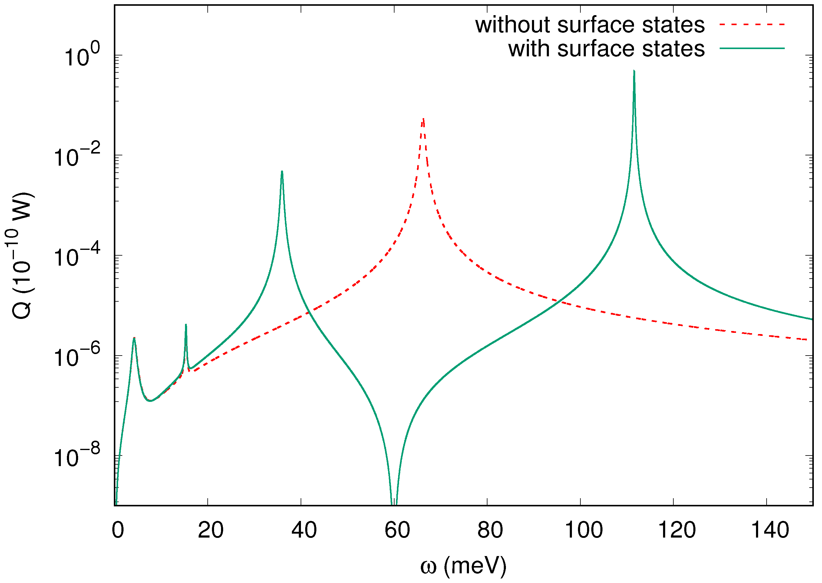
In Figure 3, the SToP mode, along with the other excitations of the TINP, are shown for a nanoparticle with a radius of 10 nm. When we ignore the effects of the surface states (red graph), we see the same three excitations that are also visible in Figure 2a, namely, from left to right: the LSPP, the phonon and the LSPhP. However, when the surface states are taken into account (green graph), a new peak emerges, the SToP. It is exactly this case that we present in more detail in Section 4.
A short note should be made here on how we have determined the nature of these excitations. By comparing the positions of the peaks with the values of the dielectric function, we can conclude that while the phonon peak is a simple resonance, the SToP mode, the LSPP and the LSPhP all occur approximately when and is relatively small, suggesting that these excitations are Fröhlich-type resonances. This hints at the SToP mode being a plasmonic mode, a collective electromagnetic excitation occuring near the surface of the nanoparticle. Another indication for this is the association with free carriers, namely the electrons in the surface states, analogously to the case of the LSPP with the free carriers in the bulk (see Equation (1)).
At this point, we should also note why we have chosen to present this particular case of nanoparticle radius in this work. Firstly, it seems that around this nanoparticle radius there is a significant interaction between the surface states and the LSPhP (see Figure 3). Furthermore, comparisons with tight-binding calculations presented in [41] suggest that this nanoparticle radius could be a suitable lowest bound for the validity of this model. This bound is also interesting as the energy level spacing increases with decreasing radius, and a greater spacing could potentially mean that the topological states are more robust to thermal (scattering) effects at finite temperatures (see also discussion in [41]). Considering all of the above, this lowest bound appears to be a very interesting case to present in this article.
3. Interacting TINP-QE
To investigate whether there exists a strong coupling regime for a TINP-SQD dimer, we derive a formula for the absorption of the dimer. Then, by calculating the corresponding absorption spectra, the presence of splittings or avoided-crossing areas imply the occurence of strong coupling between excitations of the nanoparticles. This section includes a short presentation of the model and the expressions describing the absorption of the interacting QE-TINP system. The interaction between a two level quantum emitter and a classical nanoparticle is theoretically studied in the manner of [46].
3.1. The Model
We consider a spherical TINP of radius , interacting with a semiconductor quantum dot, with the two nanoparticles separated by a distance R. We also assume the two nanoparticles are placed in a matrix with dielectric constant and the system is subjected to an external polarized field of the form .
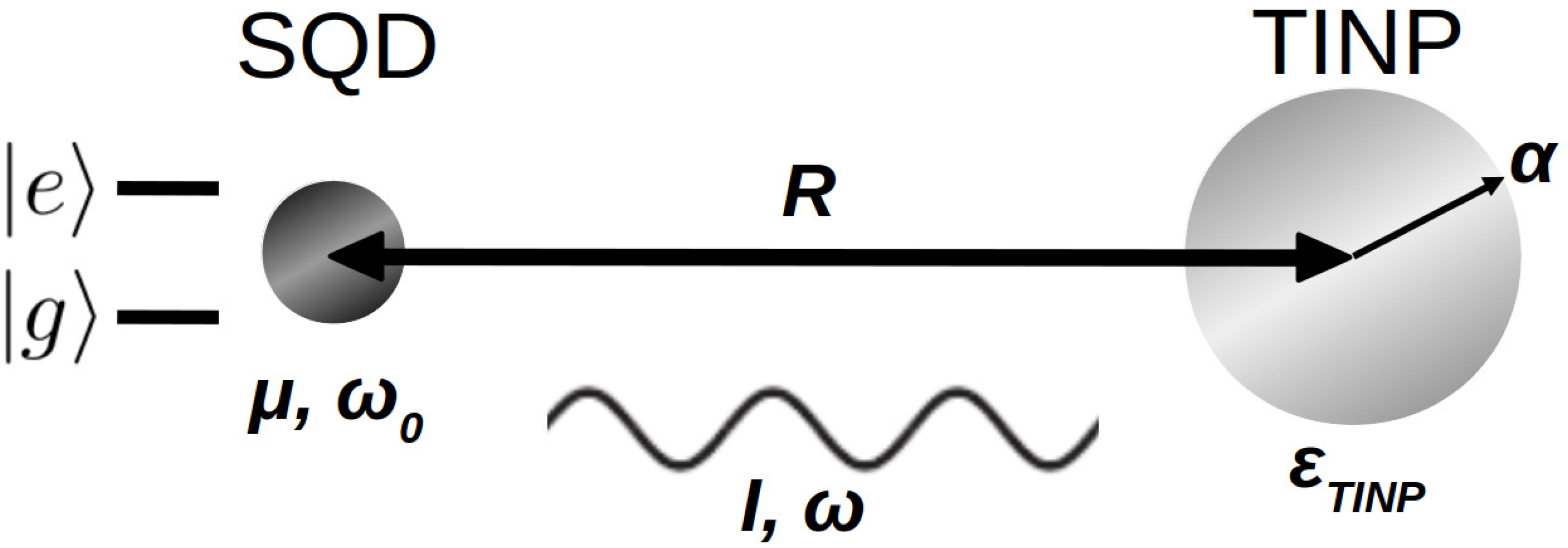
We further assume that the quantum emitter can be described as a simple two-level system with transition energy , transition dipole moment and dielectric constant . We will treat the quantum dot quantum mechanically using a density matrix approach, while we will consider the TINP as a classical spherical particle, described by a dielectric function . The calculation setup is shown in Figure 4.
3.2. Dipole Approximation
We use the following Lindbladian master equation to model the time evolution of the states of the quantum emitter [47,48]:
In this expression, models the relaxation rates of the states, while is the density matrix of the system at a state of equilibrium. It should be noted that acts on the element of , and we assume that for , while for , where are the characteristic relaxation times of the density matrix. More specifically, in this model, is a depopulation (decay) time affecting the diagonal elements and a dephasing time affecting the off-diagonal elements of the density matrix.
The Hamiltonian of the two level system in the dipole approximation is written as
The electric field on the quantum emitter, , can be written as the sum of the externally applied field and the field induced on the emitter by the TINP
where is the effective permittivity of the SQD (see [49]) and when the applied field is parallel (perpendicular) to the major axis of the system. The polarization of the TINP, , will then be given by the Hermitian expression
where (see [49]) and are the positive and negative frequency parts of the electric field on the TINP. In turn, the electric field on the TINP, , will be given as the sum of the external plus the induced field from the SQD
The polarization of the SQD can then be found by using the non-diagonal elements of its density matrix [48]
Factoring out the high-frequency time dependence of the off-diagonal terms of the density matrix we get
Substituting into and then subsequently into , we can use the resulting expression to find in terms of and
where we have defined the quantities (as in [46])
3.3. Interaction Picture and Rotating Wave Approximation
Before we apply the rotating wave approximation, we will first transform the Hamiltonian to the interaction picture. We thus write the Hamiltonian in the form
where is the unperturbed Hamiltonian of the two-level system while describes the perturbation due to the external field as well as the induced field from the TINP. To change the Hamiltonian to the interaction picture we apply the unitary transformation
Now, we need to apply an appropriate transformation to the master equation in order to make use of the transformed Hamiltonian. The most obvious method would be by applying the same transformation
It can easily be shown that the transformed master equation can be rewritten in the simpler form
where and .
If we choose the representation and , then it can easily be shown that the first term is
while the last term in the master equation becomes
The Hamiltonian in the interaction picture is
It is easy to see that , whereas the second term is non-trivial
Therefore we have
and substituting for the expression of and by applying the RWA, we finally find that
3.4. Time Evolution of the QE States
Now we can substitute the expressions we have calculated above into our transformed master equation
eventually giving us a set of four coupled differential equations:
If we define , and then we can find three coupled differential equations for and :
The solutions of these coupled equations will be used to calculate the absorption rate of the system, as described in the following section.
3.5. Absorption of the System
For the absorption of the system, we assume that we can write the total absorption as the sum of two components: one contributed by the quantum emitter and one by contributed by the TINP, i.e.,
For the quantum emitter, the absorption can be calculated using the simple expression
which of course can be written in terms of
For the TINP, we can use
where j is the current density, whereas is the electric field inside the nanoparticle.
By substituting Equation (9) in Equation (8) and by using Equation (10) with , we can write the field in the TINP in the form , where
The electric field inside the TINP can then be written in the convenient form
with being the effective dielectric function of the TINP.
For the current density, we use , where V is the volume of the spherical nanoparticle. Using in Equation (7), we can write
By calculating j and substituting in the expression for , Equation (29), we can eventually get the expression
To summarize, we have found the steady-state solution of the density matrix, expressed through the quantities and . Using these steady-state values, we can then calculate the absorption rates of the SQD and TINP, respectively.
4. Numerical Results and Discussion
In the previous sections, we have presented an overview of the excitations of a TINP of radius nm (Section 2.2), as well as of the model we have employed for the interacting TINP-quantum emitter system (Section 3). In this section, after first presenting our choice of parameters and giving a brief description of our methodology in studying the system, we show how the interaction between the SToP mode of the TINP and the exciton of the QE gives rise to a topological plexciton.
4.1. Problem Parameters
We assume a spherical TINP of radius nm, modeled by the dielectric function described in Section 2.1. We include the effect of the surface states in the response of the nanoparticle, expressed through the perturbation term , which, assuming the Fermi level is below the Dirac point, is given by Equation (3).
We assume that the quantum emitter has a constant dielectric function and that its dipole moment is e·nm, though we allow its value to vary in some cases in order to show its effect on the splitting. For the relaxation times we have assumed a linear dependence on the transition frequency: ns eV, ns eV, where is the exciton transition frequency and 0.8 ns, 0.3 ns the relaxation times at eV. All these correspond to typical values for CdSe-based quantum dots [46,50,51,52,53,54]. For the SToP mode at a TINP radius nm (≈36 meV), this provides relaxation times on the order of ( ps, ps). Comparing with [55], concerning lifetimes of SQD intersublevel transitions in the terahertz range, this seems to be a decent (and maybe a quite conservative) approximation. Lastly, for the initial conditions of the density matrix we have taken , which is a simple mixed state of the ground and excited states of the quantum emitter.
As for the other parameters, the separation distance R could, in principle, take any value greater than the sum of the radii of the two nanoparticles. In our study, however, we used the radius of the TINP as the lowest limit to the separation, to identify the limits of the splitting when the emitter is of a very small (negligible) size. We have assumed a field intensity W/cm2, with the electric field applied along the main axis of the system (so ). For the background material we have assumed that .
4.2. Method of Study
In our previous analysis of Section 3, we have applied the dipole and rotating-wave approximations to derive equations to describe our system. Therefore, for any choice of , we only study the absorption spectrum for exciting field energies around this value. For this system, we generally choose close to the SToP peak for a TINP of radius nm, which is around ≈36 meV.
4.3. Strong Coupling between the SToP Mode and the Exciton
Next, we study the conditions under which strong coupling occurs between the SToP mode of the TINP and the exciton of the SQD. More specifically, we observe splitting behaviour, which suggests operation in the strong coupling regime and the creation of a novel hybrid excitation, a (localized) surface topological plexciton.
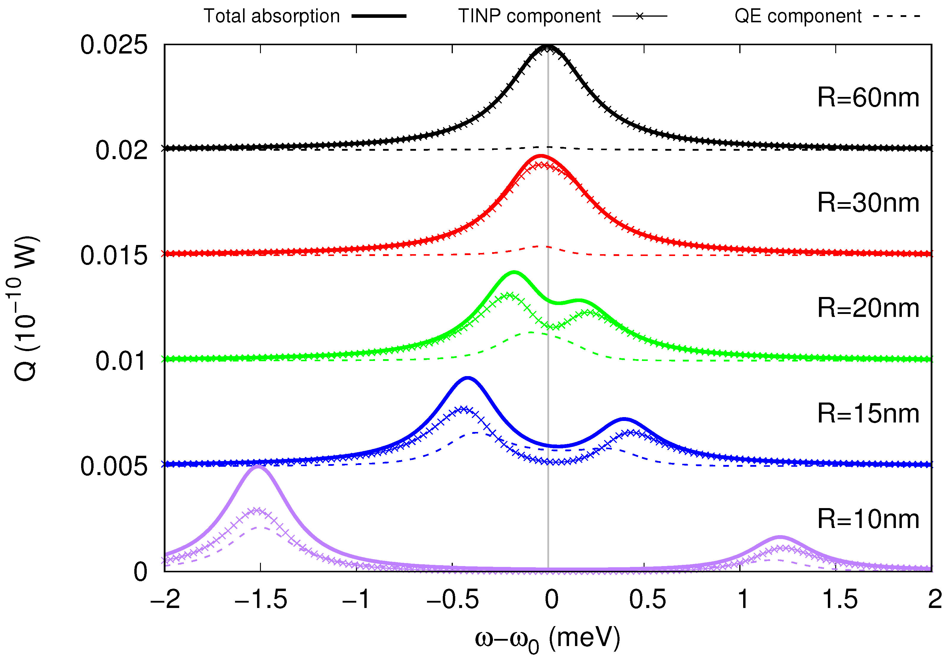
In Figure 5 we see the effect of decreasing the separation distance between the nanoparticles. Here, we assume e·nm and exciton transition frequency close to the SToP mode. On each graph, the components contributed by each nanoparticle are also visible. It is clear that the splitting increases with decreasing distance, reaching a maximum of ≈2.75 meV at the limiting case nm. The strong coupling is also evident from the fact that the splitting is visible in both components of the absorption.
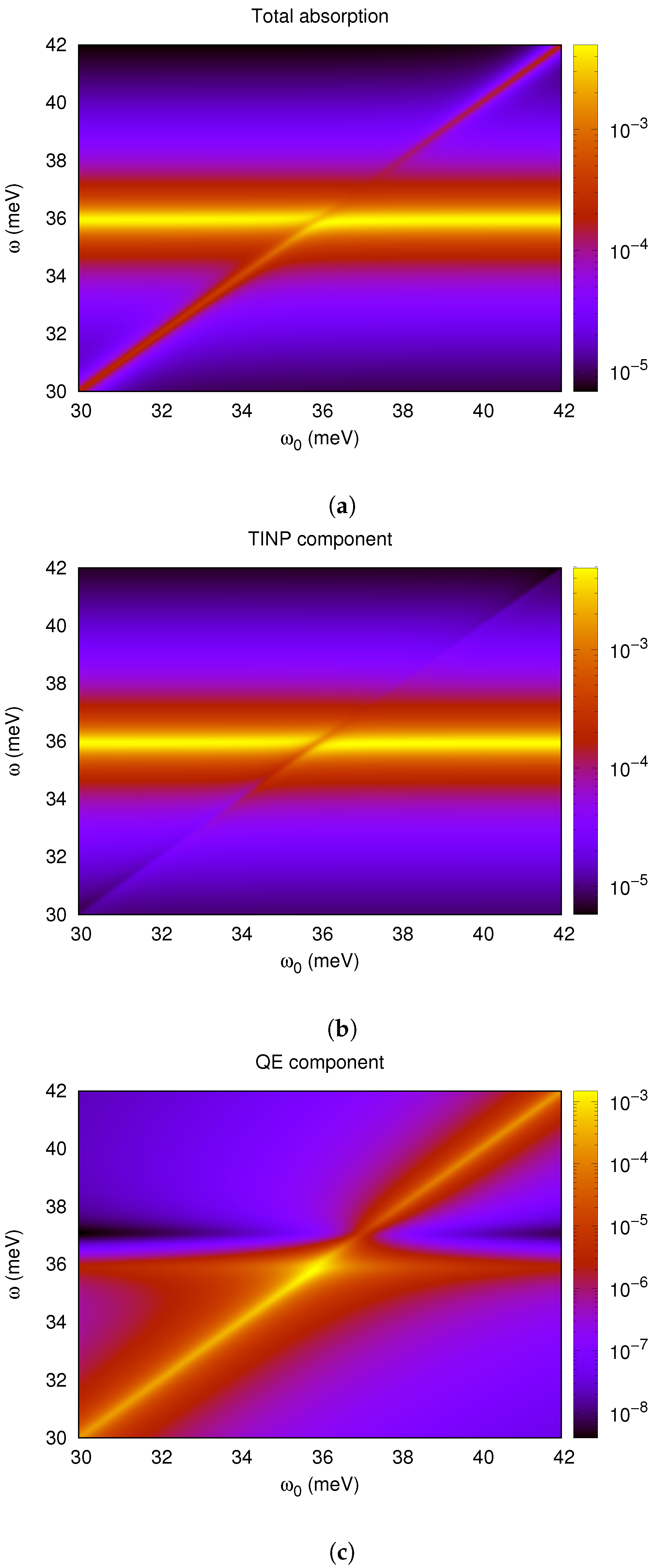
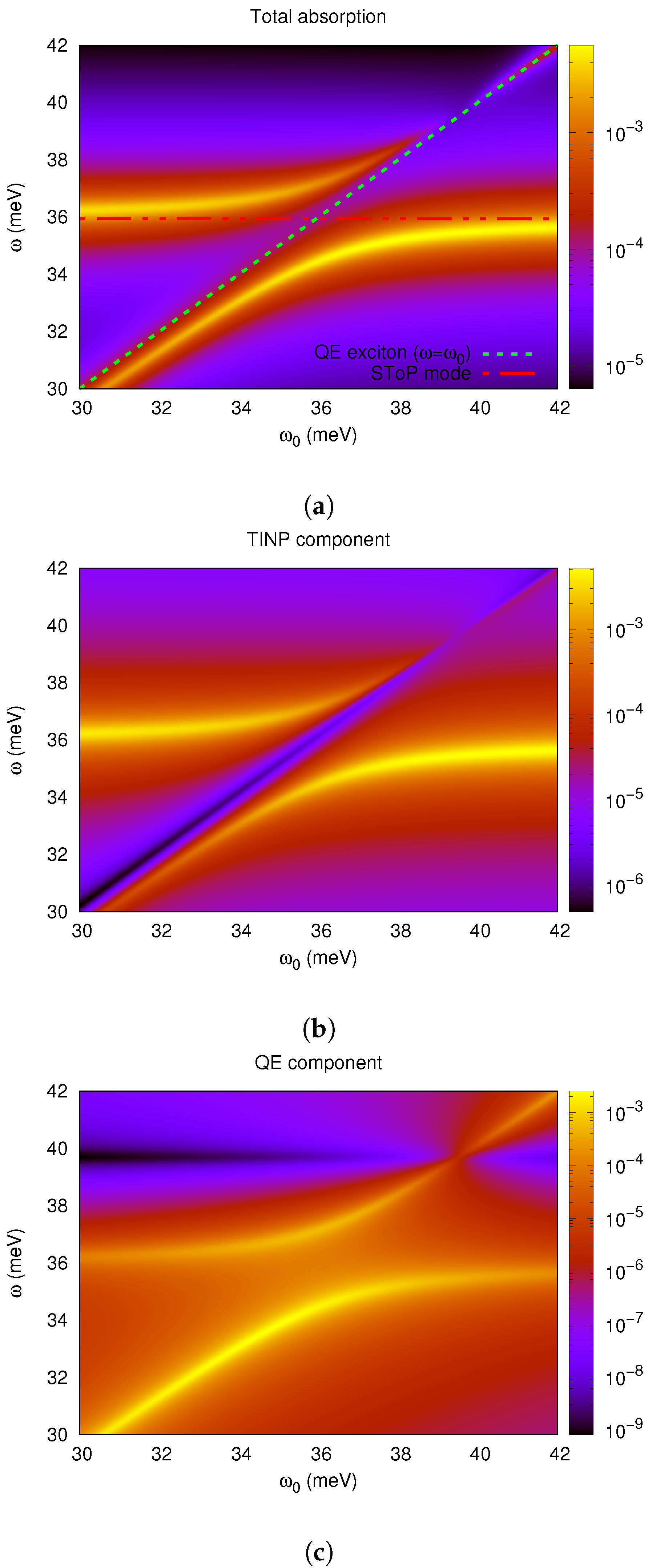
In Figure 6 and Figure 7 we see the splitting when we vary the transition frequency of the quantum emitter for specific values of R and . In the same figures, other than the total absorption of the system (top graph), we can also see the components contributed by the TINP (bottom left) and by the quantum emitter (bottom right). Two cases are presented: in Figure 6, for nm, and in Figure 7 for nm, for the same value of the dipole moment e·nm. By comparing the two figures, we can see that once again the same trend is visible. Namely, when we decrease the separation distance, we observe a marked increase in the splitting, and thus in the coupling between the two excitations. As in the previous case, we also identify the same splitting behaviour appearing in both components of the absorption, implying the increased coherence of the state.
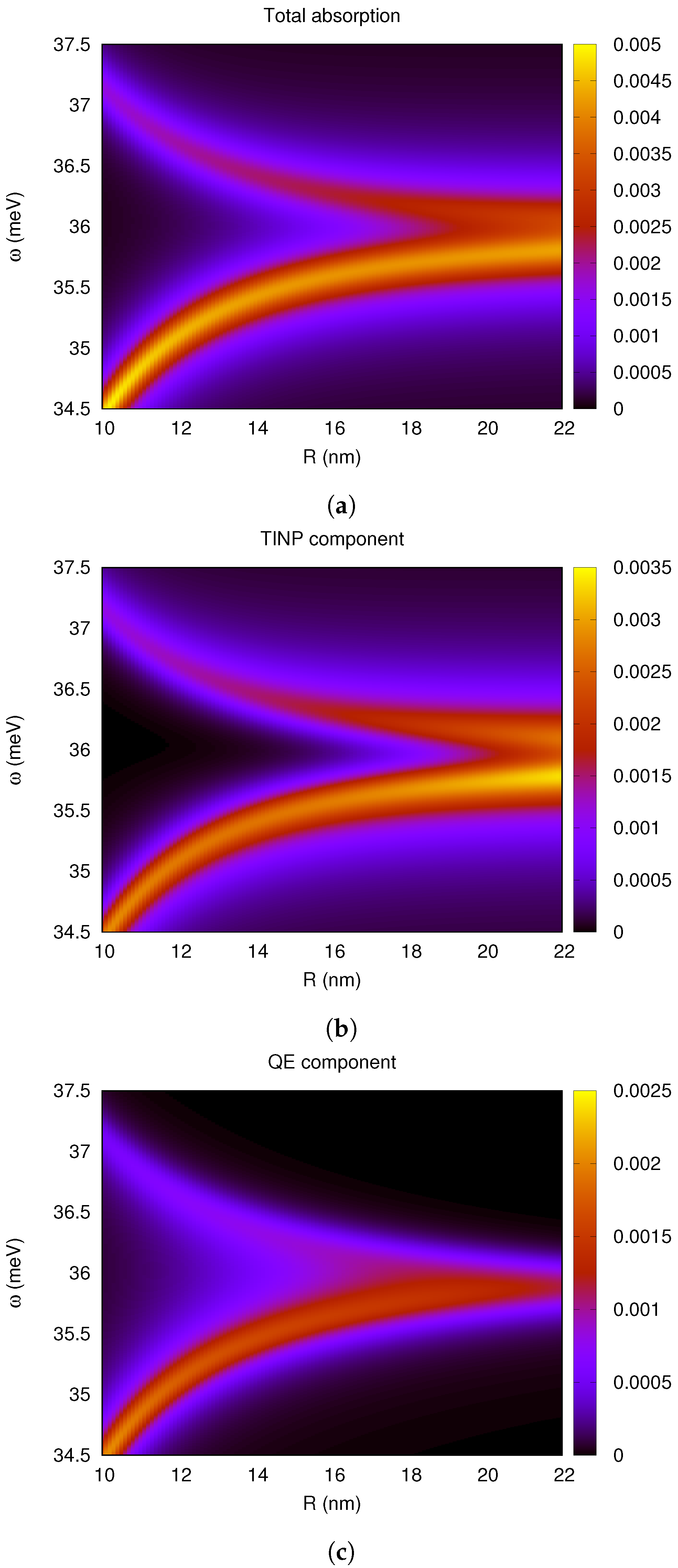
The results when varying with constant R follow the inverse trend of varying R with constant , i.e., the splitting increases by increasing the dipole moment . Both of these trends can also be summarized by the graphs in Figure 8 and Figure 9. In Figure 8, we concisely see the effect of varying the separation distance R with constant e·nm. We can see that the splitting in the total absorption emerges at values around 20 nm, while it becomes visible in both components at values below 16 nm. These graphs suggest a maximum splitting of about 2 meV at the limiting case nm.
In Figure 9, we see the effect of varying with nm. In this case, we see that the splitting emerges for quite small values of the dipole moment, apparently around e·nm. These graphs suggest a splitting of almost 3 meV at e·nm for the limiting case of touching nanoparticles. If we use a value of 2 meV as indicative of the possible size of the coupling and compare it with the exciton transition frequency, we obtain the ratio: meV/36 meV , which should place the system well within the strong coupling regime according to common classification schemes [56,57].
4.4. Outlook
At this point, it might be conducive to highlight a few limitations of the model and indicate a few possibilities for future research. A first thing to notice is the perturbative approach in modeling the dielectric function, preventing us from studying the system beyond the weak-field limit. Therefore, developing a non-perturbative approach could allow for a richer exploration of the interaction. Another thing to consider would be working outside the dipole and rotating-wave approximations, or even attempting a fully quantum treatment of the problem, in order to obtain a fuller and more accurate description.
Moreover, an important assumption that was made in this model was that the system operates at a very low temperature, allowing us to largely ignore phonon interactions in the nanoparticles and from any surrounding medium. At higher temperatures, however, we would likely need to somehow take these effects into account. However this is not crucial for the study presented here since recent theoretical work [43] seems to support the symmetry protection of the surface states in TINPs, which is expected to limit phonon interactions by preventing backscattering. Moreover, recent experiments at room temperature [58] have pointed out that the low-temperature effects discussed here can realistically persist at higher temperatures.
In terms of applications, these results may be useful for the exploration of novel, exotic phases of matter or to further research in the area of topological insulator plasmonics, but also for applications in the far-infrared and quantum computing. For example, we could think of sensing applications in the far infrared by studying the effect of the surrounding or adjacent material or the influence of the separation distance on the properties of the system. We could also consider using ensembles of QEs and/or ensembles of TINPs instead of a simple nanoparticle dimer. One possible example would be an implementation of a “spaser” making use of the SToP mode in the TINP and using a set of surrounding quantum emitters as the active medium [59].
It might also be interesting to consider placing similar systems in (narrow linewidth) optical resonators, for example to possibly suppress interactions with phonons in the nanoparticles and in the surrounding medium [60,61]. As was noted in [41], this system could be of interest in quantum information applications because of the ability to adjust the Fermi level of the TINP and the different response of the surface states to circularly and linearly polarized light. Since the topological nature of the surface states [43] has been experimentally demonstrated for TINPs [58], the discretized states of the TINP could then be used as basis states for a qubit that is more resistant to decoherence. Finally, the ability to control and manipulate the strong coupling in the reported system may facilitate the creation and preservation of quantum coherence and entanglement, both crucial aspects in quantum computing.
5. Conclusions
In summary, we report a novel hybrid mode, a surface topological plexciton, arising from strong coupling between the exciton of a two-level quantum emitter and the surface topological plasmon (SToP) mode of a topological insulator nanoparticle (TINP) [41]. Our results suggest that the plexcitonic modes may exhibit a vacuum Rabi splitting of at least 2 meV for a TINP with a radius of 10 nm (SToP mode ∼36 meV) and a quantum emitter with dipole moment e·nm, which corresponds to a ratio meV/36 meV , suggesting that our system is operating in the strong coupling regime. The presence of strong coupling in this novel system may open up new possibilities for exploring exotic phases of matter and plasmonics in topological insulators, as well as for applications in the far-infrared technology and in quantum computing.
Author Contributions
Methodology, G.K. and V.Y.; validation, V.Y.; investigation, G.K. and V.Y.; resources, G.K. and V.Y.; data curation, G.K.; writing—original draft preparation, G.K.; writing—review and editing, G.K. and V.Y.; visualization, G.K.; supervision, V.Y. All authors have read and agreed to the published version of the manuscript.
Funding
The Center for Polariton-driven Light–Matter Interactions (POLIMA) is sponsored by the Danish National Research Foundation (Project No. DNRF165).
Institutional Review Board Statement
Not applicable.
Informed Consent Statement
Not applicable.
Data Availability Statement
The data presented in this study are available on reasonable request from the corresponding author.
Conflicts of Interest
The authors declare no conflict of interest.
References
- Dovzhenko, D.S.; Ryabchuk, S.V.; Rakovich, Y.P.; Nabiev, I.R. Light–matter interaction in the strong coupling regime: Configurations, conditions and applications. Nanoscale 2018, 10, 3589–3605. [Google Scholar] [CrossRef]
- Yu, X.; Yuan, Y.; Xu, J.; Yong, K.; Qu, J.; Song, J. Strong Coupling in Microcavity Structures: Principle, Design, and Practical Application. Laser Photonics Rev. 2019, 13, 1800219. [Google Scholar] [CrossRef]
- Rice, P.R.; Carmichael, H.J. Photon statistics of a cavity-QED laser: A comment on the laser–phase-transition analogy. Phys. Rev. A 1994, 50, 4318–4329. [Google Scholar] [CrossRef]
- Hertzog, M.; Wang, M.; Mony, J.; Börjesson, K. Strong light–matter interactions: A new direction within chemistry. Chem. Soc. Rev. 2019, 48, 937–961. [Google Scholar] [CrossRef]
- Maier, S.A. Plasmonics: Fundamentals and Applications; Springer: Berlin/Heidelberg, Germany, 2007. [Google Scholar]
- Yu, H.; Peng, Y.; Yang, Y.; Li, Z.Y. Plasmon-enhanced light–matter interactions and applications. NPJ Comput. Mater. 2019, 5, 45. [Google Scholar] [CrossRef]
- Stockman, M.I.; Kneipp, K.; Bozhevolnyi, S.I.; Saha, S.; Dutta, A.; Ndukaife, J.; Kling, M.F. Roadmap on plasmonics. IOP J. Opt. 2018, 20, 043001. [Google Scholar] [CrossRef]
- Atwater, H.A. The Promise of Plasmonics. Sci. Am. Spec. Ed. 2007, 17, 56–63. [Google Scholar] [CrossRef]
- Verma, S.S. Plasmonics in Nanomedicine: A Review. Glob. J. Nanomed. 2018, 4, 2573–2574. [Google Scholar] [CrossRef]
- Tame, M.S.; McEnery, K.R.; Özdemir, S.K.; Lee, J.; Maier, S.A.; Kim, M.S. Quantum Plasmonics. Nat. Phys. 2013, 9, 329–340. [Google Scholar] [CrossRef]
- Törmä, P.; Barnes, W.L. Strong Coupling between surface plasmon polaritons and emitters: A review. Rep. Prog. Phys. 2015, 78, 013901. [Google Scholar] [CrossRef]
- Bellessa, J.; Bonnand, C.; Plenet, J.C.; Mugnier, J. Strong Coupling between Surface Plasmons and Excitons in an Organic Semiconductor. Phys. Rev. Lett. 2004, 93, 036404. [Google Scholar] [CrossRef]
- Dintinger, J.; Klein, S.; Bustos, F.; Barnes, W.L.; Ebbesen, T.W. Strong coupling between surface plasmon-polaritons and organic molecules in subwavelength hole arrays. Phys. Rev. B 2005, 71, 035424. [Google Scholar] [CrossRef]
- Dintinger, J.; Klein, S.; Ebbesen, T.W. Molecule–Surface Plasmon Interactions in Hole Arrays: Enhanced Absorption, Refractive Index Changes, and All-Optical Switching. Adv. Mater. 2006, 18, 1267–1270. [Google Scholar] [CrossRef]
- Sugawara, Y.; Kelf, T.A.; Baumberg, J.J.; Abdelsalam, M.E.; Bartlett, P.N. Strong Coupling between Localized Plasmons and Organic Excitons in Metal Nanovoids. Phys. Rev. Lett. 2006, 97, 266808. [Google Scholar] [CrossRef]
- Wurtz, G.A.; Evans, P.R.; Hendren, W.; Atkinson, R.; Dickson, W.; Pollard, R.J.; Zayats, A.V.; Harrison, W.; Bower, C. Molecular Plasmonics with Tunable Exciton–Plasmon Coupling Strength in J-Aggregate Hybridized Au Nanorod Assemblies. Nano Lett. 2007, 7, 1297–1303. [Google Scholar] [CrossRef]
- Chovan, J.; Perakis, I.E.; Ceccarelli, S.; Lidzey, D.G. Controlling the interactions between polaritons and molecular vibrations in strongly coupled organic semiconductor microcavities. Phys. Rev. B 2008, 78, 045320. [Google Scholar] [CrossRef]
- Fofang, N.T.; Park, T.H.; Neumann, O.; Mirin, N.A.; Norlander, P.; Halas, N.J. Plexcitonic Nanoparticles: Plasmon-Exciton Coupling in Nanoshell-J-Aggregate Complexes. Nano Lett. 2008, 8, 3481–3487. [Google Scholar] [CrossRef]
- Bellessa, J.; Symonds, C.; Vynck, K.; Lemaitre, A.; Brioude, A.; Beaur, L.; Valvin, P. Giant Rabi splitting between localized mixed plasmon-exciton states in a two-dimensional array of nanosize metallic disks in an organic semiconductor. Phys. Rev. B 2009, 80, 033303. [Google Scholar] [CrossRef]
- Schlather, A.E.; Large, N.; Urban, A.S.; Nordlander, P.; Halas, N.J. Near-Field Mediated Plexcitonic Coupling and Giant Rabi Splitting in Individual Metallic Dimers. Nano Lett. 2013, 13, 3281–3286. [Google Scholar] [CrossRef] [PubMed]
- Pockrand, I.; Swalen, J.D.; Santo, R.; Brillante, A.; Philpott, M.R. Optical properties of organic dye monolayers by surface plasmon spectroscopy. J. Chem. Phys. 1978, 69, 4001–4011. [Google Scholar] [CrossRef]
- Hakala, T.K.; Toppari, J.J.; Kuzyk, A.; Pettersson, M.; Tikkanen, H.; Kunttu, H.; Törmä, P. Vacuum Rabi Splitting and Strong-Coupling Dynamics for Surface-Plasmon Polaritons and Rhodamine 6G Molecules. Phys. Rev. Lett. 2009, 103, 053602. [Google Scholar] [CrossRef]
- Väkeväinen, A.I.; Moerland, R.J.; Rekola, H.T.; Eskelinen, A.P.; Martikainen, J.P.; Kim, D.H.; Törmä, P. Plasmonic Surface Lattice Resonances at the Strong Coupling Regime. Nano Lett. 2014, 14, 1721–1727. [Google Scholar] [CrossRef]
- Gomez, D.E.; Vernon, K.C.; Mulvaney, P.; Davis, T.J. Surface Plasmon Mediated Strong Exciton–Photon Coupling in Semiconductor Nanocrystals. Nano Lett. 2010, 10, 274–278. [Google Scholar] [CrossRef]
- Gomez, D.E.; Vernon, K.C.; Mulvaney, P.; Davis, T.J. Coherent superposition of exciton states in quantum dots induced by surface plasmons. Appl. Phys. Lett. 2010, 96, 073108. [Google Scholar] [CrossRef]
- Manuel, A.P.; Kirkey, A.; Mahdia, N.; Shankar, K. Plexcitonics–fundamental principles and optoelectronic applications. J. Mater. Chem. C 2019, 7, 1821–1853. [Google Scholar] [CrossRef]
- Yuen-Zhou, J.; Saikin, S.K.; Zhu, T.; Onbasli, M.C.; Ross, C.A.; Bulovic, V.; Baldo, M.A. Plexciton Dirac points and topological modes. Nat. Commun. 2016, 7, 11783. [Google Scholar] [CrossRef] [PubMed]
- Politano, A.; Viti, L.; Vitiello, M.S. Optoelectronic devices, plasmonics and photonics with topological insulators. APL Mater. 2017, 5, 035504. [Google Scholar] [CrossRef]
- Hasan, M.Z.; Kane, C.L. Topological Insulators. Rev. Mod. Phys 2010, 82, 3045. [Google Scholar] [CrossRef]
- Bernevig, B.A.; Hughes, T.L. Topological Insulators and Topological Superconductors; Princeton University Press: Princeton, NI, USA, 2013. [Google Scholar]
- Moore, J.E. The Birth of Topological Insulators. Nature 2010, 464, 194–198. [Google Scholar] [CrossRef]
- Qi, X.; Zhang, S. Topological Insulators and Superconductors. Rev. Mod. Phys. 2011, 83, 1057–1110. [Google Scholar] [CrossRef]
- West, P.R.; Ishii, S.; Naik, G.V.; Emani, N.K.; Shalaev, V.M.; Boltasseva, A. Searching for better plasmonic materials. Laser Photon. Rev. 2010, 4, 795–808. [Google Scholar] [CrossRef]
- Jongbum, K.; Gururaj, N.; Naresh, E.; Urcan, G.; Alexandra, B. Plasmonic Resonances in Nanostructured Transparent Conducting Oxide Films. Sel. Top. Quantum Electron. IEEE J. 2013, 19, 4601907. [Google Scholar] [CrossRef]
- Naik, G.V.; Schroeder, J.L.; Ni, X.; Kildishev, A.V.; Sands, T.D.; Boltasseva, A. Titanium nitride as a plasmonic material for visible and near-infrared wavelengths. Opt. Mater. Express 2012, 2, 478–479. [Google Scholar] [CrossRef]
- Luo, X.; Qiu, T.; Lu, W.; Ni, Z. Plasmons in graphene: Recent progress and applications. Mater. Sci. Eng. R Rep. 2013, 74, 351–376. [Google Scholar] [CrossRef]
- Karch, A. Surface Plasmons and Topological Insulators. Phys. Rev. B Condens. Matter 2011, 83, 245432. [Google Scholar] [CrossRef]
- Stauber, T.; Gómez-Santos, O.G.; Brey, L. Plasmonics in topological insulators: Spin-charge separation, the influence of the inversion layer, and phonon-plasmon coupling. ACS Photonics 2017, 4, 2978–2988. [Google Scholar] [CrossRef]
- Pietro, P.D.; Ortolani, M.; Limaj, O.; Gaspare, A.D.; Giliberti, V.; Giorgianni, F.; Brahlek, M.; Bansal, N.; Koirala, N.; Oh, S.; et al. Observation of Dirac plasmons in a topological insulator. Nat. Nanotechnol. 2013, 8, 556–560. [Google Scholar] [CrossRef]
- Jiang, Z.; Rösner, M.; Groenewald, R.E.; Haas, S. Localized Plasmons in Topological Insulators. arXiv 2019, arXiv:1907.12432v2. [Google Scholar] [CrossRef]
- Siroki, G.; Lee, D.K.K.; Haynes, P.D.; Giannini, V. Single-electron induced surface plasmons on a topological nanoparticle. Nat. Commun. 2016, 7, 12375. [Google Scholar] [CrossRef]
- Xia, Y.; Qian, D.; Hsieh, D.; Wray, L.; Pal, A.; Lin, H.; Bansil, A.; Grauer, D.; Hor, Y.S.; Cava, R.J.; et al. Observation of a large-gap topological-insulator class with a single Dirac cone on the surface. Phys. Rev. Lett. 2009, 5, 398–402. [Google Scholar] [CrossRef]
- Gleb, S.; Haynes, P.D.; Lee, D.K.; Vincenzo, G. Protection of surface states in topological nanoparticles. Phys. Rev. Mat. 2017, 1, 024201. [Google Scholar] [CrossRef]
- Imura, K.; Yoshimura, Y.; Takane, Y.; Fukui, T. Spherical topological insulator. Phys. Rev. B 2012, 86, 235119. [Google Scholar] [CrossRef]
- Liu, C.; Qi, X.; Zhang, H.; Dai, X.; Fang, Z.; Zhang, S. Model Hamiltonian for topological insulators. Phys. Rev. B 2010, 82, 045122. [Google Scholar] [CrossRef]
- Artuso, R.D.; Bryant, G.W. Strongly coupled quantum dot-metal nanoparticle systems: Exciton-induced transparency, discontinuous response, and suppression as driven quantum oscillator effects. Phys. Rev. B 2010, 82, 195419. [Google Scholar] [CrossRef]
- Karplus, R.; Schwinger, J. A Note on Saturation in Microwave Spectroscopy. Phys. Rev. 1948, 73, 1020. [Google Scholar] [CrossRef]
- Yariv, A. Quantum Electronics, Appendix 4: Quantum Mechanical Derivation of Nonlinear Optical Constants; John Wiley & Sons: Hoboken, NJ, USA, 1989. [Google Scholar]
- Bohren, C.F.; Huffman, D.R. Absorption and Scattering of Light by Small Particles, Chapter 5: Particles Small Compared with the Wavelength, Section 5.2: The Electrostatics Approximation; John Wiley & Sons: Hoboken, NJ, USA, 1983. [Google Scholar]
- Zhang, W.; Govorov, A.O.; Bryant, G.W. Semiconductor-Metal Nanoparticle Molecules: Hybrid Excitons and the Nonlinear Fano Effect. Phys. Rev. Lett. 2006, 97, 146804. [Google Scholar] [CrossRef] [PubMed]
- Yan, J.Y.; Zhang, W.; Duan, S.Q.; Zhao, X.G.; Govorov, A.O. Optical properties of coupled metal-semiconductor and metal-molecule nanocrystal complexes: Role of multipole effects. Phys. Rev. B 2008, 77, 165301. [Google Scholar] [CrossRef]
- Artuso, R.D.; Bryant, G.W. Optical Response of Strongly Coupled Quantum Dot-Metal Nanoparticle Systems: Double Peaked Fano Structure and Bistability. Nano Lett. 2008, 8, 2106–2111. [Google Scholar] [CrossRef]
- Paspalakis, E.; Evangelou, S.; Terzis, A.F. Control of excitonic population inversion in a coupled semiconductor quantum dot–metal nanoparticle system. Phys. Rev. B 2013, 87, 235302. [Google Scholar] [CrossRef]
- Yang, W.; Chen, A.; Huang, Z.; Lee, R. Ultrafast optical switching in quantum dot-metallic nanoparticle hybrid systems. Opt. Express 2015, 23, 13032–13040. [Google Scholar] [CrossRef]
- Zibik, E.A.; Grange, T.; Carpenter, B.A.; Porter, N.E.; Ferreira, R.; Bastard, G.; Stehr, D.; Winnerl, S.; Helm, M.; Liu, H.Y.; et al. Long lifetimes of quantum-dot intersublevel transitions in the terahertz range. Nat. Mater. Lett. 2009, 8, 803–807. [Google Scholar] [CrossRef]
- Moroz, A. A hidden analytic structure of the Rabi model. Ann. Phys. 2014, 340, 252–266. [Google Scholar] [CrossRef]
- Kockum, A.F.; Miranowicz, A.; Liberato, S.D.; Savasta, S.; Nori, F. Ultrastrong coupling between light and matter. Nat. Rev. Phys. 2019, 1, 19–40. [Google Scholar] [CrossRef]
- Rider, M.S.; Sokolikova, M.; Hanham, S.M.; Navarro-Cia, M.; Haynes, P.D.; Lee, D.K.K.; Daniele, M.; Guidi, M.C.; Mattevi, C.; Lupi, S.; et al. Experimental signature of a topological quantum dot. Nanoscale 2020, 12, 22817–22825. [Google Scholar] [CrossRef]
- Bergman, D.J.; Stockman, I.M. Surface Plasmon Amplification by Stimulated Emission of Radiation: Quantum Generation of Coherent Surface Plasmons in Nanosystems. Phys. Rev. Lett. 2003, 90, 027402. [Google Scholar] [CrossRef]
- Denning, E.V.; Iles-Smith, J.; Gregersen, N.; Mork, J. Phonon effects in quantum dot single-photon sources. Opt. Mater. Express 2020, 10, 222–239. [Google Scholar] [CrossRef]
- Denning, E.V.; Iles-Smith, J.; Mork, J. Quantum light-matter interaction and controlled phonon scattering in a photonic Fano cavity. Phys. Rev. B 2019, 100, 214306. [Google Scholar] [CrossRef]
Figure 1.
The discrete energy levels of a nanoparticle subjected to light [41]. Here we assume that only energy levels below the Dirac point are occupied.
Figure 1.
The discrete energy levels of a nanoparticle subjected to light [41]. Here we assume that only energy levels below the Dirac point are occupied.

Figure 2.
The excitations of the nanoparticle: Power absorption heatmap ( W) as a function of the exciting energy (meV) (vertical axis) and the nanoparticle radius (nm) (horizontal axis). (a) Excitations of the TINP when we ignore the effect of the surface states. From top to bottom, the visible excitations are: the localized surface phonon polariton (LSPhP), the phonon and the LSPP. (b) Excitations of the TINP when we include the surface states. Here, we focus on radii below 40 nm, where the interaction between the LSPhP (blue line) and the surface states (red line) is clearly visible. We can now see an additional excitation, the SToP mode, located between the LSPhP and the phonon.

Figure 3.
The excitations of a 10 nm nanoparticle. Red dotted line: Excitations of the TINP when we ignore the surface states. Only three excitations are visible in this case (left to right): LSPP, phonon and a localized surface phonon polariton. Green continuous line: Excitations of the TINP when we include the effect of the surface states. In this case we see an additional excitation, the SToP mode. In particular we can see (from left to right): LSPP, phonon, SToP mode and the localized surface phonon polariton.

Figure 4.
Our system consists of an interacting topological insulator nanoparticle (TINP) made of and a two-level quantum emitter (QE, here denoted SQD, for semiconductor quantum dot), and the system is irradiated by a harmonic exciting field of intensity I and frequency . The TINP has a radius and is described by a permittivity , while the QE is described by a transition dipole moment and a transition frequency .

Figure 5.
From weak to strong coupling: emergence of splitting as we vary the separation distance R. The figure shows the power absorption spectrum Q ( W) for decreasing values of R (nm), for a constant emitter dipole moment e·nm. The horizontal axis is the difference between the exciting frequency and the QE transition frequency , with meV in order to match the spectral position of the SToP mode. On each graph the absorption components contributed by the quantum emitter (smooth line) and the TINP (textured line) are also visible below the total absorption line, allowing us to observe that the splitting also appears in the absorption components of the system. These results suggest that for a sufficiently small separation of the two nanoparticles we can achieve strong coupling in the system.

Figure 6.
Beginning of splitting for small separation distances. The distance between the particles is set to nm, and the QE dipole moment is set to e·nm, for which parameters a splitting begins to emerge. The heatmaps show the power absorption ( W) as a function of the exciting light frequency (meV) (vertical axis) and the quantum emitter transition frequency (meV) (horizontal axis). From the top down, the figures show (a) the total absorption of the two particles, (b) the TINP component and (c) the QE component of absorption.

Figure 7.
Emergence of splitting for small separation distances. The distance between the particles is set to nm, and the QE dipole moment is set to e·nm, for which parameters a splitting has formed. The heatmaps show the power absorption ( W) as a function of the exciting light frequency (meV) (vertical axis) and the quantum emitter transition frequency (meV) (horizontal axis). From the top down, the figures show (a) the total absorption of the two particles, (b) the TINP component and (c) the QE component of absorption. In the total absorption shown in figure (a), the horizontal red dotted line meV is the position of the SToP mode, while the diagonal green dotted line corresponds to when the exciting frequency matches the QE resonance, .

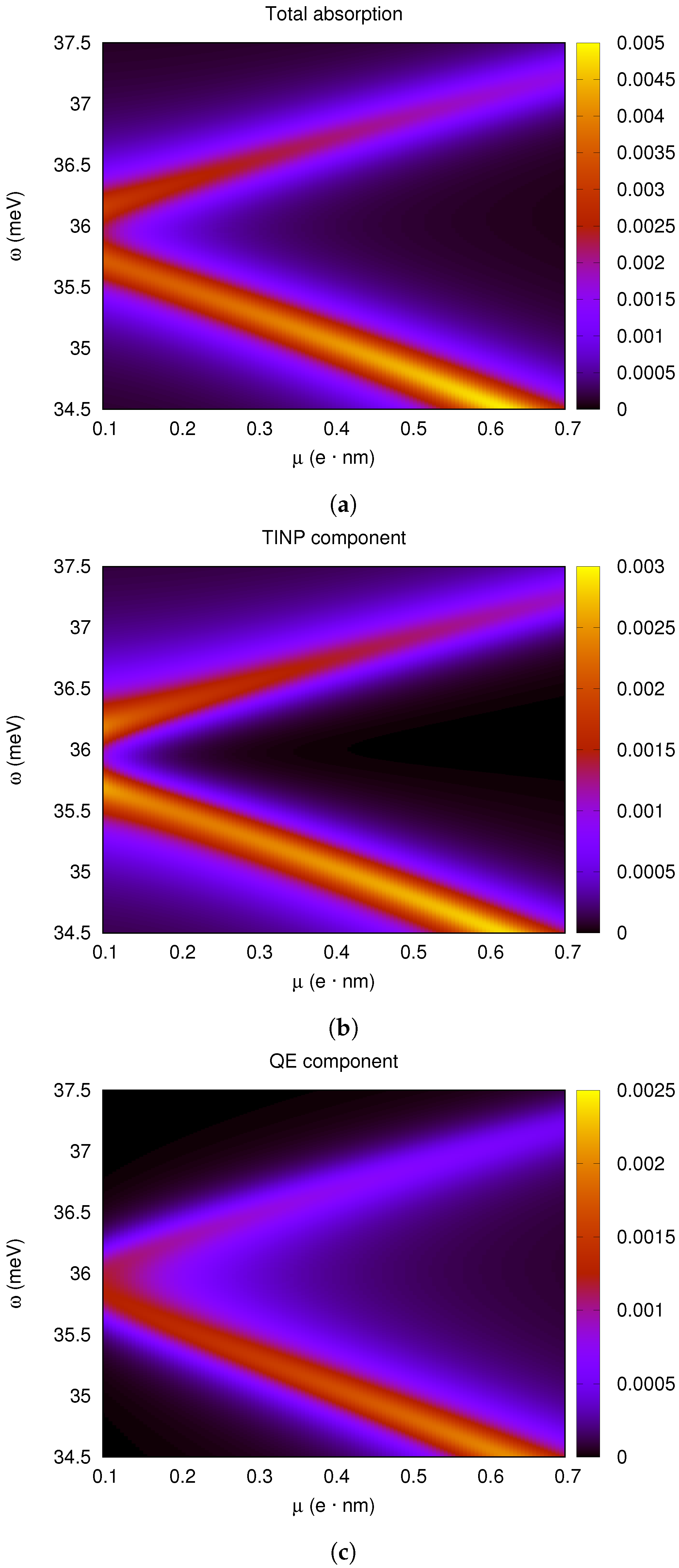
Figure 8.
Separation distance and splitting. The heatmaps show the power absorption ( W) in the system as a function of the exciting light frequency (meV) (vertical axis) and the separation between the two particles R (nm) (horizontal axis). A splitting arises as the separation distance R between the particles becomes small enough. The QE transition frequency was set to meV in order to coincide with the SToP mode position, and the dipole moment was set to e·nm. From the top down, the figures show (a) the total absorption, (b) the TINP component and (c) the QE component of absorption.

Figure 9.
QE dipole moment and splitting. The heatmaps show the power absorption ( W) in the system as a function of the exciting light frequency (meV) (vertical axis) and the dipole moment of the QE (horizontal axis), for a separation distance nm. A splitting arises and grows as the dipole moment is incresed. We note that The QE transition frequency was set to meV in order to coincide with the SToP mode position. From the top down, the figures show (a) the total absorption, (b) the TINP component and (c) the QE component of absorption.

Disclaimer/Publisher’s Note: The statements, opinions and data contained in all publications are solely those of the individual author(s) and contributor(s) and not of MDPI and/or the editor(s). MDPI and/or the editor(s) disclaim responsibility for any injury to people or property resulting from any ideas, methods, instructions or products referred to in the content. |
© 2024 by the authors. Licensee MDPI, Basel, Switzerland. This article is an open access article distributed under the terms and conditions of the Creative Commons Attribution (CC BY) license (https://creativecommons.org/licenses/by/4.0/).
Share and Cite
MDPI and ACS Style
Kountouris, G.; Yannopapas, V. Surface Topological Plexcitons: Strong Coupling in a Bi2Se3 Topological Insulator Nanoparticle-Quantum Dot Molecule. Optics 2024, 5, 101-120. https://0-doi-org.brum.beds.ac.uk/10.3390/opt5010008
AMA Style
Kountouris G, Yannopapas V. Surface Topological Plexcitons: Strong Coupling in a Bi2Se3 Topological Insulator Nanoparticle-Quantum Dot Molecule. Optics. 2024; 5(1):101-120. https://0-doi-org.brum.beds.ac.uk/10.3390/opt5010008
Chicago/Turabian StyleKountouris, George, and Vassilios Yannopapas. 2024. "Surface Topological Plexcitons: Strong Coupling in a Bi2Se3 Topological Insulator Nanoparticle-Quantum Dot Molecule" Optics 5, no. 1: 101-120. https://0-doi-org.brum.beds.ac.uk/10.3390/opt5010008