

Theoretical Study of Doping in GaOOH for Electronics Applications

Department of Electrical and Mechanical Engineering, Nagoya Institute of Technology, Gokiso, Showa, Nagoya 466-8555, Japan
Electron. Mater. 2023, 4(4), 148-157; https://0-doi-org.brum.beds.ac.uk/10.3390/electronicmat4040013
Submission received: 29 August 2023
/
Revised: 5 October 2023
/
Accepted: 9 November 2023
/
Published: 10 November 2023
(This article belongs to the Special Issue Metal Oxide Semiconductors for Electronic Applications)
Abstract
:GaOOH, having a bandgap of 4.7–4.9 eV, can be regarded as one of several ultrawide-bandgap (UWBG) semiconductors, although it has so far mainly been used as a precursor material of Ga2O3. To examine the possibility of valence control and application in electronics, impurity levels in GaOOH are investigated using the first-principles density-functional theory calculation. The density values of the states of a supercell including an impurity atom are calculated. According to the results, among the group 14 elements, Si is expected to introduce a shallow donor level, i.e., a free electron is introduced. On the other hand, Ge and Sn introduce a localized state about 0.7 eV below the conduction band edge, and thus cannot act as an effective donor. While Mg and Ca can introduce a free hole and act as a shallow acceptor, Zn and Cd introduce acceptor levels away from the valence band. The transition metal elements (Fe, Co, Ni, Cu) are also considered, but none of them are expected to act as a shallow dopant. Thus, the results suggest that the carrier concentration can be controlled if Si is used for n-type doping, and Mg and Ca for p-type doping. Since GaOOH can be easily deposited using various chemical techniques at low temperatures, GaOOH will potentially be useful for transparent electronic devices.
1. Introduction
Ultrawide-bandgap (UWBG) semiconductors have been extensively demonstrated to improve the performance of power devices and deep UV optoelectronic devices [1,2]. Ga2O3 is one of the most promising UWBG materials, and has garnered significant attention [3,4]. Various crystal growth techniques have been used to fabricate bulk crystals and thin films, and their basic properties have been investigated in detail. Conductivity has been controlled by impurity doping, and it has been found that groups 14 and 7 elements can be shallow donors [5,6]. On the other hand, it is generally agreed that substitutional acceptor impurities (groups 2, 5, and 12) all have deep levels, and thus will not lead to significant p-type conductivity [6,7,8].
In addition to Ga2O3 bulk crystals and thin films, various types of Ga2O3 nanostructures have also been studied and applied for catalysts and gas sensors [9,10,11]. To fabricate the nanostructure Ga2O3, GaOOH nanostructures were first fabricated via wet chemical processes in most cases, and then converted into Ga2O3 via thermal annealing; GaOOH is converted to Ga2O3 at temperatures above 450 °C. Several comprehensive review papers have been published on syntheses of Ga2O3 via calcining GaOOH nanomaterials obtained using wet chemical approaches [9,10,11]. Thus, so far, GaOOH has been utilized as a precursor material for Ga2O3.
GaOOH itself, having a bandgap of 4.7–4.9 eV [12,13], is also a UWBG material; in fact, there are a few papers in which GaOOH is applied in a photocatalyst and in gas sensors as a semiconductor [12,13,14,15]. GaOOH can be synthesized easily using various wet chemical processes at low temperatures, and is well stable at room temperature. Its conversion to Ga2O3 begins at temperatures above 450 °C, as mentioned above. Thus, GaOOH may potentially be useful for transparent electronics applications wherein wide-bandgap semiconductor films need to be fabricated on transparent substrates such as glass or plastic sheets. Recently, band structures of 2D GaOOH have been studied theoretically for optoelectron application [16]. However, no study has attempted to apply bulk GaOOH for electronic devices such as diodes and transistors.
For electronics applications, conductivity control via impurity doping is essential. In this work, the possibility of conductivity control using impurity doping in GaOOH is analyzed based on a first-principles density-functional theory (DFT) calculation. DFT calculations have been extensively used to study both the bulk and surface properties of a wide range of materials [17,18,19,20]. As an initial survey of possible donor and acceptor impurities, the density of states (DOS) of doped GaOOH is calculated. The DOS of doped Ga2O3 is also calculated and compared with that of doped GaOOH. The results indicate that some impurities will have shallow donor or acceptor levels in GaOOH.
2. Calculation
GaOOH has an orthorhombic structure (α-GaOOH) with lattice constants a = 0.992 nm, b = 0.302 nm, c = 0.457 nm [21]. Each Ga atom is bonded to four O atoms, and each O atom is bonded to two Ga atoms, and an H atom is bonded to half of the O atoms. To simulate a doped material, a 1 × 3 × 2 super cell (96 atoms) was considered; the super cell is rectangular, with a dimension of about 1 nm in each direction. One atom in the super cell was replaced with an impurity atom. For comparison, the calculation was also carried out for undoped and doped β-Ga2O3, which is known to be the most stable crystal structure of Ga2O3. A 1 × 2 × 1 super cell (40 atoms) was considered, as in a previous similar DFT study by Tang et al. [22]. Crystal structure figures of α-GaOOH and β-Ga2O3, generated using the software CrystalMaker, are shown in Figure 1. The local densities of states (LDOS) are also calculated using a limited number of k-points (3 × 2 × 2) of the supercell.
The software PHASE (ver.11.0, University of Tokyo, Tokyo, Japan) was used for the DFT calculations based on the pseudopotential method with generalized gradient approximation (GGA) [23]. Norm-conserving pseudopotential was used for H, Mg and Si, and ultrasoft pseudopotential was used for the other elements. The kinetic energy cutoff of the basis was 272 eV (20 Rydberg). It was confirmed for some cases that variation in the cut-off energy did not significantly affect the conclusions of the calculations. Values from the literature were used for the lattice constants, and the atom positions in the supercell were optimized with the force convergence criterion of 8 × 10⁻² eV/Å. For the preliminary screening of impurity levels, DOS was calculated for the neutral cell. The lattice relaxation accompanying ionization was not considered.
According to a common doping strategy in semiconductor technology, elements with one more or one less valence electron than the matrix element are designated impurities. However, heavy elements, which are not usually used for semiconductor technology, were not considered. In addition, the transition elements used for doping in Ga2O3 were also considered.
3. Results
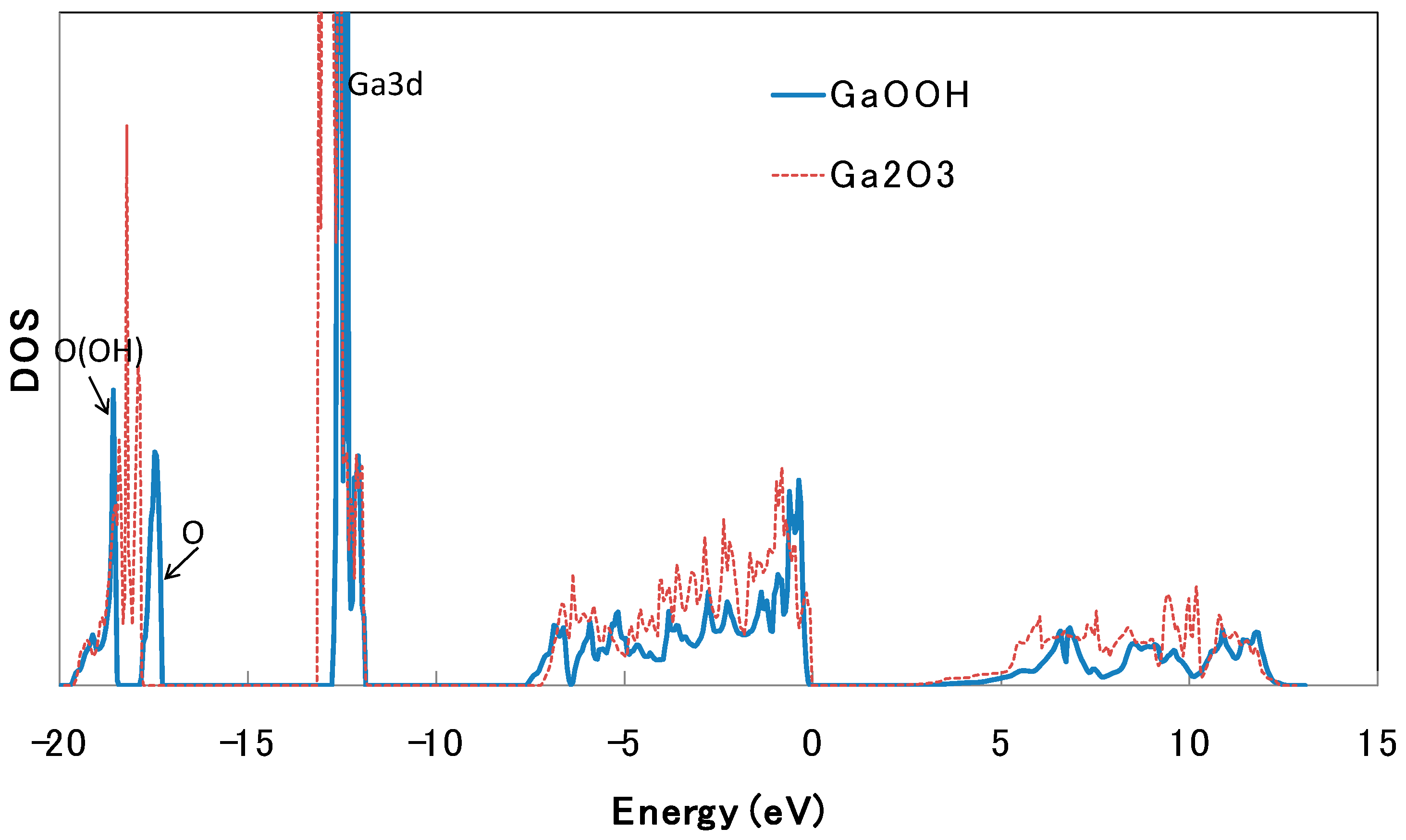
Figure 2 shows calculated DOS for undoped GaOOH and Ga2O3. The origin of the energy (horizontal scale) is the energy of the uppermost filled states, i.e., the Fermi level. For GaOOH, the lowest-energy peak is due to the O atom (2s orbital) bonded to H (hydroxyl group), and the next peak due to the O atom not bonded to H. The peak around −12 eV is attributed to the Ga3d states. For both GaOOH and Ga2O3, the bandgap appears to be about 3.0 eV, while the literature values of their bandgap are 4.7–4.9 eV. Thus, the calculated bandgaps are significantly smaller than the literature values. This is due to the insufficient correction of exchange–correlation energy in the GGA-DFT calculation. In addition, in DFT calculation, the ground-state energy and single-particle density are obtained, and the bandgap energy is not necessarily accurate, even if an exact exchange–correlation potential is used. Considering the underestimation of the bandgap, it can be expected that the depth of the impurity levels will also tend to be underestimated.
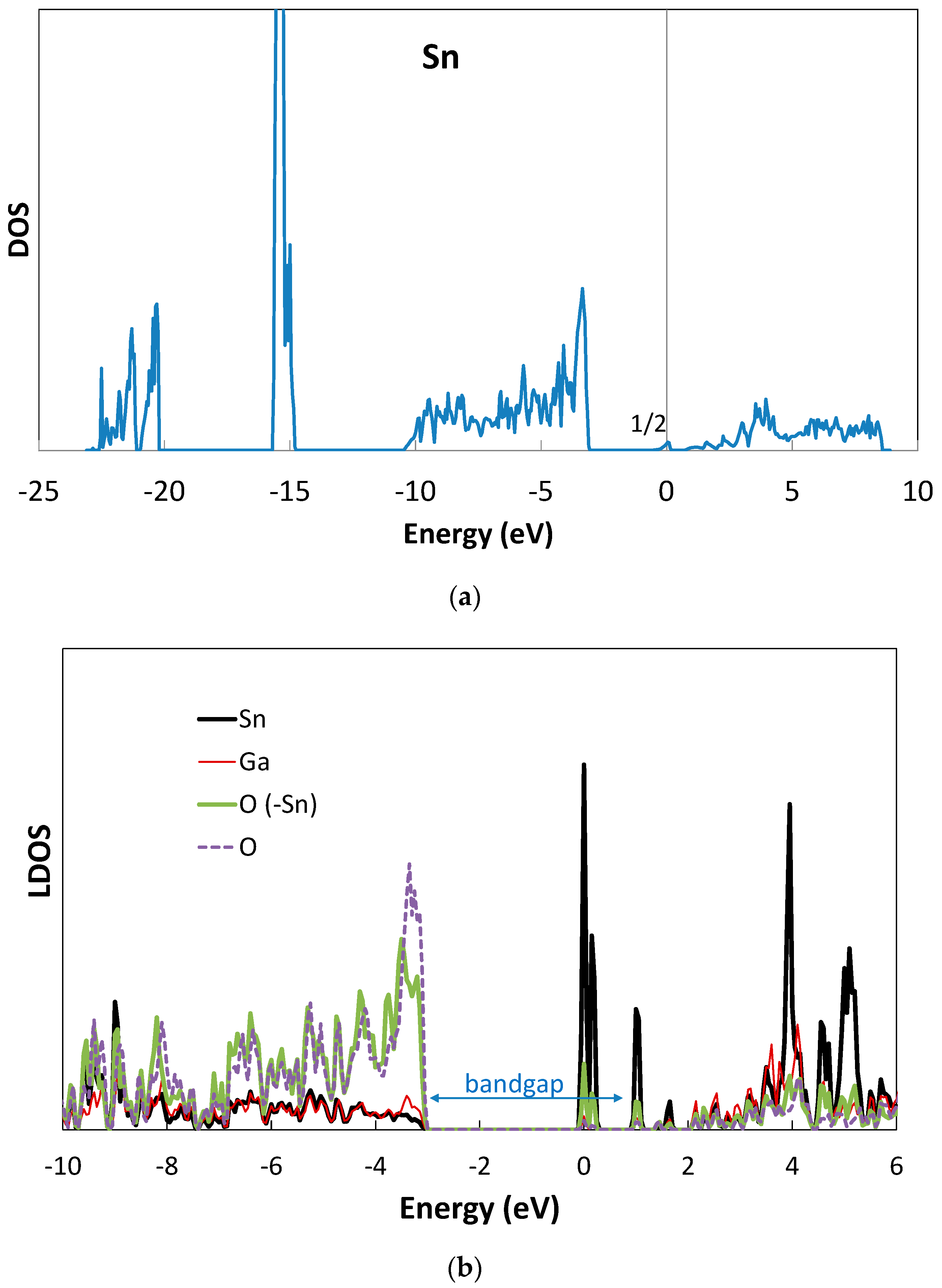
Group 14 elements may be expected to act as a donor when they replace Ga. Among the three group 14 elements (Si, Ge, Sn), only Si is expected to act as a shallow donor in GaOOH; the Fermi level is located above the conduction band edge Ec, as shown in Figure 3a. The LDOS of the Si-doped GaOOH near the bandgap are shown in Figure 3b. Since The LDOS were calculated using a limited number of k-points; smooth curves of LDOS could not be obtained. The approximate range of the bandgap is also shown in the figures. As can be seen from the figure, no localized gap states are formed. Thus, the wave function of an extra electron introduced by Si is not localized, i.e., Si acts as a shallow donor. The valence band top is mostly contributed by the O 2p orbital, while the conduction band bottom is contributed by the Ga 4s orbital with the additional contribution of O. On the other hand, Ge and Sn introduce half-filled states about 0.7 eV-below Ec, and thus will be a deep donor, unable to contribute to n-type conduction. The results for Sn are shown in Figure 4, and those for Ge are similar. According to the LDOS of Sn-doped GaOOH shown in Figure 4b, the gap states localized around the Sn atom are introduced, as shown by the bold black line. In the figures, “O (-Sn)” means the O atom bonded to Sn. The LDOS of the gap states are also significant at the neighboring O atoms, and thus the wave functions of the gap states are extended to the neighboring O atoms.
For Ga2O3, it has been shown theoretically and experimentally that both Si and Sn are a shallow donor. Actually, according to our calculations, both Si and Sn are expected to be a shallow donor. Our results for Si and Sn-doped Ga2O3 agree with previous similar calculations [22]. Sn introduces a shallow level in Ga2O3 and a deep level in GaOOH, i.e., the energy level of Sn is deeper in GaOOH than in Ga2O3.
As group 17 elements, F and Cl were considered. According to the present calculation, a Cl atom replacing an O atom (not bonded to H) will act as a shallow donor, whereas F at the O site will be a deep donor, having a half-filled level 0.5 eV-below Ec. This is in contrast to the results for Ga2O3; for Ga2O3, it is shown theoretically and experimentally that both F and Cl are shallow donors.
Group 17 element atoms may replace a hydroxyl group OH in GaOOH. Both F and Cl atoms replacing OH introduce filled states in the lower half of the bandgap, and thus will not act as a donor or acceptor. The relative stability of those two sites (O site and OH site) cannot be examined using the present calculation. Since the control of the site occupation is not established for F and Cl, they will not be readily used as a donor.
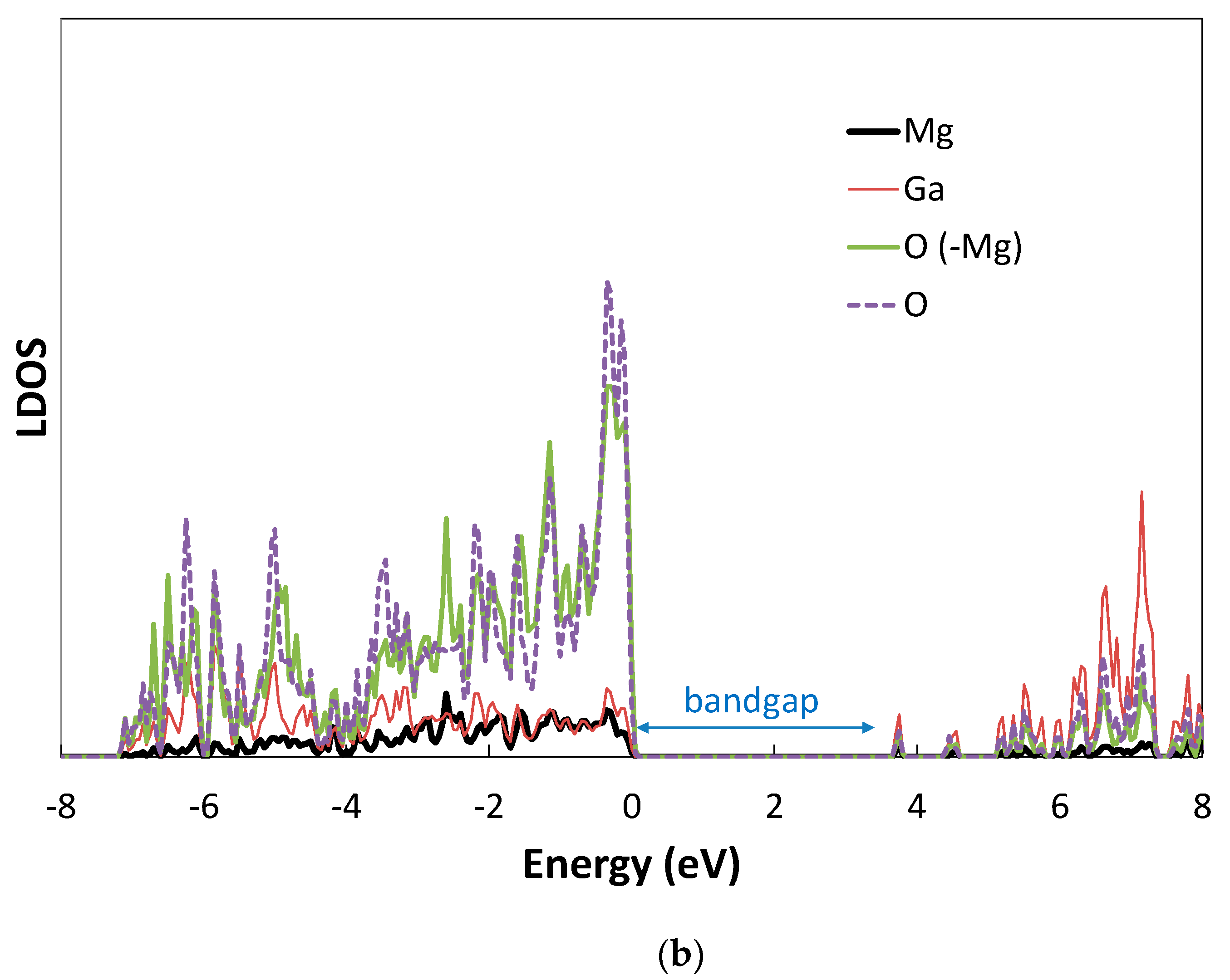
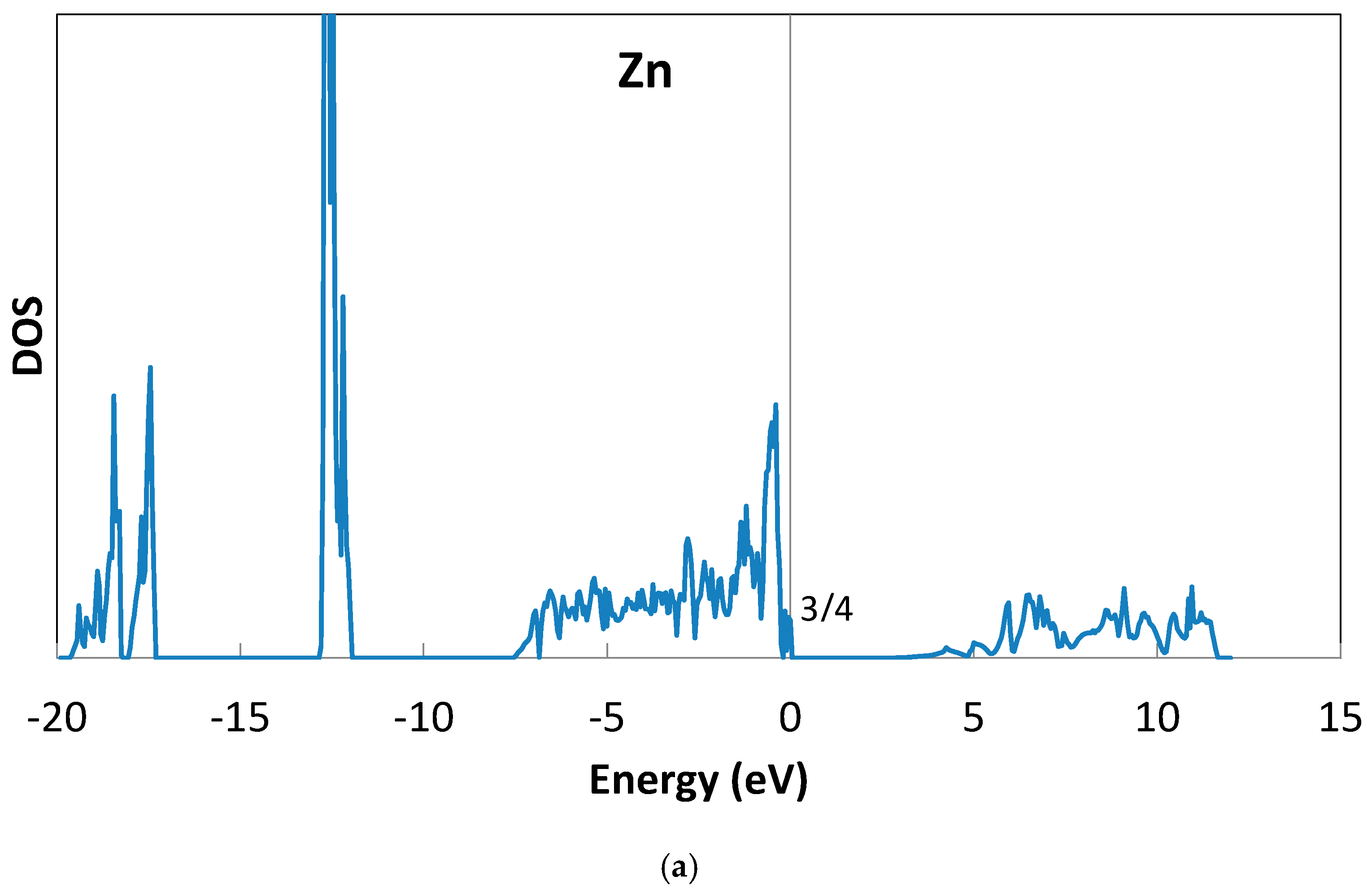
Groups 2 and 12 element atoms at the Ga site may be potential acceptors, considering their valence electron number. According to the present calculation, group 2 elements Mg and Ca will be shallow acceptors in GaOOH, while group 12 elements Zn and Cd are rather deep acceptors, with levels 0.2–0.3 eV apart from the valence band edge Ev. The results for Mg are shown in Figure 5. The Fermi level is located just below Ev, and there is a hole in the valence band, i.e., Mg acts as a shallow acceptor. The LDOS of the Mg-doped GaOOH are shown in Figure 5b. As in the case with Si doping, no localized states are found. The results for Zn are shown in Figure 6. The gap states are found about 0.2 eV away from Ev. According to Figure 6b, LDOS of the gap states are comparable for both Zn and neighboring O atoms, i.e., the wave function is localized within the cluster of the Zn and surrounding O atoms. The large peak around −4.5 eV, shown by the bold black line, corresponds to states due to the 3d orbital of Zn. On the other hand, for Ga2O3, both Mg and Zn are expected to be a shallow accepter according to the present calculation and the previous DFT-GGA study [22]. However, the energy levels of Mg and Zn obtained using more elaborated hybrid functional calculation are much deeper, and it was also found experimentally that they are in fact a deep acceptor, being unable to result in sufficient p-type conduction [6,7,8]. Considering the underestimated energy in the present GGA calculation, Zn and Cd will in fact be an acceptor too deep to be employed, since their energy levels are even deeper in GaOOH than in Ga2O3. Mg in GaOOH is a shallow acceptor in our calculation, but this needs to be confirmed experimentally, and also via a hybrid functional calculation.
The group 15 element N at the O site may be another candidate of acceptor. In the present calculation, it is shown that the depth of the acceptor level of N in GaOOH is comparable to that of the group 12 elements (for both the O sites). Thus, N will not be a shallow acceptor in GaOOH either. For Ga2O3, it is found both theoretically and experimentally that N introduces deep acceptor levels and cannot lead to significant p-type conduction [6,7].
Several transition metal elements are also considered (Fe, Co, Ni, Cu). Among them, Cu is known to be an acceptor in some wide-bandgap oxides and hydroxides [24,25]. The calculation results show that all of the transition elements considered here do not introduce any shallow donor or acceptor levels. The Cu acceptor levels are more than 1 eV apart from Ev. Fe, Ni, and Cu have partially filled gap states, and could even remove carriers (increase resistivity) in both n and p-type GaOOH. Those transition metals also introduce gap states and thus will remove carriers in Ga2O3; the results for Ga2O3 are consistent with those in the previous DFT-GGA study [22].
The energy levels obtained are summarized in Table 1. The energy levels calculated in this work for Ga2O3 agree fairly well with those of the previous DFT study based on GGA [22]. As noted above, the depth of gap states will be underestimated in the present calculation. The purpose of the present work is an initial screening of impurities for doping; one can exclude impurities with deep levels in the present calculation. For n-type doping, only Si will be a candidate. Cl at the O site may be shallow, but Cl can also replace OH, being inactive. For p-type doping, group 2 elements Mg and Ca can be used according to the present results. Hydroxides of those two elements can be easily synthesized using chemical techniques, and thus they may be doped into GaOOH in chemical syntheses.
The supercell considered corresponds to a very high doping level of the order of 1021 cm−3. In addition, periodicity is assumed in the arrangement of impurity atoms. Those are inherent problems in supercell calculation, and their effects on the results are difficult to predict and discuss.
If the conductivity of GaOOH can be controlled using impurity doping, GaOOH thin films could be used for diodes and transistors in transparent electronics applications. For transparent electronics applications, devices need to be fabricated on plastic or glass sheets, and thus semiconductor thin films should be deposited at low temperatures. GaOOH can be deposited via various chemical techniques at low temperatures, and thus would be well suited for transparent electronics applications.
4. Conclusions
Energy levels introduced by impurities in GaOOH have been investigated based on first-principles DFT calculation. The density of states of a supercell including an impurity atom have been calculated. According to the results, Si is expected to introduce a shallow donor level, whereas Ge and Sn introduce a localized state about 0.7 eV below the conduction band edge, and thus cannot act as donors. While Mg and Ca can introduce a free hole and act as a shallow acceptor, Zn and Cd introduce acceptor levels away from the valence band. The transition metal elements (Fe, Co, Ni, Cu) are expected to introduce deep levels within the bandgap. Thus, the carrier concentration can be controlled if Si is used for n-type doping, and Mg and Ca for p-type doping.
Funding
This work was partly supported by JSPS Kakenhi Grant Number 22K05268.
Data Availability Statement
The data presented in this study are available on request from the corresponding author.
Conflicts of Interest
The author declares no conflict of interest.
References
- Tsao, J.Y.; Chowdhury, S.; Hollis, M.A.; Jena, D.; Johnson, N.M.; Jones, K.A.; Kaplar, R.J.; Rajan, S.; Van de Walle, C.G.; Bellotti, E.; et al. Ultrawide-Bandgap Semiconductors: Research Opportunities and Challenges. Adv. Electron. Mater. 2018, 4, 1600501. [Google Scholar] [CrossRef]
- Wong, M.H.; Bierwagen, O.; Kaplar, R.J.; Umezawa, H. Ultrawide-bandgap semiconductors: An overview. J. Mater. Res. 2021, 36, 4601. [Google Scholar] [CrossRef]
- Higashiwaki, M.; Sasaki, K.; Murakami, H.; Kumagai, Y.; Koukitu, A.; Kuramata, A.; Masui, T.; Yamakoshi, S. Recent progress in Ga2O3 power devices. Semicond. Sci. Technol. 2016, 31, 034001. [Google Scholar] [CrossRef]
- Guo, D.; Guo, Q.; Chen, Z.; Wu, Z.; Li, P.; Tang, W. Review of Ga2O3-based optoelectronic devices. Mater. Today Phys. 2019, 11, 100157. [Google Scholar] [CrossRef]
- Varley, J.B.; Weber, J.R.; Janotti, A.; Van de Walle, C.G. Oxygen vacancies and donor impurities in β-Ga2O3. Appl. Phys. Lett. 2010, 97, 142106. [Google Scholar] [CrossRef]
- Tadjer, M.J.; Lyons, J.L.; Nepal, N.; Freitas, J.A., Jr.; Koehler, A.D.; Foster, G.M. Review—Theory and Characterization of Doping and Defects in β-Ga2O3. ECS J. Solid St. Sci. Technol. 2019, 8, Q3187. [Google Scholar]
- Lyons, J.L. A survey of acceptor dopants for β-Ga2O3. Semicon. Sci. Technol. 2018, 33, 05LT02. [Google Scholar] [CrossRef]
- Kyrtsos, A.; Matsubara, M.; Bellotti, E. On the feasibility of p-type Ga2O3. Appl. Phys. Lett. 2018, 112, 032108. [Google Scholar] [CrossRef]
- Chiang, J.L.; Yadlapalli, B.K.; Chen, M.I.; Wuu, D.S. A Review on Gallium Oxide Materials from Solution Processes. Nanomaterials 2022, 12, 3601. [Google Scholar] [CrossRef]
- Jamwal, N.S.; Kiani, A. Gallium Oxide Nanostructures: A Review of Synthesis, Properties and Applications. Nanomaterials 2022, 12, 2061. [Google Scholar] [CrossRef]
- Shi, F.; Qiao, H. Preparations, properties and applications of gallium oxide nanomaterials—A Review. Nano Select. 2022, 3, 348. [Google Scholar] [CrossRef]
- Sun, M.; Li, D.; Zhang, W.; Fu, X.; Shao, Y.; Li, W.; Xiao, G.; He, Y. Rapid microwave hydrothermal synthesis of GaOOH nanorods with photocatalytic activity toward aromatic compounds. Nanotechnology 2010, 21, 355601. [Google Scholar] [CrossRef] [PubMed]
- Xu, X.; Bi, K.; Huang, K.; Liang, C.; Lin, S.; Wang, W.J.; Yang, T.Z.; Liu, J.; Fan, D.Y.; Yang, H.J.; et al. Controlled fabrication of α-GaOOH with a novel needle-like submicron tubular structure and its enhanced photocatalytic performance. J. Alloys Comp. 2015, 644, 485. [Google Scholar] [CrossRef]
- Hong, S.; Rhee, C.K.; Sohn, Y. Photoluminescence, electro- and thermal catalytic properties of bare and Eu(III)-doped GaOOH, α- and β-Ga2O3 nanorods. J. Alloys Compd. 2018, 774, 11. [Google Scholar] [CrossRef]
- Pilliadugula, R.; Krishnan, N.G. Gas sensing performance of GaOOH and β-Ga2O3 synthesized by hydrothermal method: A comparison. Mater. Res. Exp. 2019, 6, 025027. [Google Scholar] [CrossRef]
- Upadhyay, D.; Joshi, N.; Jha, P.K. Two dimensional hexagonal GaOOH: A promising ultrawide bandgap semiconductor for smart optoelectronic applications. Chem. Phys. Lett. 2021, 765, 138310. [Google Scholar] [CrossRef]
- Zhang, H.P.; Zhang, R.; Sun, C.; Jiao, Y.; Zhang, Y. CO2 reduction to CH4 on Cu-doped phosphorene: A first-principles study. Nanoscale 2021, 13, 20541. [Google Scholar] [CrossRef]
- Yu, X.; Xie, J.; Dong, H.; Liu, Q.; Li, Y. Effects of oxygen defects on electronic band structures and dopant migration in Sn-doped TiO2 by density functional studies. Chem. Phys. Lett. 2020, 754, 137732. [Google Scholar] [CrossRef]
- Zhang, R.; Zhang, Y.; Liu, L.; Li, X.; Tang, Y.; Ni, Y.; Sun, C.; Zhang, H. Selective bimetallic sites supported on graphene as a promising catalyst for CO2 Reduction: A first-principles study. Appl. Surf. Sci. 2022, 30, 152472. [Google Scholar] [CrossRef]
- Hou, J.; Chen, M.; Zhou, Y.; Bian, L.; Dong, F.; Tang, Y.; Ni, Y.; Zhang, H. Regulating the effect of element doping on the CO2 capture performance of kaolinite: A density functional theory study. Appl. Surf. Sci. 2020, 512, 145642. [Google Scholar] [CrossRef]
- The Materials Project. Available online: https://materialsproject.org/ (accessed on 20 December 2022).
- Tang, C.; Sun, J.; Lin, N.; Jia, Z.; Mu, W.; Tao, X.; Zhao, X. Electronic structure and optical property of metal-doped Ga2O3: A first principles study. RSC Adv. 2016, 6, 78322. [Google Scholar] [CrossRef]
- Perdew, J.P.; Burke, K.; Ernzerholf, M. Generalized Gradient Approximation Made Simple. Phys. Rev. Lett. 1996, 77, 3865. [Google Scholar] [CrossRef] [PubMed]
- Keikhaei, M.; Ichimura, M. n-type and p-type semiconducting Cu-doped Mg(OH)2 thin film. Semicond. Sci. Technol. 2020, 35, 035020. [Google Scholar] [CrossRef]
- Keikhaei, M.; Ichimura, M. Fabrication of p-type Transparent (CuZn)O Thin Films by the Electrochemical Deposition Method. Int. J. Electrochem. Sci. 2020, 15, 156. [Google Scholar] [CrossRef]
Figure 1.
Crystal structures of (a) α-GaOOH and (b) β-Ga2O3. The unit cell is indicated by the blue dashed line, and the atoms located outside of the unit cell are shown with weaker color. The unit cell of GaOOH contains four Ga atoms, eight O atoms, and four H atoms. The cell of Ga2O3 contains eight Ga atoms and twelve O atoms.

Figure 2.
DOS for undoped GaOOH and Ga2O3.

Figure 3.
(a) DOS and (b) LDOS of Si-doped GaOOH. “O (-Si)” means an O atom bonded to Si.

Figure 4.
(a) DOS and (b) LDOS of Sn-doped GaOOH. “O (-Sn)” means an O atom bonded to Sn.

Figure 5.
(a) DOS and (b) LDOS of Mg-doped GaOOH.


Figure 6.
(a) DOS and (b) LDOS of Zn-doped GaOOH.


Table 1.
Gap states introduced by impurities in GaOOH. (M/N) is the occupation of the impurity levels; N is the number of the states, and M the number of occupying electrons. “Shallow donor/acceptor” means that a free carrier is introduced, i.e., the Fermi level is located in the band. For comparison, the levels in β-Ga2O3 calculated in the present study based on GGA and those obtained on the basis of the hybrid functional [5,7,8] are also given. (In Ga2O3, there are two inequivalent Ga sites and three inequivalent O sites. The levels were calculated for those different atom sites, and in the table, the shallowest level is listed for each impurity).
| GaOOH | Ga2O3 | |||
|---|---|---|---|---|
| GGA | Hybrid [5,7,8] | |||
| group 14 | Si | shallow donor | shallow donor | shallow donor |
| Ge | Ec − 0.75 (1/2) | |||
| Sn | Ec − 0.7 (1/2) | shallow donor | shallow donor | |
| group 17 | F (O) | Ec − 0.5 (1/2) | shallow donor | shallow donor |
| F (OH) | Ev + 0.35 (2/2) | |||
| Cl (O) | shallow donor | shallow donor | shallow donor | |
| Cl (OH) | Ev + 0.6 (2/2) | |||
| group 2 group 12 | Mg | shallow acceptor | shallow acceptor | Ev + 1.05 |
| Ca | shallow acceptor | shallow acceptor | ||
| Zn | Ev + 0.2 (1/2) | shallow acceptor | Ev + 1.22 | |
| Cd | Ev + 0.3 (3/4) | shallow acceptor | ||
| group 15 | N | Ev + 0.2 (3/4) | Ev + 0.1 | |
| N-H | Ev + 0.35 (1/2) | |||
| transition metals | Fe | Ec − 1.0 (5/6) | ||
| Co | Ev + 1.3 (6/6) | Ev + 1~1.5 | ||
| Ni | Ec − 1.0 (1/2), −0.5 (0/2) | Ev + 1.0 | ||
| Cu | Ev + 0.9 (2/2), +1.2 (0/2) | Ev + 0.15 | ||
Disclaimer/Publisher’s Note: The statements, opinions and data contained in all publications are solely those of the individual author(s) and contributor(s) and not of MDPI and/or the editor(s). MDPI and/or the editor(s) disclaim responsibility for any injury to people or property resulting from any ideas, methods, instructions or products referred to in the content. |
© 2023 by the author. Licensee MDPI, Basel, Switzerland. This article is an open access article distributed under the terms and conditions of the Creative Commons Attribution (CC BY) license (https://creativecommons.org/licenses/by/4.0/).
Share and Cite
MDPI and ACS Style
Ichimura, M. Theoretical Study of Doping in GaOOH for Electronics Applications. Electron. Mater. 2023, 4, 148-157. https://0-doi-org.brum.beds.ac.uk/10.3390/electronicmat4040013
AMA Style
Ichimura M. Theoretical Study of Doping in GaOOH for Electronics Applications. Electronic Materials. 2023; 4(4):148-157. https://0-doi-org.brum.beds.ac.uk/10.3390/electronicmat4040013
Chicago/Turabian StyleIchimura, Masaya. 2023. "Theoretical Study of Doping in GaOOH for Electronics Applications" Electronic Materials 4, no. 4: 148-157. https://0-doi-org.brum.beds.ac.uk/10.3390/electronicmat4040013