Water Photo-Electrooxidation Using Mats of TiO2 Nanorods, Surface Sensitized by a Metal–Organic Framework of Nickel and 1,2-Benzene Dicarboxylic Acid

 ,
,  ,
,  , and
, and 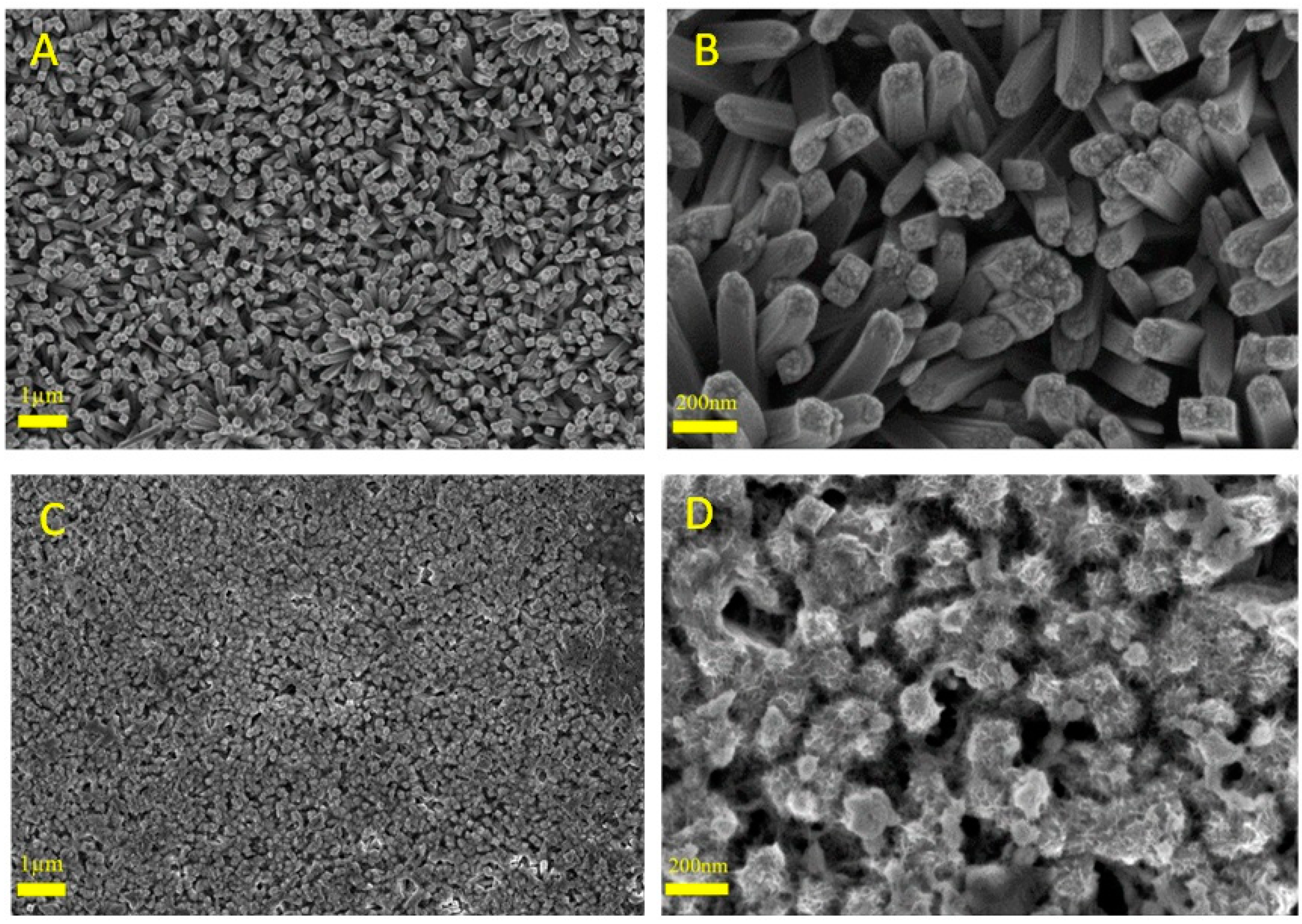
Abstract
:1. Introduction
2. Materials and Methods
2.1. Chemicals
2.2. Fabrication of TDNRs/FTO/Glass Photoelectrodes
2.3. Electrodeposition of Ni Species onto the TDNRs/FTO/Glass Photoelectrodes
2.4. Formation of the Ni-BDCA MOF onto the TDNRs/FTO/Glass Photoelectrodes
2.5. Physical Characterization
2.6. Photo-Electrochemical Measurements
3. Results and Discussion
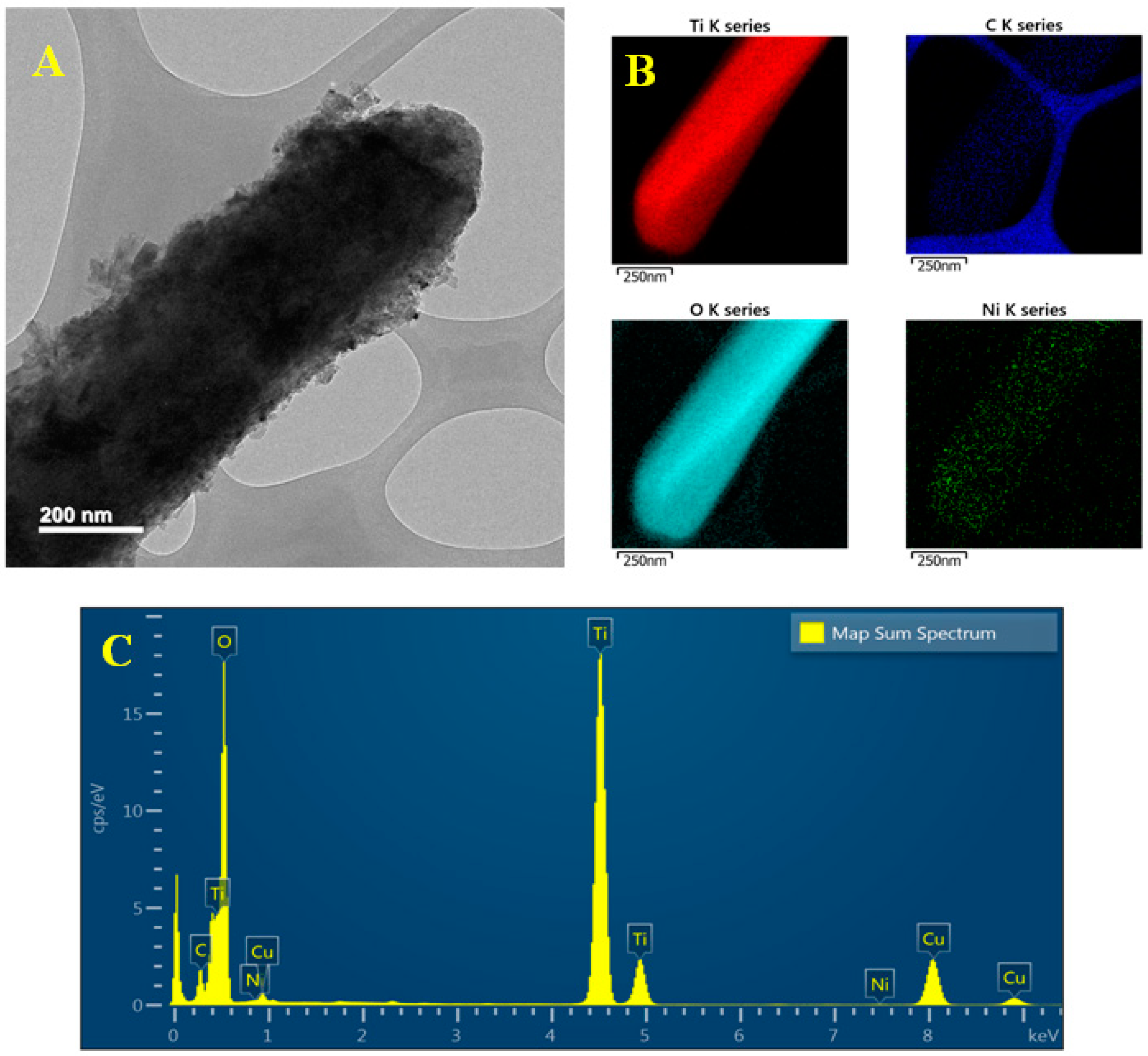
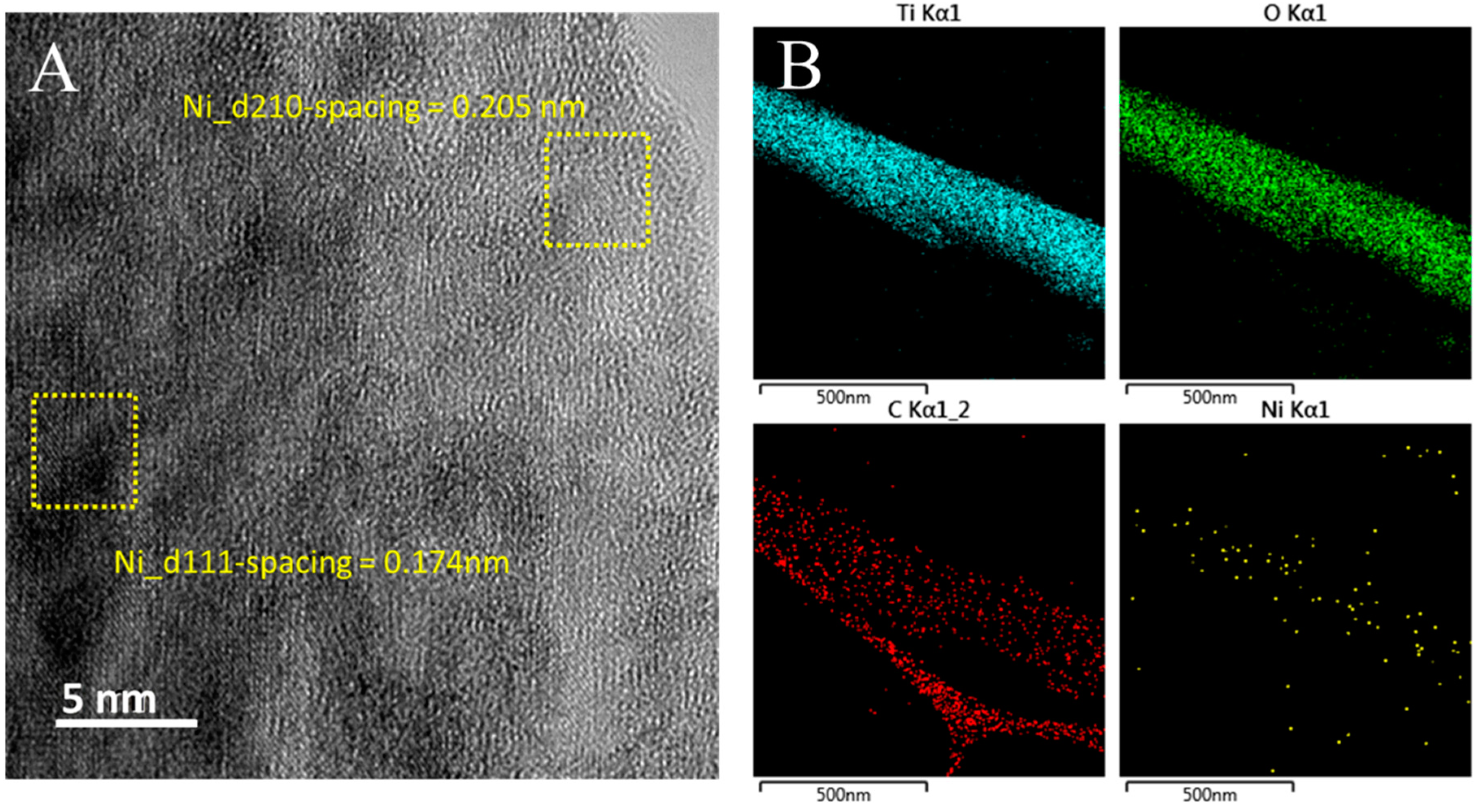
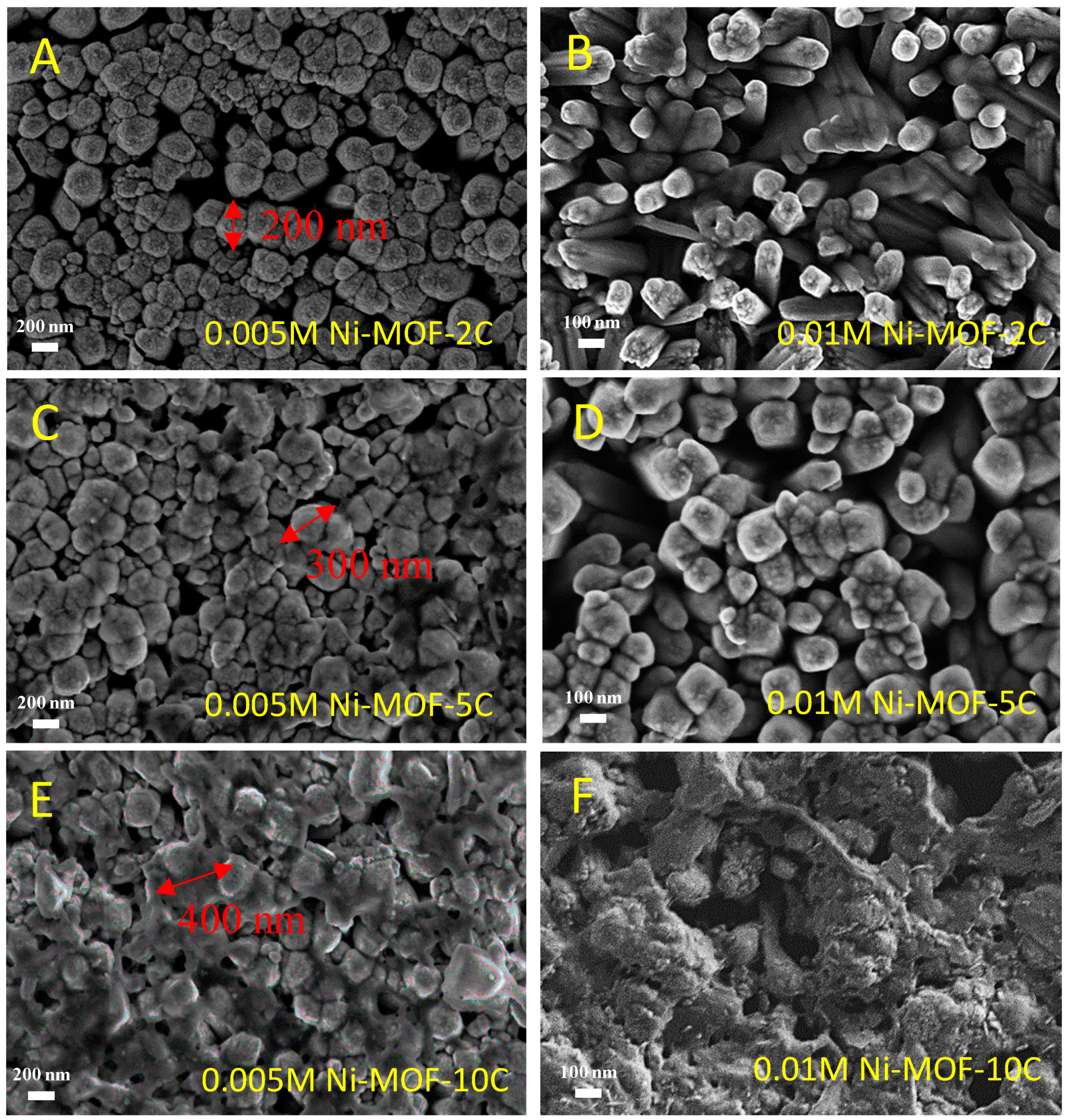
3.1. Structural and Morphological Characterization
3.2. Physico-Chemical Characterization
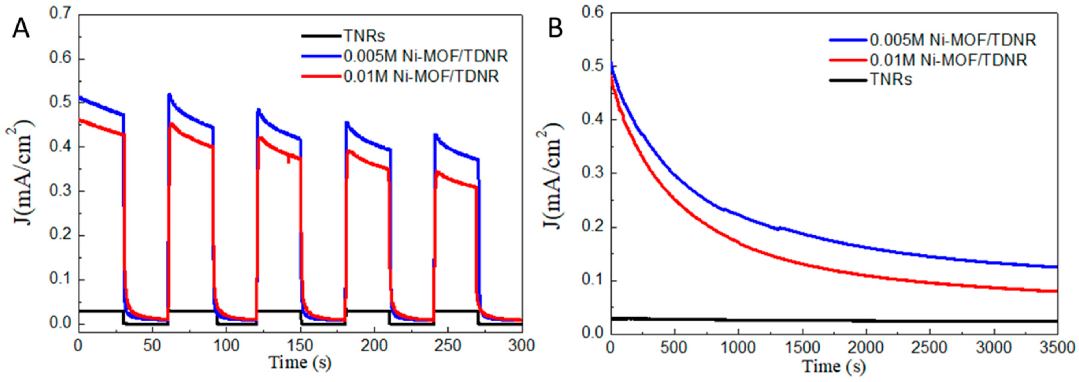
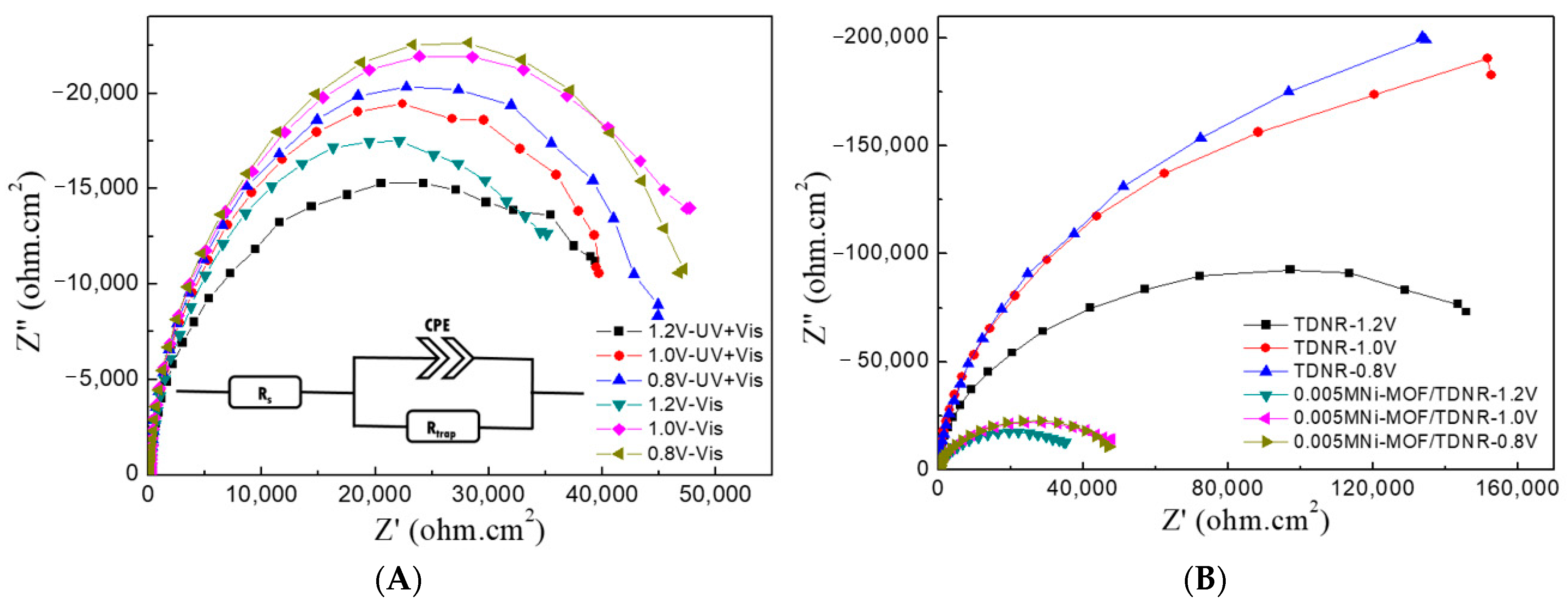
3.3. PEC Analysis
4. Conclusions
Supplementary Materials
Author Contributions
Funding
Data Availability Statement
Acknowledgments
Conflicts of Interest
References
- Crabtree, G.W.; Dresselhaus, M.S.; Buchanan, M.V. The Hydrogen Economy. Phys. Today 2004, 57, 39–44. [Google Scholar] [CrossRef]
- GadelHak, Y.; El Rouby, W.M.; Farghali, A.A. Au-decorated 3D/1D titanium dioxide flower-like/rod bilayers for photoelectrochemical water oxidation. Electrochim. Acta 2019, 306, 185–197. [Google Scholar] [CrossRef]
- Becquerel, A.E. Recherches sur les effets de la radiation chimique de la lumiere solaire au moyen des courants electriques. Comptes Rendus L’acad. Des. Sci. 1839, 9, 1. [Google Scholar]
- Fujishima, A.; Honda, K. Electrochemical Photolysis of Water at a Semiconductor Electrode. Nature 1972, 238, 37–38. [Google Scholar] [CrossRef]
- Lyu, F.; Wang, Q.; Choi, S.M.; Yin, Y. Noble-Metal-Free Electrocatalysts for Oxygen Evolution. Small 2019, 15, e1804201. [Google Scholar] [CrossRef] [Green Version]
- Zou, X.; Zhang, Y. Noble metal-free hydrogen evolution catalysts for water splitting. Chem. Soc. Rev. 2015, 44, 5148–5180. [Google Scholar] [CrossRef]
- Mohan, S.; Mao, Y. Dependence of (Photo)electrochemical Properties on Geometry Factors of Hydrothermally Synthesized Delafossite Copper Gallium Oxide CuGaO2toward Oxygen Evolution Reaction. J. Electrochem. Soc. 2018, 165, H607–H613. [Google Scholar] [CrossRef]
- El Rouby, W.M.; Farghali, A.A. Titania morphologies modified gold nanoparticles for highly catalytic photoelectrochemical water splitting. J. Photochem. Photobiol. A Chem. 2018, 364, 740–749. [Google Scholar] [CrossRef]
- Kegel, J.; Povey, I.M.; Pemble, M.E. Zinc oxide for solar water splitting: A brief review of the material’s challenges and associated opportunities. Nano Energy 2018, 54, 409–428. [Google Scholar] [CrossRef]
- Hassan, M.A.; Johar, M.A.; Yu, S.Y.; Ryu, S.-W. Facile Synthesis of Well-Aligned ZnO Nanowires on Various Substrates by MOCVD for Enhanced Photoelectrochemical Water-Splitting Performance. ACS Sustain. Chem. Eng. 2018, 6, 16047–16054. [Google Scholar] [CrossRef]
- Zhang, Z.; Wang, P. Highly stable copper oxide composite as an effective photocathode for water splitting via a facile electrochemical synthesis strategy. J. Mater. Chem. 2012, 22, 2456–2464. [Google Scholar] [CrossRef]
- Paracchino, A.; Mathews, N.; Hisatomi, T.; Stefik, M.; Tilley, S.D.; Grätzel, M. Ultrathin films on copper(i) oxide water splitting photocathodes: A study on performance and stability. Energy Environ. Sci. 2012, 5, 8673–8681. [Google Scholar] [CrossRef]
- Fiorenza, R.; Bellardita, M.; D’Urso, L.; Compagnini, G.; Palmisano, L.; Scirè, S. Au/TiO2-CeO2 Catalysts for Photocatalytic Water Splitting and VOCs Oxidation Reactions. Catalysts 2016, 6, 121. [Google Scholar] [CrossRef] [Green Version]
- You, D.; Pan, B.; Jiang, F.; Zhou, Y.; Su, W. CdS nanoparticles/CeO2 nanorods composite with high-efficiency visible-light-driven photocatalytic activity. Appl. Surf. Sci. 2016, 363, 154–160. [Google Scholar] [CrossRef]
- Malathi, A.; Madhavan, J.; Ashokkumar, M.; Arunachalam, P. A review on BiVO 4 photocatalyst: Activity enhancement methods for solar photocatalytic applications. Appl. Catal. A Gen. 2018, 555, 47–74. [Google Scholar]
- Zhang, J.; Liu, Z.; Liu, Z. Novel WO3/Sb2S3 Heterojunction Photocatalyst Based on WO3 of Different Morphologies for Enhanced Efficiency in Photoelectrochemical Water Splitting. ACS Appl. Mater. Interfaces 2016, 8, 9684–9691. [Google Scholar] [CrossRef]
- Radzi, A.A.S.M.; Safaei, J.; Teridi, M.A.M. Photoelectrochemical enhancement from deposition of BiVO4 photosensitizer on different thickness layer TiO2 photoanode for water splitting application. Nano-Struct. Nano-Objects 2019, 18, 100274. [Google Scholar] [CrossRef]
- Jeong, K.; Deshmukh, P.R.; Park, J.; Sohn, Y.; Shin, W.G. ZnO-TiO2 Core–Shell Nanowires: A Sustainable Photoanode for Enhanced Photoelectrochemical Water Splitting. ACS Sustain. Chem. Eng. 2018, 6, 6518–6526. [Google Scholar] [CrossRef]
- Silipas, T.D.; Indrea, E.; Dreve, S.; Suciu, R.-C.; Rosu, M.C.; Danciu, V.; Cosoveanu, V.; Popescu, V. TiO2—Based systems for photoelectrochemical generation of solar hydrogen. J. Phys. Conf. Ser. 2009, 182, 012055. [Google Scholar] [CrossRef] [Green Version]
- Shen, S.; Chen, J.; Wang, M.; Sheng, X.; Chen, X.; Feng, X.; Mao, S.S. Titanium dioxide nanostructures for photoelectrochemical applications. Prog. Mater. Sci. 2018, 98, 299–385. [Google Scholar] [CrossRef]
- Bae, D.; Seger, B.; Hansen, O.; Vesborg, P.C.; Chorkendorff, I. Durability testing of photoelectrochemical hydrogen production under day/night light cycled conditions. ChemElectroChem 2019, 6, 106–109. [Google Scholar] [CrossRef]
- Bae, D.; Seger, B.; Vesborg, P.C.; Hansen, O.; Chorkendorff, I. Strategies for stable water splitting via protected photoelectrodes. Chem. Soc. Rev. 2017, 46, 1933–1954. [Google Scholar] [CrossRef] [PubMed] [Green Version]
- Antuch, M.; El Rouby, W.; Millet, P. A comparison of water photo-oxidation and photo-reduction using photoelectrodes surface-modified by deposition of co-catalysts: Insights from photo-electrochemical impedance spectroscopy. Int. J. Hydrog. Energy 2019, 44, 9970–9977. [Google Scholar] [CrossRef]
- Carne-Sanchez, A.; Imaz, I.; Stylianou, K.C.; Maspoch, D. Metal-organic frameworks: From molecules/metal ions to crystals to superstructures. Chemistry 2014, 20, 5192–5201. [Google Scholar] [CrossRef]
- Zhang, W.; Wu, Z.Y.; Jiang, H.L.; Yu, S.H. Nanowire-directed templating synthesis of metal-organic framework nanofibers and their derived porous doped carbon nanofibers for enhanced electrocatalysis. J. Am. Chem. Soc. 2014, 136, 14385–14388. [Google Scholar] [CrossRef] [PubMed]
- Ma, T.Y.; Dai, S.; Jaroniec, M.; Qiao, S.Z. Metal-organic framework derived hybrid Co3O4-carbon porous nanowire arrays as reversible oxygen evolution electrodes. J. Am. Chem. Soc. 2014, 136, 13925–13931. [Google Scholar] [CrossRef] [Green Version]
- Li, Z.; Shao, M.; Zhou, L.; Zhang, R.; Zhang, C.; Wei, M.; Evans, D.G.; Duan, X. Directed Growth of Metal-Organic Frameworks and Their Derived Carbon-Based Network for Efficient Electrocatalytic Oxygen Reduction. Adv. Mater. 2016, 28, 2337–2344. [Google Scholar] [CrossRef]
- Wang, Y.; Li, L.; Liang, H.; Xing, Y.; Yan, L.; Dai, P.; Gu, X.; Zhao, G.; Zhao, X. Superstructure of a Metal-Organic Framework Derived from Microdroplet Flow Reaction: An Intermediate State of Crystallization by Particle Attachment. ACS Nano 2019, 13, 2901–2912. [Google Scholar] [CrossRef]
- Jiao, L.; Seow, J.Y.R.; Skinner, W.S.; Wang, Z.U.; Jiang, H.-L. Metal–organic frameworks: Structures and functional applications. Mater. Today 2019, 27, 43–68. [Google Scholar] [CrossRef]
- Gao, X.; Cui, R.; Ji, G.; Liu, Z. Size and surface controllable metal–organic frameworks (MOFs) for fluorescence imaging and cancer therapy. Nanoscale 2018, 10, 6205–6211. [Google Scholar] [CrossRef]
- Chen, J.; Liu, J.; Xie, J.-Q.; Ye, H.; Fu, X.-Z.; Sun, R.; Wong, C.-P. Co-Fe-P nanotubes electrocatalysts derived from metal-organic frameworks for efficient hydrogen evolution reaction under wide pH range. Nano Energy 2019, 56, 225–233. [Google Scholar] [CrossRef]
- Wang, L.; Wu, Y.; Cao, R.; Ren, L.; Chen, M.; Feng, X.; Zhou, J.; Wang, B. Fe/Ni Metal-Organic Frameworks and Their Binder-Free Thin Films for Efficient Oxygen Evolution with Low Overpotential. ACS Appl. Mater. Interfaces 2016, 8, 16736–16743. [Google Scholar] [CrossRef] [PubMed]
- Wang, Q.; Astruc, D. State of the Art and Prospects in Metal–Organic Framework (MOF)-Based and MOF-Derived Nanocatalysis. Chem. Rev. 2019, 120, 1438–1511. [Google Scholar] [CrossRef] [PubMed]
- Bedia, J.; Muelas-Ramos, V.; Peñas-Garzón, M.; Gómez-Avilés, A.; Rodríguez, J.J.; Belver, C. A Review on the Synthesis and Characterization of Metal Organic Frameworks for Photocatalytic Water Purification. Catalysts 2019, 9, 52. [Google Scholar] [CrossRef] [Green Version]
- Chen, Y.-Z.; Zhang, R.; Jiao, L.; Jiang, H.-L. Metal–organic framework-derived porous materials for catalysis. Coord. Chem. Rev. 2018, 362, 1–23. [Google Scholar] [CrossRef]
- Gao, Q.; Xu, J.; Bu, X.-H. Recent advances about metal–organic frameworks in the removal of pollutants from wastewater. Coord. Chem. Rev. 2019, 378, 17–31. [Google Scholar] [CrossRef]
- He, Y.; Chen, F.; Li, B.; Qian, G.; Zhou, W.; Chen, B. Porous metal–organic frameworks for fuel storage. Coord. Chem. Rev. 2018, 373, 167–198. [Google Scholar] [CrossRef]
- Wang, X.; Zhou, J.; Fu, H.; Li, W.; Fan, X.; Xin, G.; Zheng, J.; Li, X. MOF derived catalysts for electrochemical oxygen reduction. J. Mater. Chem. A 2014, 2, 14064–14070. [Google Scholar] [CrossRef]
- Duan, J.; Chen, S.; Zhao, C. Ultrathin metal-organic framework array for efficient electrocatalytic water splitting. Nat. Commun. 2017, 8, 15341. [Google Scholar] [CrossRef] [Green Version]
- Senthil Raja, D.; Lin, H.-W.; Lu, S.-Y. Synergistically well-mixed MOFs grown on nickel foam as highly efficient durable bifunctional electrocatalysts for overall water splitting at high current densities. Nano Energy 2019, 57, 1–13. [Google Scholar] [CrossRef]
- El Rouby, W.M.A.; Antuch, M.; You, S.M.; Beaunier, P.; Millet, P. Novel nano-architectured water splitting photoanodes based on TiO2-nanorod mats surface sensitized by ZIF-67 coatings. Int. J. Hydrog. Energy 2019, 44, 30949–30964. [Google Scholar] [CrossRef]
- El Rouby, W.M.A.; Antuch, M.; You, S.-M.; Millet, P. Surface sensitization of TiO2 nanorod mats by electrodeposition of ZIF-67 for water photo-oxidation. Electrochim. Acta 2020, 339, 135882. [Google Scholar] [CrossRef]
- Zhan, W.W.; Kuang, Q.; Zhou, J.Z.; Kong, X.J.; Xie, Z.X.; Zheng, L.S. Semiconductor@metal-organic framework core-shell heterostructures: A case of ZnO@ZIF-8 nanorods with selective photoelectrochemical response. J. Am. Chem. Soc. 2013, 135, 1926–1933. [Google Scholar] [CrossRef]
- Cai, G.; Zhang, W.; Jiao, L.; Yu, S.-H.; Jiang, H.-L. Template-Directed Growth of Well-Aligned MOF Arrays and Derived Self-Supporting Electrodes for Water Splitting. Chem 2017, 2, 791–802. [Google Scholar] [CrossRef] [Green Version]
- You, S.-M.; El Rouby, W.; Thamilselvan, A.; Tsai, C.-K.; Darmanto, W.; Doong, R.-A.; Millet, P. Fe/Ni Bimetallic Organic Framework Deposited on TiO2 Nanotube Array for Enhancing Higher and Stable Photoelectrochemical Activity of Oxygen Evaluation Reaction. Nanomaterials 2020, 10, 1688. [Google Scholar] [CrossRef]
- Singh, M.K.; Agarwal, A.; Gopal, R.; Swarnkar, R.K.; Kotnala, R.K. Dumbbell shaped nickel nanocrystals synthesized by a laser induced fragmentation method. J. Mater. Chem. 2011, 21, 11074–11079. [Google Scholar] [CrossRef]
- Arrozi, U.S.F.; Bon, V.; Kutzscher, C.; Senkovska, I.; Kaskel, S. Towards highly active and stable nickel-based metal–organic frameworks as ethylene oligomerization catalysts. Dalton Trans. 2019, 48, 3415–3421. [Google Scholar] [CrossRef] [Green Version]
- Gao, C.-Y.; Yang, Y.; Liu, J.; Sun, Z.-M. A NiII-cluster-based MOF as an efficient heterogeneous catalyst for the chemical transformation of CO2. Dalton Trans. 2019, 48, 1246–1250. [Google Scholar] [CrossRef]
- Zhu, D.; Guo, C.; Liu, J.; Wang, L.; Du, Y.; Qiao, S.Z. Two-dimensional metal-organic frameworks with high oxidation states for efficient electrocatalytic urea oxidation. Chem. Commun. 2017, 53, 10906–10909. [Google Scholar] [CrossRef]
- Huang, K.; Xu, Y.; Wang, L.; Wu, D. Heterogeneous catalytic wet peroxide oxidation of simulated phenol wastewater by copper metal–organic frameworks. Rsc. Adv. 2015, 5, 32795–32803. [Google Scholar] [CrossRef]
- Yang, G.; Zhang, Z.; Zhang, S.; Yu, L.; Zhang, P. Synthesis and characterization of highly stable dispersions of copper nanoparticles by a novel one-pot method. Mater. Res. Bull. 2013, 48, 1716–1719. [Google Scholar] [CrossRef]
- Nagamuthu, S.; Ryu, K.-S. Synthesis of Ag/NiO Honeycomb Structured Nanoarrays as the Electrode Material for High Performance Asymmetric Supercapacitor Devices. Sci. Rep. 2019, 9, 4864. [Google Scholar] [CrossRef] [PubMed] [Green Version]
- Santara, B.; Giri, P.K.; Imakita, K.; Fujii, M. Evidence of oxygen vacancy induced room temperature ferromagnetism in solvothermally synthesized undoped TiO2 nanoribbons. Nanoscale 2013, 5, 5476–5488. [Google Scholar] [CrossRef]
- Cheng, X.; Li, Z.; Wu, J. Colossal permittivity in ceramics of TiO2Co-doped with niobium and trivalent cation. J. Mater. Chem. A 2015, 3, 5805–5810. [Google Scholar] [CrossRef]
- Randles, J.E.B. Kinetics of rapid electrode reactions. Discuss. Faraday Soc. 1947, 1, 11–19. [Google Scholar] [CrossRef]


Publisher’s Note: MDPI stays neutral with regard to jurisdictional claims in published maps and institutional affiliations. |
© 2021 by the authors. Licensee MDPI, Basel, Switzerland. This article is an open access article distributed under the terms and conditions of the Creative Commons Attribution (CC BY) license (http://creativecommons.org/licenses/by/4.0/).
Share and Cite
You, S.-M.; El Rouby, W.M.A.; Assaud, L.; Doong, R.-A.; Millet, P. Water Photo-Electrooxidation Using Mats of TiO2 Nanorods, Surface Sensitized by a Metal–Organic Framework of Nickel and 1,2-Benzene Dicarboxylic Acid. Hydrogen 2021, 2, 58-75. https://0-doi-org.brum.beds.ac.uk/10.3390/hydrogen2010004
You S-M, El Rouby WMA, Assaud L, Doong R-A, Millet P. Water Photo-Electrooxidation Using Mats of TiO2 Nanorods, Surface Sensitized by a Metal–Organic Framework of Nickel and 1,2-Benzene Dicarboxylic Acid. Hydrogen. 2021; 2(1):58-75. https://0-doi-org.brum.beds.ac.uk/10.3390/hydrogen2010004
Chicago/Turabian StyleYou, Sheng-Mu, Waleed M. A. El Rouby, Loïc Assaud, Ruey-An Doong, and Pierre Millet. 2021. "Water Photo-Electrooxidation Using Mats of TiO2 Nanorods, Surface Sensitized by a Metal–Organic Framework of Nickel and 1,2-Benzene Dicarboxylic Acid" Hydrogen 2, no. 1: 58-75. https://0-doi-org.brum.beds.ac.uk/10.3390/hydrogen2010004