1. Introduction
Thermal IR sensors are widely used in various fields, such as automotive, IoT applications, human intruder alert systems, as well as smart building management (lighting and heating) or temperature sensing, with an increasing market forecast for the next years. Commercial technologies currently in use for uncooled infrared devices are bolometers, thermopiles, and pyroelectric sensors. More recently, a new generation of uncooled thermal sensors based on CMOS-SOI-MEMS technology has emerged, dubbed “TMOS” [
1].
The TMOS is a microelectromechanical system (MEMS) device based on a suspended, thermally isolated, micro-machined floating transistor which absorbs infrared radiation. The resulting temperature change is transduced into an electric signal. The TMOS operates at the subthreshold region, therefore requiring low power consumption, which is essential for wearable applications. Moreover, the inherent gain of the transistor results in the highest temperature sensitivity compared to commercial thermal sensors [
2]. By adding a heated catalytic layer above the TMOS thermal sensor, a highly sensitive chemical gas sensor, dubbed GMOS, has been reported [
3,
4,
5]. The TMOS’ highest performance is achieved in a high vacuum, whereas the GMOS is operated at ambient pressure. Regardless of the application, like any MEMS device, the TMOS, as well as the GMOS, must be packaged to protect the delicate structure from dust and particles as well as to achieve the optimal performance. Wafer-level processing as well as wafer-level packaging with a controlled vacuum is essential to ensure high performance and low cost [
6,
7].
This paper focuses on the study of thermal performance of a wafer-level processed and packaged TMOS, where the pressure varies between high vacuum (0.01 Pa) and atmospheric pressure (
Section 2). The present study is based on analytical thermal modeling for gaining physical insight [
8] (
Section 3). In the presence of air or other gases, a 3D simulation is mandatory, since there is a significant thermal conductance by the gas surrounding the TMOS stage in the package. Finite element analysis (FEA) simulations are performed by ANSYS software [
9] (
Section 4). Finally, the measurements of the packaged devices are compared with the modeling and simulations [
10] (
Section 5).
2. Wafer-Level Processing (WLP) and Wafer-Level Packaging (WLP) of the TMOS Sensor [7]
TMOS sensors are fabricated in a standard CMOS-SOI FAB, while metal layers provide built-in masks for MEMS processing. The back-side handle is removed by DRIE, and the BOX layer provides an etch stop. Front-side dielectric layers are removed by RIE while front-side metal masks are removed by etching. With this method, a thermally insulated transistor is achieved. The arm configuration and the TMOS dimensions are optimized for specific applications. In order to increase the thermal insulation, the interconnecting wires on the holding arms are made of active silicon and polysilicon instead of metals. The CMOS-SOI-MEMS unique technology provides good alignment that is determined by the CMOS-SOI technology (130 nm in the present study), and there is no need for expensive masks.
In order to encapsulate the TMOS sensor, a WLP has been developed [
7]. The WLP provides the required high vacuum and long-term hermetic package for TMOS performance and stability. The top silicon cap and bottom silicon cap are bonded to the silicon wafer with a glass-frit bonding technique. Glass frit has a low melting point, under 450 K, and, hence, is compatible with the CMOS-SOI technology. In the bonding process, the heated melted glass and compression are applied to the wafer, and after cooling, the glass solidifies and creates a high bond strength between the wafer and the silicon caps, encapsulating the TMOS at low pressure. A gettering layer is added to the bottom cap in order to remove residual gases.
Figure 1 schematically presents a single TMOS sensor pixel and a WLP TMOS sensor array.
3. Thermal Modeling
The operation principle of the TMOS, as a thermal IR sensor, is straightforward: a radiation power absorbed in the thermally insulated sensor stage causes a temperature change. The TMOS transistor transduces the temperature change into an electric signal: current or voltage. The power balance equation is expressed by:
where
is the absorption efficiency,
is the thermal capacitance, and
is the thermal conductance of the system. From the steady-state solution of (1), the relation between the temperature change in the TMOS to the system thermal conductance is given by:
The WLP TMOS model is designed by the lumped circuit assumption that the heat conductance is governed by the arm only (at very low pressure) or by the packaged gas (at medium or high pressure), as will be shown. The thermal capacitance is governed by the TMOS stage only and is independent of the pressure. For convenience, the electric analog property is compared to the thermal one in
Table 1 and the model operation is represented in
Figure 2.
The system thermal capacitance is not varying with the pressure and equals to:
where
is the material mass density,
is the specific heat capacity,
Astage is the TMOS stage area, and
t is the stage thickness. The thermal time constant of the sensor is defined by:
The thermal time constant may be measured experimentally (see
Section 5). The thermal conductance is determined by the thermal conductance of the solid elements, the thermal conductance of the gas, and thermal conductance by radiation. The thermal conductance of the solid is independent of the pressure and, as mentioned, at high vacuum, is governed by the holding arm (see
Figure 1 and
Figure 2) and is equal to:
where
k is the thermal conductivity of the material,
is the arm area that the heat flows through, and
is the arm length, as marked in
Figure 2a.
In the case of a high vacuum, where the heat conduction occurs by the solid holding arm, the thermal properties of the packaged TMOS can be calculated analytically [
8]. In the presence of air or other gases, a 3D simulation is mandatory, since there is a significant thermal conductance by the gas surrounding the TMOS stage in the package. Hence, in the presence of gas, the total thermal conductance is the serial combined thermal conductance of the arm, gas, and radiation:
The radiation power of a black body is known and is given by Stefan–Boltzmann law:
where ε is the body emissivity and σ is the Stephan–Boltzmann constant. Therefore, the thermal conductance by radiation is given by:
The gas thermal conductance is strongly dependent on the pressure, in contrast to the thermal conductance of the solid holding arm. In order to perform simulations of the 3D WLP TMOS sensor for a wide pressure range, with FEA software (
Section 4), the thermal conductivity,
k, of the gas should be known. For atmospheric pressure, the thermal conductivity is well established and has been found to lie between 0.02 and 0.03 W/mK for many common gases, such as oxygen, at normal ambient conditions (1 [atm], °C) [
8].
3.1. Modelling Gas at High Pressure (around Ambient Pressure)
For dense, high-pressure gas, the heat flow between two plates separated by a distance d, can be expressed by [
11]:
At high pressure, the mean free path of the gas molecules is small because it is governed by the molecules’ collisions to themselves, and the value of the thermal conductivity is dependent only on the temperature. For air, it is well known and established to be at 300 K.
3.2. Modelling Gas at Low Pressure (Where Mean Free Path Is Large)
At very low pressures where the mean free path becomes much larger than the distance between plates, a molecule can transfer heat directly from one plate to another. In this case, the heat flow is proportional to the number of molecules and the temperature differences between the plates. Thus, at low pressure, the heat flow can be expressed by [
11]:
where
is the gas density,
is the gas-specific thermal capacity, and
is the average thermal velocity of the molecule. The thermal velocity is equal to
, where
m is the molecule mass and
is the Boltzmann constant. The value of the thermal velocity for air at 1 [Pa] and 300 [K] is about 500 [m/s]. The density is
and the specific heat is 1007
; hence, for these values, the heat flow is
.
The relation between the thermal conductivity to the heat flow is as follows:
where
is equal to the mean free path, which, in this study, is approximately equal to the smallest gap in the device, because the probability that the molecules collide by the gap distance (3 um) is much larger than the probability the molecules collide by the plate distance (150 um) or by the molecules to themselves.
3.3. Modelling Gas at Intermediate Pressures
At intermediate pressures, where the mean free path is larger by a factor of approximately one hundred compared to the separating distance between the plates
d, the heat flow by the gas occurs by both mechanisms. Consequently, the heat flow by the gas that causes the total temperature difference between the plates is equal to the serial combination of the two mechanisms [
8]:
From (10)–(12), the thermal conductivity,
, can be extracted for any pressure range.
Figure 3 shows the thermal conductivity of air for a wide pressure range. The thermal conductivity of the air is a parallel combination of the thermal conductivity at a high pressure with the thermal conductivity at a low pressure.
The drawback of this modeling method is the fact that at low and intermediate pressures, the thermal conductivity is not constant. If the mean free path is larger than the distance of the plates, this is problematic, since two different surfaces at different distances require two different thermal conductivities in the same simulation. However, taking into consideration that the total thermal conductivity is combined in parallel, the smallest value becomes the most significant one and, thus, the total thermal conductivity is governed by the smallest typical gap of the MEMS structure.
4. Simulations and Results
A 3D model of a 4 × 4 TMOS sensor WLP array has been modeled using commercial FEA software. The material’s thermal properties of the solid elements were provided by the FAB (please refer to
Table 2). The modeled gas inside the package was air, the specific heat capacity was typically independent of pressure, and the assumed value was 1007 [J/kg·K]. The density was defined by the ideal gas law as a function of pressure, and the thermal conductivity was calculated as described in
Section 3.
Thermal boundary conditions, such as the outside of the WLP sensor, remained at a constant temperature and were set assuming a uniform heat power of 1 uW at each TMOS pixel stage. The thermal conductance of the solids and the gas of the WLP TMOS can be evaluated from a steady-state thermal simulation that yields the final temperature of the device, with (2).
Figure 4 shows the temperature results of the simulation for high pressure (~1 atm) and for low pressure (2.5 Pa). The average temperature difference of the TMOS stage is 0.15 and 7.5 [K], respectively. Since the transistor, operating at subthreshold, transduces the temperature differences into an electric measured signal, this illustrates the tremendous effect of the packaged gas pressure on the sensor performance. For low pressures, the model assumptions are valid, since the stage temperature distribution is approximately uniform, as shown below in
Figure 4a.
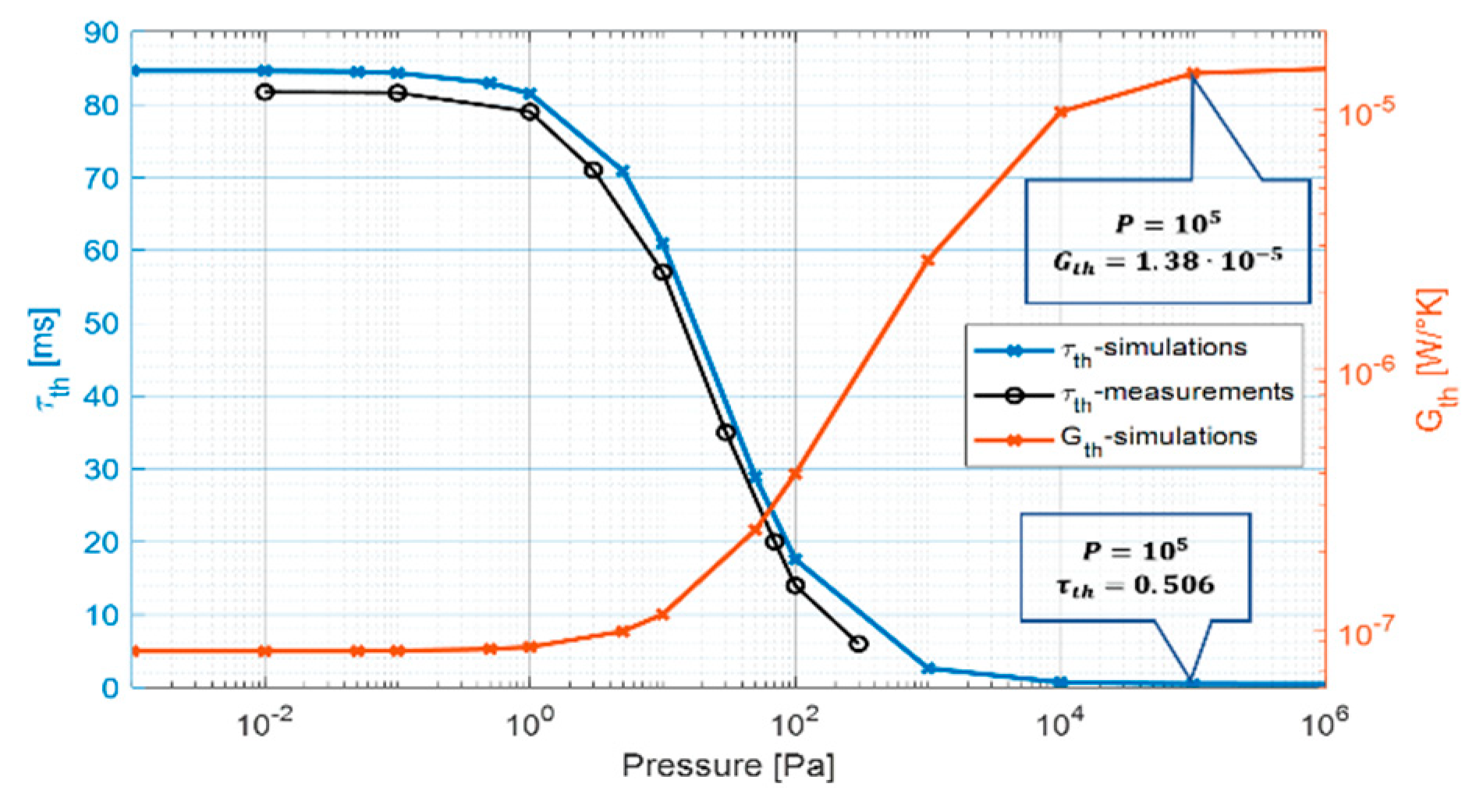
After receiving the thermal conductance by the gas and solids from the simulation results, the total thermal conductance of the system, including radiation, can be evaluated by solving Equations (6, 8) iteratively. The results are shown in
Figure 5.
The thermal conductance changed from at low pressure to at atmospheric pressure . It should be noted that at a high vacuum where heat is transferred by conduction through the holding arms, the analytically modeled and the simulated are in good agreement. At atmospheric pressure, the main heat transfer mechanism is governed by the gas. By applying the of the gas at atmospheric pressure, the distance to the top packaging filter, and the total area of the 16 suspended, micromachined plates, the analytically evaluated agrees with the simulated one. The thermal time constant changed from at low pressure to at atmospheric pressure .


