
A New Symmetric and Asymmetric Multilevel Inverter Circuit with Reduced Number of Components †


Department of Electrical and Electronics Engineering, Sri Sivasubramaniya Nadar College of Engineering, Chennai 603 110, India
†
Presented at the International Conference on Innovative Research in Renewable Energy Technologies, West Bengal, India, 16–17 March 2022.
Mater. Proc. 2022, 10(1), 5; https://0-doi-org.brum.beds.ac.uk/10.3390/materproc2022010005
Published: 22 July 2022
(This article belongs to the Proceedings of The 2nd International Conference on Innovative Research in Renewable Energy Technologies (IRRET 2022))
Abstract
:Multilevel inverters (MLIs) have emerged as a feasible option for medium-voltage energy conversion applications with excellent power quality. These inverters have exhibited different advantages over the two-level inverters due to the development of various modulation schemes. In recent years, they have received a lot of attention for a variety of industrial applications, including adjustable speed drives, renewable energy systems, electric vehicles and uninterruptible power supply. The main aim of this paper is to propose a new symmetric- and asymmetric-type multilevel inverter circuit with a reduced number of circuit components. The proposed circuit consists of three DC voltage sources and nine power electronic switches. The proposed topology creates a staircase-type 7-level output voltage waveform under a symmetric condition and a 15-level output voltage waveform under an asymmetric condition, with fewer components and low total harmonic distortion, without using an active filter circuit. A comprehensive comparative analysis is presented to illustrate the advantage of the proposed inverter circuit. The performance of the proposed MLI is verified through many simulation studies in MATLAB/Simulink. Furthermore, to highlight the merits and superiorities of the suggested MLI, a full comparison is performed with the best performance of the existing MLI topologies.
1. Introduction
Nowadays, multilevel inverters (MLIs) are gaining more and more popularity and extremely high-quality voltage source power converters, which help to interconnect the DC system with an AC system [1]. MLIs can generate a stepped medium voltage waveform using diodes, DC supplies and power switches while operating at a low switching frequency. The most prominent advantages of MLIs are low total harmonic distortions (THD), low dv/dt stress on the power electronic switches, satisfactory power quality, low ripple factor, good electromagnetic compatibility, high voltage operation capability, high power density, great efficiency and easy controllability [2,3]. Because of these advantages, MLIs are an excellent fit and best suited for various high-voltage and high-power conversion systems, including variable-speed motor drives, flexible AC transmission systems (FACTS), renewable energy and electric vehicles [4]. MLIs are more effective than ordinary inverters for medium and high-voltage applications because they use a larger number of power semiconductor switches and DC voltage sources, lowering the power switch rating. Neutral point clamped (NPC), flying capacitor (FC) and cascaded H-Bridge (CHB) are the three different types of standard MLIs [5,6]. Due to the employment of various de-vices in their circuits, these MLIs have their own prices and complications. The neutral point balance is a difficulty with NPCMLIs, and increase in the number of diodes in higher voltage levels is their main drawback. It is assumed that during the passage of the equivalent voltage across the DC link capacitors, each active switching device will experience high voltage stress, which will be clamped to the voltage of each capacitor via diode clamping [7]. The blocking voltage is shared in a real application by serially connecting the clamping diodes. The diode reverse recovery of these clamping diodes is a serious concern with the design in high-voltage applications when using the DCMLI with PWM. A high number of flying capacitors are used in FCMLIs, and the voltage balance of these capacitors is difficult. The inrush current that goes through the capacitor and several switches is a major source of worry in FCMLIs. When compared to a NPCMLI, the voltage synthesis in the FCMLI is more flexible. When there are more than five levels, the voltage balance problem across the FCs can be solved by choosing the right switching combination. The reactive and active power can be managed with this design; however, the usage of multiple FCs makes the system complex and expensive. Furthermore, in real power transmission, the switching losses are substantial in such configurations [8]. Unlike FC and NPC, CHB uses a cascaded and modular inverter structure [9]. As the number of power switches grows, the number of driving circuits grows as well. As a result, an increase in the size, cost and complexity of the MLIs is unavoidable, lowering the inverter’s efficiency and reliability. To put it another way, there is a tradeoff between the number of power components and the inverter’s cost, complexity and efficiency. As a result, despite CHB’s excellent scalability, its vast number of power switches is a major drawback, resulting in higher costs, lower reliability and lower efficiency [10]. The key challenge that all researchers in this subject confront is determining the most optimum MLI topology to attain higher performance with the fewest number of components and achieve the required higher levels.
A new inverter structure consisting of cascading basic units and an H-bridge is pro-posed in Ref. [1]. The conduction losses are increased in this inverter structure due to the large number of bidirectional switches. The total peak inverse voltage (PIV) of the switches is very high, and as a result, this inverter is expensive and unsuitable for ap-plications requiring high voltage. Ref. [2] introduces a new multilevel inverter with a higher number of switches than the CHB converter. It suggests a unique configuration made up of a sequence of modules. Two DC sources and four power electronic switches are included in each module. In comparison to the CHB-based inverter, this topology has various advantages, such as simplicity, adaptability and redundancy. However, their peak inverse voltages (PIVs) are, nevertheless, higher than those of the proposed structure. Other simple modular topology presented in Ref. [3] consists of unidirectional switches and fewer DC voltage sources. However, such topology includes switches with different voltage ratings and a large number of circuit components, all of which add to the complexity of the inverter structure. The MLI structure provided in Ref. [4] attempted to reduce the number of components while improving several elements, such as efficiency and cost. The reliability of these structures, on the other hand, was not taken into account as a critical factor. The switches have varying voltage ratings, and the voltage-balancing circuit’s structure is complicated. In addition, high TSV across the switches is the main disadvantage of this inverter, resulting in low reliability. The inverter circuits in Refs. [5,6,7,8] necessitate a greater number of switches, many of which are bidirectional, as well as a significant number of conducting switches. As a result of their poorer efficiency, they have been limited in their use in high-power energy conversion systems.
The paper is organized as follows. Section 2 discusses the proposed inverter structure and functioning, while Section 3 presents the comprehensive comparative analysis of the proposed inverter structure with other recent topologies. In Section 4, the simulation findings are analyzed, and in Section 5, the conclusions are presented.
2. Proposed 51-Level Inverter
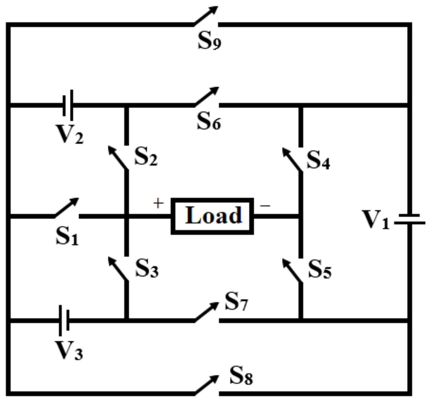
The proposed symmetric- and asymmetric-type inverter structure is shown in Figure 1. The proposed inverter consists of three DC voltage sources and nine power semiconductor switches. The proposed inverter circuit can operate at both equal and unequal magnitude of DC voltage sources. With equal DC voltage magnitude, i.e., V1 = V2 = V3 = Vdc, the proposed inverter circuit can generate seven-level output voltage with three positive levels, three negative levels and a zero level. With unequal DC voltage magnitude, i.e., V1 = Vdc; V2 = 2Vdc; V3 = 4Vdc, the proposed inverter circuit can generate 15-level output voltage with 7 positive levels, 7 negative levels and a zero level. Figure 2 shows some of the sample positive and negative output levels obtained for the proposed inverter circuit. In order to avoid short circuit, the following switching combinations should not be turned ON simultaneously: (S1, S2), (S1, S3), (S2, S3), (S4, S5), (S6, S9) and (S7, S8).
The maximum number of switches turned ON to create any output level is equal to three switches, which is a very low number as compared with other topologies. The maximum magnitude of the obtained output voltage is given by Vout,max = V1 + V2 + V3. The switching tables for 7-level and 15-level inverter operations are given in Table 1 and Table 2, respectively. It is noted that the switch S7 is turned ON during positive cycle, and S6 is turned ON during negative cycle during 7-level inverter operation. During 15-level inverter operation, the switches S6 and S9 are turned OFF during positive cycle, and the switches S7 and S8 are turned OFF during negative cycle. The zero level can be obtained by turning ON the switches (S3, S5, S7) or (S2, S4, S6).
3. Comparison Study
In this section, different symmetric-type 7-level inverter and asymmetric 15-level inverter topologies are compared based on the required number of switching devices, DC voltage sources, ON-state switches and total standing voltage (TSV) value of the switches. The comparative results of the proposed MLI with the other latest inverter circuits are presented in Table 3. The MLI circuit presented in Refs. [1,2,6] contains a half-bridge unit to obtain the negative levels at the output. The MLI circuits presented in Refs. [7,8] have the capability to attain the negative output levels without adding a half-bridge unit. The topologies presented in Refs. [1,2,6] require ten switches to create seven output levels during symmetric operation and fifteen output levels during asymmetric operation. The TSV value for the proposed inverter during 7-level and 15-level operation is 17Vdc and 40Vdc, respectively, which is also lower than the other topologies presented in the literature. The TSV value for the 15-level inverter topology presented in Refs. [2,6] requires 50Vdc. For a 15-level operation, the TSV value is 48Vdc, and it is 54Vdc for the inverter presented in Refs. [8] and [7], respectively. It is notable that the cost and size of the MLI topologies increase with the increase in the number of MLI circuit components and increase in the TSV value. In this regard, the cost and size of the proposed MLI circuit are very minimum as compared with the other presented topologies.
4. Simulation Results
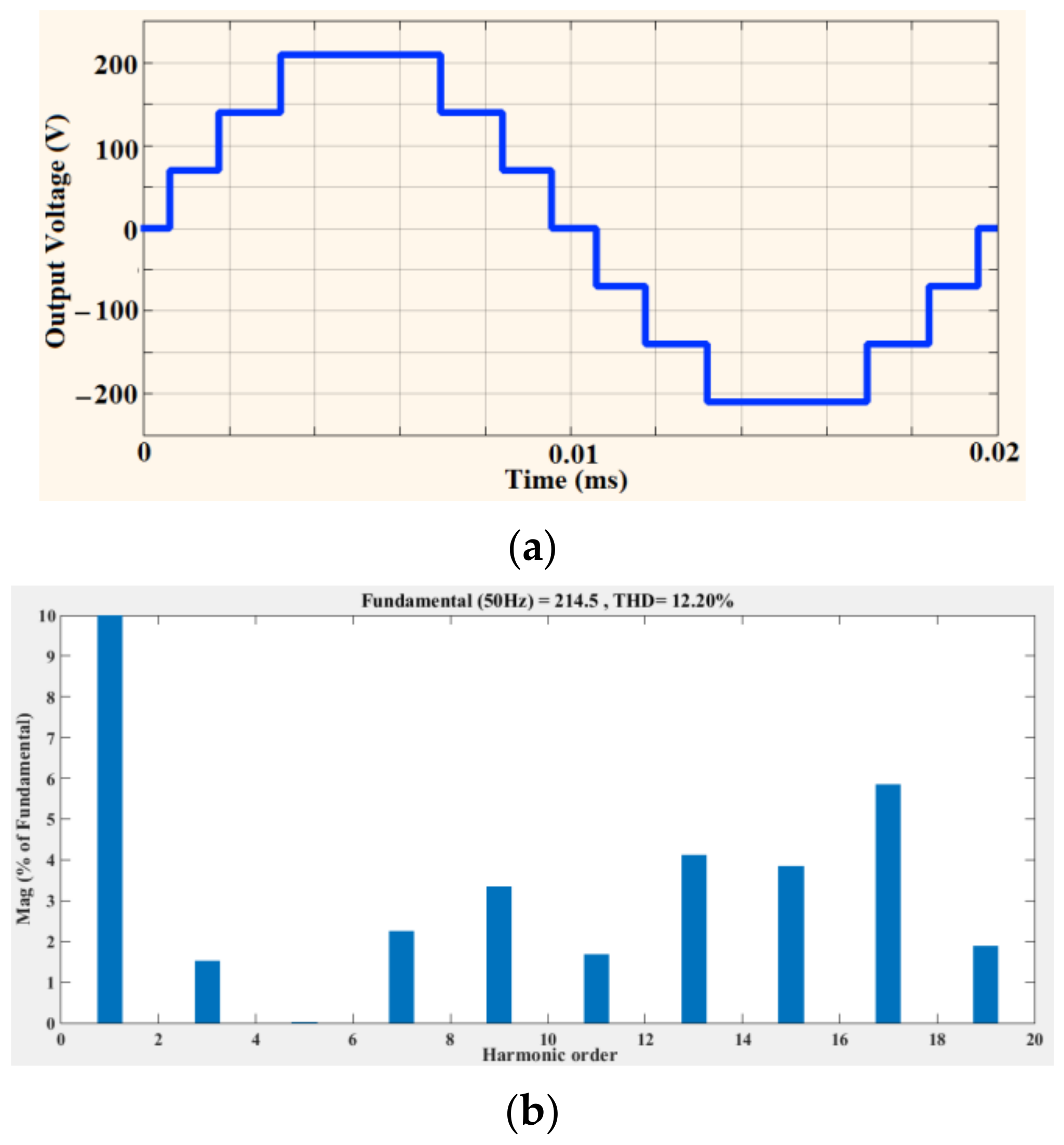
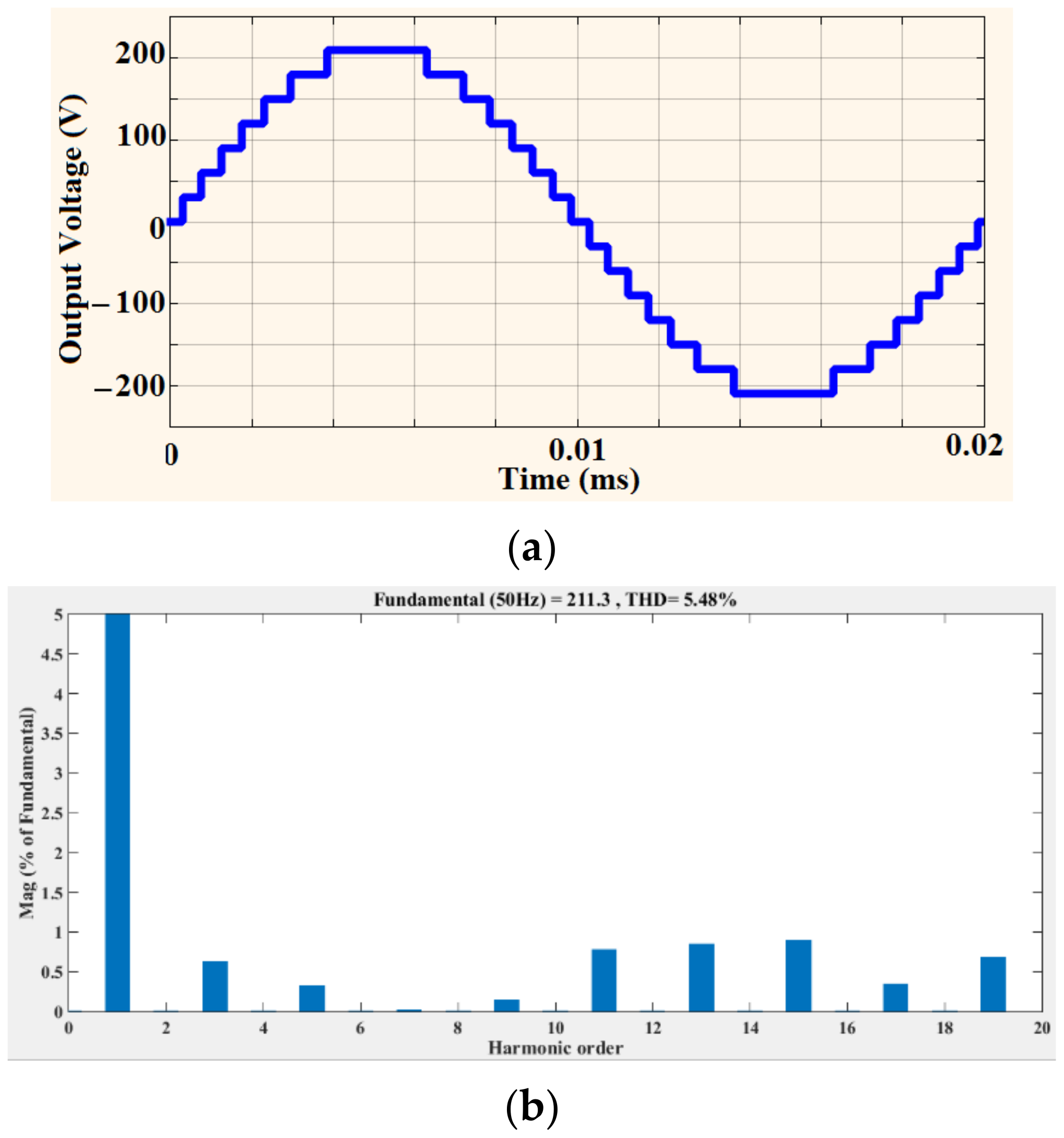
The simulation analysis of the proposed MLI circuit is carried out using Simulink/MATLAB software. During the seven-level symmetrical inverter operation, the DC voltage magnitudes are selected as V1 = V2 = V3 = Vdc = 70 V, and hence, the maximum voltage magnitude obtained is 210 V. During the 15-level asymmetrical inverter operation, the DC voltage magnitudes are selected as V1 = Vdc = 30 V, V2 = 2Vdc = 60 V and V3 = 4Vdc = 120 V, and hence, the maximum voltage magnitude obtained is 210 V. The load parameters considered for the simulation are R = 50 Ω and L = 100 mH.
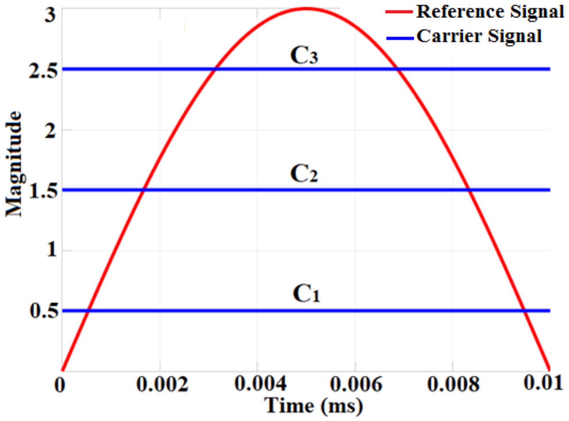
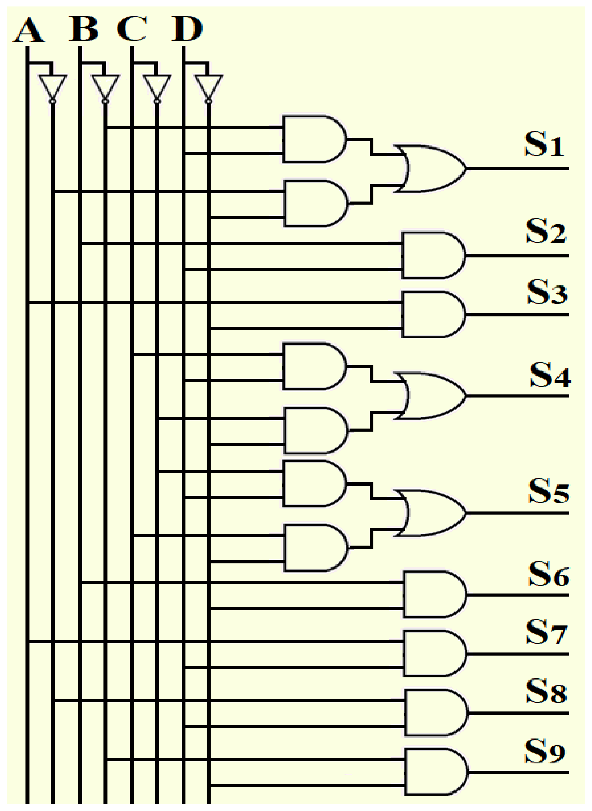
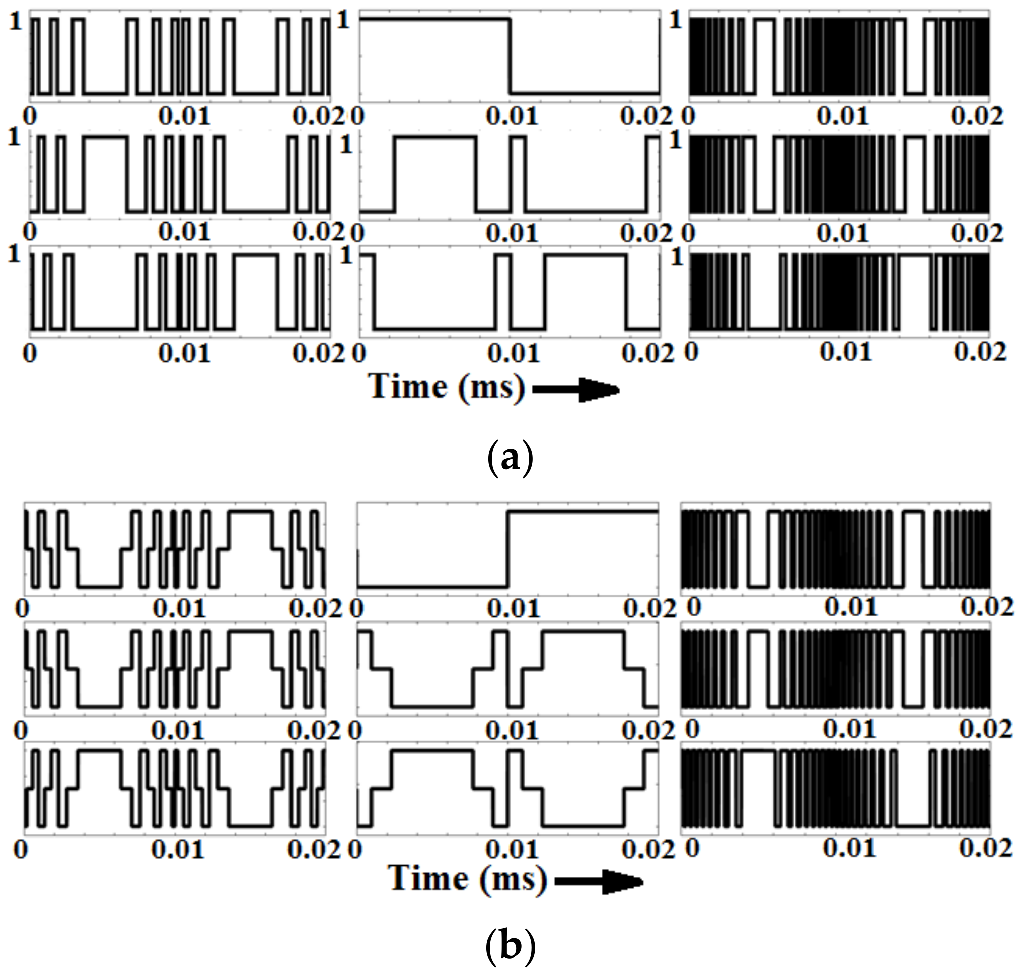
Different modulation approaches have been devised to control the power flow in the MLIs. Some of the common modulation methods described in the literature include phase shifted carrier pulse width modulation (PS-PWM), pulse width amplitude modulation (PWAM) and space vector pulse width modulation (SVPWM). PS-PWAM achieves excellent and optimal semiconductor switching but at the expense of flexibility, and it sacrifices modularity. In this paper, a carrier-based digital logic pulse width modulation method is introduced in which (N-1)/2 carrier signals are compared with a reference signal to generate (N-3)/2 intermediate signals, where N is the number of output levels. Using these intermediate signals, the required switching signals for the power semiconductor devices are generated with the implementation of the digital logic circuit using a fundamental AND, OR and NOT gates. Therefore, 3- and 7-carrier signals are compared with a reference sinusoidal signal to generate 2-intermediate signals (A and B) and 3-intermediate signals (A, B and C) for 7-level and 15-level inverter operations, respectively. The amplitude of each carrier signal is determined using the formula
where m is the number of output voltage levels, and Vm is the magnitude of the reference sinusoidal signal.
Figure 3 shows the generation of an intermediate signal for a 7-level inverter by comparing three carrier signals with a reference sinusoidal signal. Figure 4 shows the implementation of the digital logic circuit to obtain the required switching pulses for a 15-level inverter.
Figure 5a,b show the voltage stress across each switch of the proposed MLI circuit during symmetric and asymmetric operation, respectively. The voltage stress across the switch S1 is (V2) V, and it is (V2 + V3)V for the switches S2 and S3. For switches S4 and S5, the voltage stress is equal to V1 V, and the maximum voltage stress of (V1 + V2 + V3)V is obtained across the switches S6 and S7, respectively. The voltage stress across the switches S8 and S9 is equal to (V1 + V3)V. Hence, the total standing voltage (TSV) across the switches of the proposed inverter circuit is equal to (6V1 + 5V2 + 6V3)V.
The output voltage waveform and its total harmonic distortion (THD) for 7-level and 15-level inverters are shown in Figure 6 and Figure 7, respectively. As anticipated, the output voltage is of the stepped waveform, closely, with minimum THD of 12.20% and 5.48%, respectively, for 7-level and 15-level inverters.
5. Conclusions
This paper presents a new symmetric- and asymmetric-type inverter module that reduces the number of switches and DC voltage sources. The proposed inverter circuit has quite a few distinctions, including the reduced switch count, less blocking voltage of the power semiconductor switches and the ability to create negative output levels without any supplementary circuit. The merits of the proposed inverter circuit are confirmed through the latest comparable MLI topologies. In addition, the proposed inverter offers fewer switching losses, improved efficiency and better output quality. At last, the simulation results of the 7-level and 15-level inverter obtained using Matlab/Simulink software are presented. The proposed MLI is more suitable for medium power and high-voltage industrial applications with renewable energy sources, such as solar and fuel cells.
Funding
This research received no external funding.
Institutional Review Board Statement
Not applicable.
Informed Consent Statement
Not applicable.
Data Availability Statement
Not applicable.
Conflicts of Interest
The authors declare no conflict of interest.
References
- Babaei, E.; Hosseini, S.H. New cascaded multilevel inverter topology with minimum number of switches. Energy Convers. Manag. 2009, 50, 2761–2767. [Google Scholar] [CrossRef]
- Toupchi Khosroshahi, M. Crisscross cascade multilevel inverter with reduction in number of components. IET Power Electron. 2014, 7, 2914–2924. [Google Scholar] [CrossRef]
- Thiyagarajan, V.; Somasundaram, P. Simulation of New Symmetric and Asymmetric Multilevel Inverter Topology with Reduced Number of Switches. In Proceedings of the 4th International Conference on Electrical Energy Systems (ICEES), Chennai, India, 7–9 February 2018. [Google Scholar]
- Thiyagarajan, V. New Symmetric Extendable Type Multilevel Inverter Topology with Reduced Switch Count. In Proceedings of the 5th International Conference on Electrical Energy Systems (ICEES), Chennai, India, 21–22 February 2019. [Google Scholar]
- Poorfakhraei, A.; Narimani, M.; Emadi, A. A Review of Multilevel Inverter Topologies in Electric Vehicles: Current Status and Future Trends. IEEE Open J. Power Electron. 2021, 2, 155–170. [Google Scholar] [CrossRef]
- Venkatraman, T.; Periasamy, S. Multilevel Inverter Topology with Modified Pulse Width Modulation and Reduced Switch Count. Acta Polytech. Hung. 2018, 15, 141–167. [Google Scholar]
- Aparna, P.; Sanjay, B. Novel Basic Block of Multilevel Inverter Using Reduced Number of On-State Switches and Cascaded Circuit Topology. Adv. Electr. Eng. 2017, 2017, 5640926. [Google Scholar] [CrossRef] [Green Version]
- Khenar, M.; Taghvaie, A.; Adabi, J.; Rezanejad, M. Multi-level inverter with combined T-type and cross-connected modules. IET Power Electron. 2018, 11, 1407–1415. [Google Scholar] [CrossRef]
- Thiyagarajan, V.; Somasundaram, P. New Asymmetric 21-Level Inverter with Reduced Number of Switches. J. Eng. Res. 2019, 16, 18–27. [Google Scholar] [CrossRef] [Green Version]
- Anitha, M.; Somasundaram, P.; Thiyagarajan, V. Photovoltaic based New Multilevel Inverter Topology with Minimum Number of Switching Components. J. Electr. Eng. 2019, 19, 10. [Google Scholar]
Figure 1.
Proposed inverter topology.

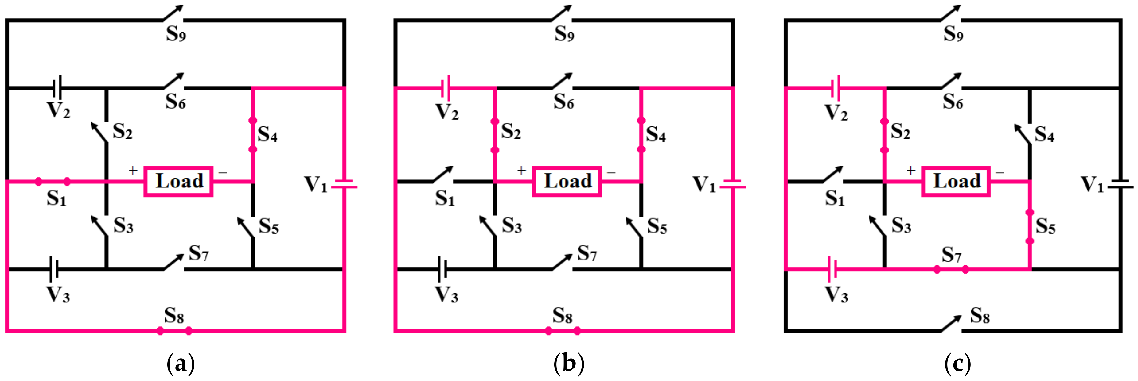
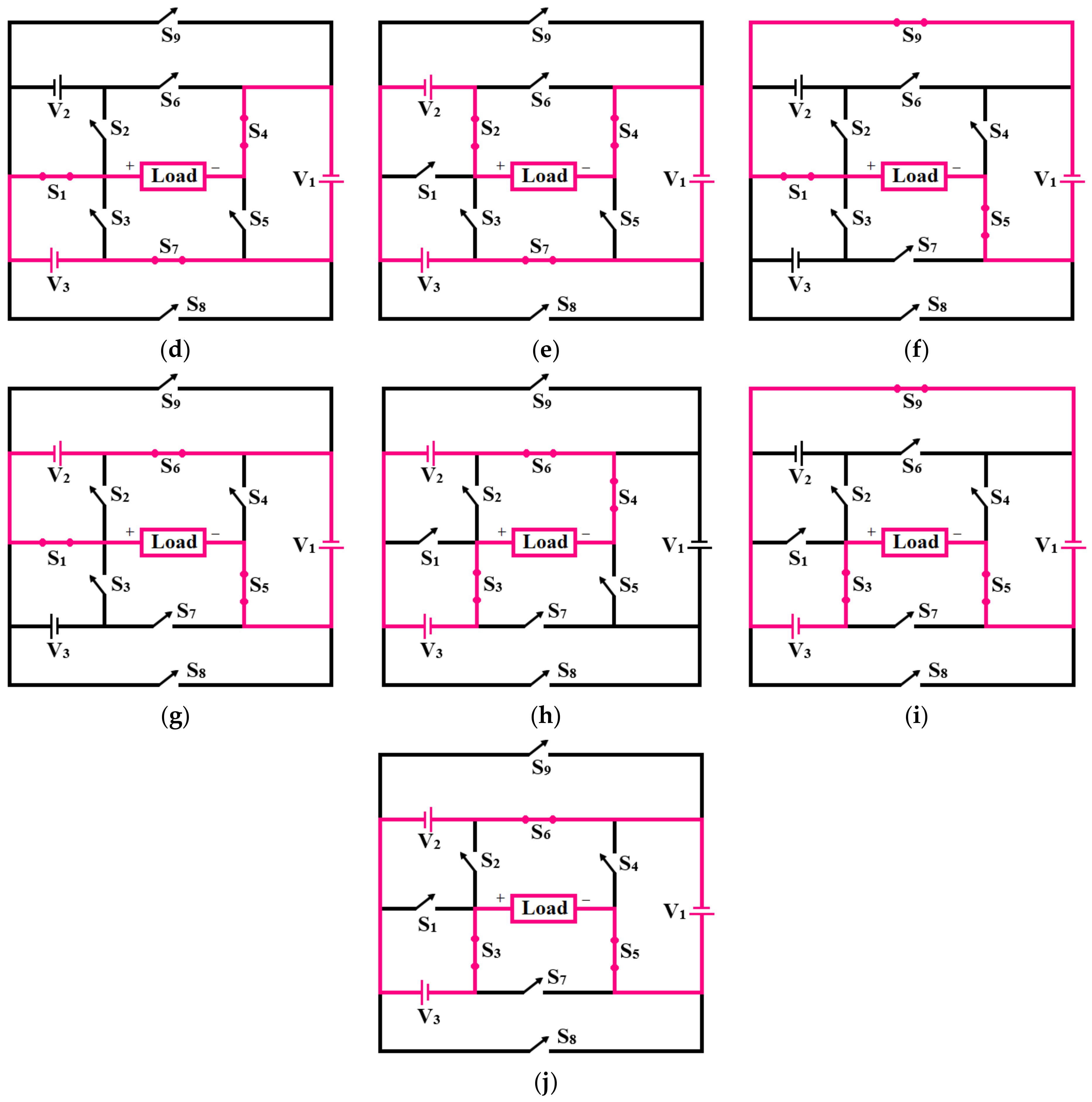
Figure 2.
Various output voltage levels. (a) V1; (b) V1 + V2; (c) V2 + V3; (d) V1 + V3; (e) V1 + V2 + V3; (f) −V1; (g) −V1 − V3; (h) −V2 − V3; (i) −V1− V3; (j) −V1 − V2 − V3.
Figure 2.
Various output voltage levels. (a) V1; (b) V1 + V2; (c) V2 + V3; (d) V1 + V3; (e) V1 + V2 + V3; (f) −V1; (g) −V1 − V3; (h) −V2 − V3; (i) −V1− V3; (j) −V1 − V2 − V3.


Figure 3.
Carrier Pulse with Sinusoidal Reference Waveform for a 7-level inverter.

Figure 4.
Implementation of Digital Logic Gates Circuit—15-level.

Figure 5.
Voltage stress across the switches (a) 7-level (b) 15-level.

Figure 6.
Simulation results with R = 0 Ω and L = 200 mH. (a) Output waveform; (b) THD.

Figure 7.
Simulation results with R = 15 Ω and L = 150 mH. (a) Output waveform; (b) THD.


Table 1.
Switching Table—7-Level.
| Level | Positive Cycle | Negative Cycle | ||
|---|---|---|---|---|
| Voltage Sources | Switches | Voltage Sources | Switches | |
| 0 | - | S3, S5, S7 | - | S2, S4, S6 |
| 1 | V3 | S1, S5, S7 | V1 | S1, S5, S9 |
| 2 | V2 + V3 | S2, S5, S7 | V1 + V2 | S1, S5, S6 |
| 3 | V1 + V2 + V3 | S2, S4, S7 | V1 + V2 + V3 | S3, S5, S6 |
Table 2.
Switching Table—15-Level.
| Level | Positive Cycle | Negative Cycle | ||
|---|---|---|---|---|
| Voltage Sources | Switches | Voltage Sources | Switches | |
| 0 | - | S3, S5, S7 | - | S2, S4, S6 |
| 1 | V1 | S1, S4, S8 | V1 | S1, S5, S9 |
| 2 | V2 | S2, S5, S8 | V2 | S1, S4, S6 |
| 3 | V1 + V2 | S2, S4, S8 | V1 + V2 | S1, S5, S6 |
| 4 | V3 | S1, S5, S7 | V3 | S3, S4, S9 |
| 5 | V1 + V3 | S1, S4, S7 | V1 + V3 | S3, S5, S9 |
| 6 | V2 + V3 | S2, S5, S7 | V2 + V3 | S3, S4, S6 |
| 7 | V1 + V2 + V3 | S2, S4, S7 | V1 + V2 + V3 | S3, S5, S6 |
Table 3.
Comparative Analysis.
| Topology | Negative Level | No. of Sources | No. of Switches | ON-State Switches | TSV | Level |
|---|---|---|---|---|---|---|
| [1] | H-Bridge | 3 | 10 | 5 | 18Vdc | 7-Level |
| [2] | H-Bridge | 3 | 10 | 5 | 22Vdc | 7-Level |
| [6] | H-Bridge | 3 | 10 | 4 | 21Vdc | 7-Level |
| [7] | Inherent | 3 | 12 | 5 | 24Vdc | 7-Level |
| [8] | Inherent | 3 | 14 | 5 | 20Vdc | 7-Level |
| Proposed | Inherent | 3 | 9 | 3 | 17Vdc | 7-Level |
| [1] | H-Bridge | 3 | 10 | 5 | 42Vdc | 15-Level |
| [2] | H-Bridge | 3 | 10 | 5 | 50Vdc | 15-Level |
| [6] | H-Bridge | 3 | 10 | 4 | 50Vdc | 15-Level |
| [7] | Inherent | 4 | 12 | 6 | 54Vdc | 15-Level |
| [8] | Inherent | 3 | 12 | 6 | 48Vdc | 15-Level |
| Proposed | Inherent | 3 | 9 | 5 | 40Vdc | 15-Level |
Publisher’s Note: MDPI stays neutral with regard to jurisdictional claims in published maps and institutional affiliations. |
© 2022 by the author. Licensee MDPI, Basel, Switzerland. This article is an open access article distributed under the terms and conditions of the Creative Commons Attribution (CC BY) license (https://creativecommons.org/licenses/by/4.0/).
Share and Cite
MDPI and ACS Style
Thiyagarajan, V. A New Symmetric and Asymmetric Multilevel Inverter Circuit with Reduced Number of Components. Mater. Proc. 2022, 10, 5. https://0-doi-org.brum.beds.ac.uk/10.3390/materproc2022010005
AMA Style
Thiyagarajan V. A New Symmetric and Asymmetric Multilevel Inverter Circuit with Reduced Number of Components. Materials Proceedings. 2022; 10(1):5. https://0-doi-org.brum.beds.ac.uk/10.3390/materproc2022010005
Chicago/Turabian StyleThiyagarajan, Venkatraman. 2022. "A New Symmetric and Asymmetric Multilevel Inverter Circuit with Reduced Number of Components" Materials Proceedings 10, no. 1: 5. https://0-doi-org.brum.beds.ac.uk/10.3390/materproc2022010005