Article

Design, Analysis and Experimental Verification of the Self-Resonant Inverter for Induction Heating Crucible Melting Furnace Based on IGBTs Connected in Parallel

1
School of Engineering, Warwick University, Coventry CV4 7AL, UK
2
School of Engineering, Computing and Mathematics, Oxford Brookes University, Oxford OX3 0BP, UK
*
Author to whom correspondence should be addressed.
Submission received: 13 July 2021 / Revised: 24 September 2021 / Accepted: 28 September 2021 / Published: 11 October 2021
(This article belongs to the Topic Application of Innovative Power Electronic Technologies)

Abstract

:
The object of this research was a self-resonated inverter, based on paralleled Insulated-Gate Bipolar Transistors (IGBTs), for high-frequency induction heating equipment, operating in a wide range of output powers, applicable for research and industrial purposes. For the nominal installed capacity for these types of invertors to be improved, the presented inverter with a modified circuit comprising IGBT transistors connected in parallel was explored. The suggested topology required several engineering problems to be solved: minimisation of the current mismatch amongst the paralleled transistors; a precise analysis of the dynamic and static transistors’ parameters; determination of the derating and mismatch factors necessary for a reliable design; experimental verification confirming the applicability of the suggested topology in the investigated inverter. This paper presents the design and analysis of IGBT transistors based on datasheet parameters and mathematical apparatus application. The expected current mismatch and the necessary derating factor, based on the expected mismatch in transistor parameters in a production lot, were determined. The suggested design was experimentally tested and investigated using a self-resonant inverter model in a melting crucible induction laboratory furnace.

1. Introduction

This paper aimed to design, analyse, prototype, and experimentally test a self-resonant inverter for crucible inductance furnaces to verify the suggested circuit based on IGBTs connected in parallel. For this purpose, a methodology for analysing the transistors’ characteristics and the expected mismatch in a production lot was suggested and implied as part of the design procedure. It was based on trend analysis of the transistors’ datasheets, digitalising the graphical data and deriving precise polynomial equations. Such a study aimed to compensate for the lack of data on the mismatch of IGBT parameters. In this sense, the presented research’s novelty consisted of modifying a well-known circuit, which was analysed with a novel methodology focused on paralleled transistors, giving the expected current mismatch and the necessary derating factor.
As a highly efficient and fast method, induction heating is applicable for numerous technological processes of heating, melting, hardening, etc. The investigated crucible furnaces are used for metal melting, such as gold, steel and copper, applied in different industries—jewellery, steel production, etc. The theoretical basis of induction systems has been described in multiple well-established literature sources [1,2,3,4,5,6], giving fundamental knowledge for the system inductor-workpiece.
A popular method for induction heating analysis is modelling and simulation with the Finite Element Method (FEM), which depicts the system’s electromagnetic field inductor-workpiece. The system’s thermal and electrical parameters can be analysed, as well as the required parameters of the high-frequency electronic converter to be predicted on the simulation level. Using FEM, in [7,8], an induction heating process with a moving inductor or workpiece was presented. Such systems require considerable power to be transferred for a short time for the necessary temperature to be reached at the required time. For this purpose, significant currents through the inductor, for example, 450–890 A at 36 kHz [8], must be supplied from the induction heating inverter. The optimisation of the inductor-workpiece system gave positive results [9] for the magnetic coupling but did not minimise the current provided, presented in most FEM models in the range of 106–108 A/m2.
According to the research published in [10], the induction heating process with spray cooling, realised by the presented experimental equipment, can continue for a relatively long time at about 30 min. The required inductor current exceeded 400 A. The provided experiments were used for FEM model calibration. A similar study [11], based on the induction heating and FEM modelling analysis, showed a process established at a relatively low frequency of 3 kHz and 544.5 A current through the inductor. Higher frequencies, up to 20 kHz, can be applied for magnetic and nonmagnetic workpieces [12]. The presented experimental verification in [12] was completed with a low-voltage inductor, rated at 47.1 V, which gave a maximum current of 1063 A. In addition, the used capacitor tank at the resonant tank was rated at 15.41 µF or 55.7 µF, which gave a resonant frequency of between 10 kHz and 20 kHz.
Studies focused on the influence of the workpiece characteristics over the heating process [13,14,15] have shown that the inductor geometry characteristics have a critical impact on the electromagnetic field shape and must be considered with the specific workpiece. This phenomenon has the potential to influence the inverter characteristics influenced by the inductor length and its inductivity and, hence, the resonance frequency with the necessary capacitance tank, as well as the inverter’s output current at a given power, which requires additional study.
Another group of recently published papers [16,17,18], focusing on the development and application of new materials, showed the induction heating application for materials’ laboratory production and further investigation. The technological parameters required variations in broad ranges in output power of 10–200 kW, inductor currents up to thousands of amps, low or high inductor voltages and resonant frequencies up to 300 kHz. The exact requirements can be stated for flat-inductor systems [19] and melting induction furnaces [20]. They clearly show that with respect to the industrial equipment with specific parameters, the laboratory induction heating must be much more flexible, which would ensure its application for different laboratory tests and studies. According to these requirements, self-oscillating inverters for induction heating are good candidates for laboratory equipment as a simple structure that is highly reliability and naturally operating with inherent Zero Voltage Switching (ZVS) modulation, which gives low switching losses. In [21,22,23], a self-oscillating inverter with a parallel resonant tank operating at a relatively low power of 300 W was proposed. The research showed the advantages of implementing a Current Source Parallel Resonant Push-Pull Inverter (CSPRPI) and the possibilities of achieving ZVS with low switching losses. A similar topology based on a half-bridge but a series resonant tank was also proven to have a stable operation at ZVS [24]. Furthermore, the same source proved that these classes of converters can be controlled with a simple phase-locked loop based on a variable duty cycle.
A converter structure with proven application in induction heating, giving high power density and the ability to operate with soft-switching, is the full-bridge circuit with a parallel or series resonant tank, based on different modulation techniques, such as Phase-Shift Modulation (PSM), Pulse-Frequency Modulation (PFM), Pulse-Density Modulation (PDM) and Asymmetrical Duty-Cycle (ADC) [25,26,27,28,29,30,31]. These types of modulation offer flexible control over the wide range of output powers [25]. These inverters applied for induction heating can have a good match with a Power Factor Correction (PFC) stage [26]. An additional characteristic of the PSM is the ability of the ZVS to be achieved for the required power range under regulation with variable switching frequency [27]. It has been shown that the use of variable switching has a better efficiency than a fixed switching frequency. Despite the modulation technique, the problem with the transient overvoltages and electromagnetic interference (EMI) due to the transistor switching is mitigated with snubbers.
In contrast to the self-oscillating inverters [21,22,23], one of their advantages is usually based on snubber-less power stage circuits for the full-bridge PSM topology, and different types of passive snubbers such as C, RC, and RCD can be used. Their selection and design depend on the modulation technique and the match between the used IGBTs and the resonant tank parameters [28,29]. In the same class, transformer-based converters are the LLC resonant inverters. A powerful inverter of this type, rated at 25 kW with a fixed frequency of 25 kHz, is presented in [30]. Transformer-less topologies based on a full-bridge can be realised as matrix converters, whose topology requires bi-directional switches [31]. Although these converters have significant advantages, a comparative analysis shows that the self-resonant converters are based on a more straightforward structure, giving a budget-friendly induction heating system, with low EMI, without snubber circuits and low losses.
Another group of papers focused on induction heating devices for cooking [32,33,34,35,36], which usually have flat inductors and an installed power in the range of 1.5–2.8 kW. According to their shapes and materials, an important issue is the magnetic coupling between the inductor and the loads, i.e., pan, pot and wok [32,33]. The other parts of the control system: sensors, feedbacks, filters, etc., are also well investigated from the cooking-intended induction heaters [34,35,36]. The reported efficiency for cooking induction heating converters is over 95%, which can be expected as a parameter for a powerful induction heating crucible system.
The provided literature review concludes that the self-oscillating resonant converters have the simplest circuit, offering a robust and budget-friendly solution. Currently, they are applied for relatively low power in the range of 300–800 W as laboratory equipment, using cylindrical inductors for heating magnetic elements [37,38]. It can be suggested that their application can be extended to more considerable powers, over 30 kW, and a frequency range of 25–35 kHz, giving an application for fast-melting crucible inductance furnaces [39]. Such a power would require a power stage based on IGBT transistors connected in parallel to be designed and implemented. Numerous papers [40,41,42,43,44,45,46,47] present research mainly focused on IGBTs. Current equalisation with improved gate drive control implemented with Digital Signal Processors (DSPs) and precise current measurements is given in [40,41]. Strategies based on active driver circuits and current cross-reference control techniques were proposed in [42], including for Silicon Carbide (SiC) MOSFETs [43,44].
Nowadays, Revers Conducting IGBTs (RC-IGBTs), specialised for resonant inverters, i.e., applicable for induction heating systems, are offered by manufacturers [45,46,47,48]. According to the presented applications [45], the analysis of the transistors’ technology and their implementation in the induction inverters [47] justifies the suggestion that paralleled RC-IGBT can operate with a good current sharing and, hence, low current mismatch. The experimental data presented with oscillograms showed inverters’ soft-switching operation [45,47,48,49,50] in the induction heating resonant inverters. Furthermore, the assembling procedure applied for half-bridge resonant inverters [46] implies that current equalisation for the self-resonant induction converters based on paralleled IGBTs can be easily achievable. All of the stated suggestions require additional analytical and experimental research as such has not been found in the literature. Some statistical information about the parameters’ dispersion of IGBT modules is given in [50], but no analysis or experimental data have been found for discrete transistors.
As a conclusion from the presented literature review: the self-resonant converters for induction heating [21,22,23,24] are an applicable technology giving reliable and budget-friendly solutions; induction heating inverters, with an installed power higher than 10–15 kW for industrial and laboratory research purposes [29,30,31], can be constructed by IGBT transistors connected in parallel, but the literature presenting such applications specifically for self-resonated inverters is insufficient; although the paralleling of transistors is an object of significant research [40,41,42,43,44], the application of this topology in the self-resonance architectures requires additional investigation. In general, from the literature, it is clear that the topology of self-resonant inverters for induction crucible melting furnaces has the potential to reach higher powers with paralleled transistors. However, the undesirable phenomena caused by transistors’ parameters mismatches are not well described in the literature specifically for this application. Furthermore, the parallel operation in the resonant inverters can cause problems such as uneven current allocation, operation outside the ZVS region and major malfunction.
Based on the presented literature findings, the primary purpose of the suggested research was to experimentally show the possibility of resonant inverters with paralleled IGBTs operating with improved characteristics. For this purpose, a methodology for the analysis of transistors’ characteristics was developed, giving a precise estimation of the paralleling IGBTs abilities. The presented approach estimated the derating factors and the expected current share through digitalising the graphical data and conducting a thorough analysis.
The paper is organised as follows: Section 2 shows an analysis of the modified self-resonated inverter based on the suggested methodology for analysis of the transistors connected in parallel; Section 3 shows an experimental verification; the conclusions are presented in Section 4.

2. Analysis of the Investigated Inverter, Based on RC-IGBTs in Parallel

The self-resonated converter is shown in Figure 1. The object of this research was the power stage of the inverter, which is part of the entire system presented with a block diagram. The further analysis and the experimental model presented in Section 3 were completed with discrete RC-IGBTs. In this circuit, it is necessary for the transistors’ emitters to be connected at a common point (GND); off-the-shelf half-bridge IGBT modules would not be suitable. Analysing the IGBTs currently available on the market, the targeted power for the designed crucible melting induction system in a range of 20–30 kW, with a potential to reach 50 kW, could be achieved with 3 to 8 high and low side transistors connected in parallel. Such a circuit applies the necessity of a precise analysis of the IGBTs parameters to be undertaken due to the specific parasitic elements that the discrete packages, usually TO-247, TO263, etc., and their modification typically have. The gate drive circuits are based on optical drivers to supply the necessary gate drive current. An additional obstacle is the lack of information about the expected mismatch of transistors’ parameters in a production lot, usually not published by the manufacturers.
The block diagram presented in Figure 1 is arranged as follows: (1) the three-phase rectifier and power factor correction (PFC) module are based on a full-bridge circuit, followed by a Boost PFC converter controlled by an ASIC (Application Special Integrated Circuit); (2) the Buck converter is a transformer-less PWM converter, but for safety purposes, a transformer-based full-bridge converter can be considered; (3) the resonant inverter was the object of this research, depicted in the power circuit. As the circuit is self-resonated, the control module operates as overcurrent and overvoltage protection, with the functionality to shut down the inverter; (4) the feedback from the inductor is performed by isolated current and voltage sensors; (5) the control and protection system is based on an STM microcontroller, including feedback networks from each module.
The steady-state and transient conditions caused, respectively, by the saturation collector-emitter voltage V C E ( s a t ) and the variations in the gate-emitter threshold voltage V G E ( t h ) of the IGBTs connected in parallel and, associated with them, thermal dependencies, are the most critical parameters, which must be analysed. The suggested methodology was focused on in the analysis of the variations in the transistors’ parameters and the estimation of the probable current mismatch, which was designed in several steps as follows [51,52,53,54,55]:
Step 1.
Estimating the necessary derating factor and total current.
Calculation of the derating factor Δ:
Δ = 1 I m a x N p a r a l l e l × I I G B T m a x
where I m a x is the maximum current through all transistors connected in parallel, N p a r a l l e l is the number of IGBT transistors in parallel, connected in the high or low side of the circuit given in Figure 1, I I G B T m a x is the maximum current per IGBT transistor. The result from this equation under the satisfactory deration requires the number of transistors or I I G B T m a x to be increased.
At a given derating factor, the total current in a parallel I T o t a l is:
I T o t a l = ( 1 Δ ) × N p a r a l l e l × I I G B T m a x
For the designed and experimentally tested inverter for induction heating, the maximum current of I m a x = 160   A is assumed. Equation (1) is calculated for 2 to 6 transistors in parallel, and the derating factor is in the range Δ = 0.1 0.5 ; the result is depicted in Figure 2A. Following the recommendations given by IGBT manufacturers and the industrial research on induction heating [45,46,47], as a first assumption, a derating factor of Δ = 0.2 is accepted. A suitable transistor technology for a resonant inverter can be chosen (Trenchstop, Trench gate field-stop, etc., RC-IGBT [48,49]) with Positive Thermal Coefficient (PTC). Considering the current ranges for the discrete IGBT transistors, assembled in TO-247, TO-3PN, TO-264, etc. packages, the feasible current capacity would be 50–160 A, as shown in Figure 1. With this assumption, four transistors are accepted for this design. The analysis shows that the datasheet transistor current must be selected at I C = 50   A (Figure 2A), the expected current through each transistor is 40 A (Figure 2B) calculated from Equation (2), and the specific derating factor is Δ = 0.2 (Figure 2C). Several IGBTs, which have been used for the analysis and experimental verification, are presented in Table A1, Appendix A.
Step 2.
Selecting the IGBT, digitalising the necessary datasheet graphics and analysing the obtained data.
The critical parameters for this analysis, given in the datasheets as diagrams, are shown as examples in Figure 3 as the transconductance characteristic (Figure 3A) and the output characteristic (Figure 3B).
Using the IGBTs datasheet in the design procedure shows several problems that prevent a precise analysis of the paralleled transistors from being completed:
  • The variation in parameters in a production lot is not apparent and cannot be analysed. Hence, the expected current variation amongst the paralleled transistors and the necessary deration factor cannot be precisely estimated.
  • The precise position of the Isothermal Point (ITP, Figure 3A) and its variations, which depend on the variations in V g e and I C , cannot be precisely estimated. This means that the designed converter would not operate under a stable Positive Thermal Coefficient (PTC) at any mode of operation, rather than a Negative Thermal Coefficient (NTC).
  • There are expected variations in the Collector-Emitter voltage drop V C E   ( s a t ) . Hence, the expected losses and their distribution amongst the paralleled transistors cannot be precisely estimated in a production lot.
The suggested methodology offers a solution to the stated problems as follows:
  • Digitalising the graphical data available from the transistors’ datasheets and converting them into equations using trend analysis. Figure 4 shows the digitalising graphics product of solving polynomial equations.
  • Deriving the expected parameters variation in a production lot. A variation of ± 5 % can be accepted, based on the provided manufacturers’ statistical [50] and experimental [51,53,54] research. The expected variation in the static characteristics is presented in Figure 4A—graphics 1–2 and graphics 3–4 parameters variations, respectively, at nominal 25   ° C and maximum 150   ° C temperatures. Following the same sequence, the expected variation in the dynamic characteristics is given in Figure 4B.
  • Estimating the expected derating factor and current mismatch based on the expected variation. The result shows the variation in the derating factor and justifies the assumption made from Equations (1) and (2), presented in Figure 2. It also shows the PTC established at the selected V g e in the entire range of the static parameters.
The equations, products of the trend analysis obtained from the IGBTs datasheet (Figure 3), would be a polynomial of 4–6 degrees in order for the parameters to be described with greater precision.
Nominal transconductance characteristic, at nominal temperature 25   ° C (Figure 3):
I C = ( 0.0091 × V G E 5 ) + ( 0.1009 × V G E 4 ) + ( 3.6877 × V G E 3 ) + ( 82.845 × V G E 2 ) + ( 571.73 × V G E ) + 1300.2
Maximum transconductance characteristic (Figure 4, graphic 1), i.e., +5% from Equation (3):
I C = ( 0.0096 × V G E 5 ) + ( 0.106 × V G E 4 ) + ( 3.8721 × V G E 3 ) + ( 86.988 × V G E 2 ) + ( 600.32 × V G E ) + 1365.2
Minimum transconductance characteristic (Figure 4, graphic 2), i.e., −5% from Equation (3):
I C = ( 0.0087 × V G E 5 ) + ( 0.0959 × V G E 4 ) + ( 3.5033 × V G E 3 ) + ( 78.703 × V G E 2 ) + ( 543.15 × V G E ) + 1235.2
Nominal transconductance characteristic, at high temperature 150   ° C (Figure 3):
I C = ( 0.0278 × V G E 5 ) + ( 1.2169 × V G E 4 ) + ( 21.274 × V G E 3 ) + ( 186.96 × V G E 2 ) + ( 812.84 × V G E ) + 1381.6
Maximum transconductance characteristic (Figure 4, graphic 3), i.e., +5% from Equation (6):
I C = ( 0.0292 × V G E 5 ) + ( 1.2777 × V G E 4 ) + ( 22.338 × V G E 3 ) + ( 196.31 × V G E 2 ) + ( 853.48 × V G E ) + 1450.6
Maximum transconductance characteristic (Figure 4, graphic 4), i.e., −5% from Equation (6):
I C = ( 0.0264 × V G E 5 ) + ( 1.156 × V G E 4 ) + ( 20.211 × V G E 3 ) + ( 177.61 × V G E 2 ) + ( 772.2 × V G E ) + 1312.5
The derived equations are presented as matrices in Table 1. Such a format is suitable for calculation with a simple Matlab script, shown in Listing A1 the Appendix A. The designed converter is depicted in Figure 4 as V g e = 9   V , and the expected maximum collector current due to the temperature and parameters variation would be I C m a x ( 150 ° C , m i n ) = 40.91   A , I C m a x ( 150 ° C ,   m a x ) = 44.75   A , I C m a x ( 25 ° C , m i n ) = 52.41   A , and I C m a x ( 25 ° C , m a x ) = 56.99   A . This analysis shows that the current can vary by 16 A under the worst-case conditions, i.e., if the paralleled transistors operate at the minimum and maximum temperature, assembled on different heatsinks and operating under specific cooling conditions, etc. Although such a thermal condition is less probable to be established, the correct design must consider it. If the paralleled transistors shared the same thermal conditions at the maximum temperature, the maximum current mismatch would be 4.58 A, i.e., under 20% of the maximum current. It can be expected that the accepted Δ = 0.2 would be a correct assumption.
Following the same data presentation format, the necessary equations for the static transistor’s characteristics are given in Table 2. At the calculated points, the selected transistor would operate with PTC, considering the variations in the ITP under the worst-case conditions shown in Figure 4A. The voltage collector-emitter at the nominal expected current through each transistor of I C = 40   A (Figure 4B) is V C E ( s a t   25 ° C   m a x ) = 2.22   V , V C E ( s a t   25 ° C   m i n ) = 2.29   V , V C E ( s a t   150 ° C   m a x ) = 2.71   V , and V C E ( s a t   150 ° C   m a x ) = 2.83   V . The result shows that the expected conductive losses, which are the primary losses for the analysed ZVS inverter, are feasible for the TO-273 transistor package and its modifications, as shown in Table A1, Appendix A.
Step 3.
Analysing the mismatch and the derating factor for the stationary and dynamic transistors’ characteristics.
The mismatch factor M can be estimated from the maximum and minimum current at the given conditions from the equation:
M = I C   m a x I C   m i n I C   m a x
where I C   m a x and I C   m i n are the maximum and minimum current per IGBT transistor in parallel, respectively, calculated in Step 2.
Having the mismatch factor M and the accepted IGBTs in parallel, Equation (1) about the derating factor Δ can be presented as:
Δ = 1 ( N p a r a l l e l 1 ) ( 1 M ) + 1 N p a r a l l e l
The result from Equations (9) and (10) is depicted in Figure 5. In the range V g e   = 9 10   V , the derating factor varies in the range Δ = 0.12 0.21 under the worst-case conditions, which would occur at nonthermal equivalence amongst the transistors (Figure 5A, graphic 1). The result shows that the accepted Δ = 0.20 at Step 1, Equation (1), is a correct assumption. If the paralleled transistors share the same thermal equilibrium, the necessary derating factor would be in the range Δ = 0.034 0.053 , i.e., 3.4%–5.3%. Under these conditions, the system based on a 20% derating factor, matching the probable worst-case condition, would be oversized under thermal equalisation. This result is supported by an expression of the current difference in Figure 5B—graphic 1 shows the maximum current difference under the worst-case conditions and graphic 2 at thermal equalisation.
Step 4.
Analysis of the single IGBT transistor parameters and the relevant selection requirements.
After the expected current through each transistor in parallel is found from the presented equations above with the necessary safety margin, the transistors can be selected according to several considerations about their basic parameters.
The continuous collector current through a single transistor must be considered according to the expected junction temperature as:
I C = ( T j   m a x T C ) V C E   × R t h ( J C )
where T j   m a x is the maximum junction temperature; T C is the case temperature; V C E   is the collector-emitter saturation voltage at I C ; R t h ( J C ) is the junction-case thermal resistance of the transistor.
The peak collector current should be selected to be at least two times the nominal collector current for 1 ms at the maximum temperature.
I P K = 2 × I C
The maximum dissipated power from a single IGBT transistor can be calculated from:
P max I G B T = ( T j   m a x T C ) R t h ( J C )
As the analysed inverter naturally operates with ZVS and, hence, low switching losses, the selected transistors according to the necessary collector current and collector-emitter voltage usually cause an overrating in the power dissipation. This explains the relatively small-size heatsinks combined with forced convection, shown in the next part.
The switching losses during the transistors ON and OFF time depend on the amount of energy, respectively, E o n and E o f f . The analysis can be conducted according to the following equations:
E o n = T o n 1 T o n 2 V C E ( t ) × I C ( t )   d t
E o f f = T o f f 1 T o f f 2 V C E ( t ) × I C ( t )   d t
where the times T o n 1 ,   T o n 2 ,   T o f f 1 ,   T o f f 2 are, respectively, the beginning and the end of the ON and OFF periods.
As the converter operates with ZVS, the V C E voltages during the ON and OFF switching will be comparable with the threshold V G E , and the times T o n 2 T o n 1 and T o f f 2 T o f f 1 are under 100 ns, confirmed experimentally in the next part. With this, the expected switching losses can be neglected, and the conduction losses can be accepted as dominant. Their calculation is according to the equation:
P c o n d = V C E × I C = R C E × I C 2 ( W )
For the considered packages above, TO-247, TO-3PN, and TO-264, transistors with several tens of milliohms R C E can be selected.

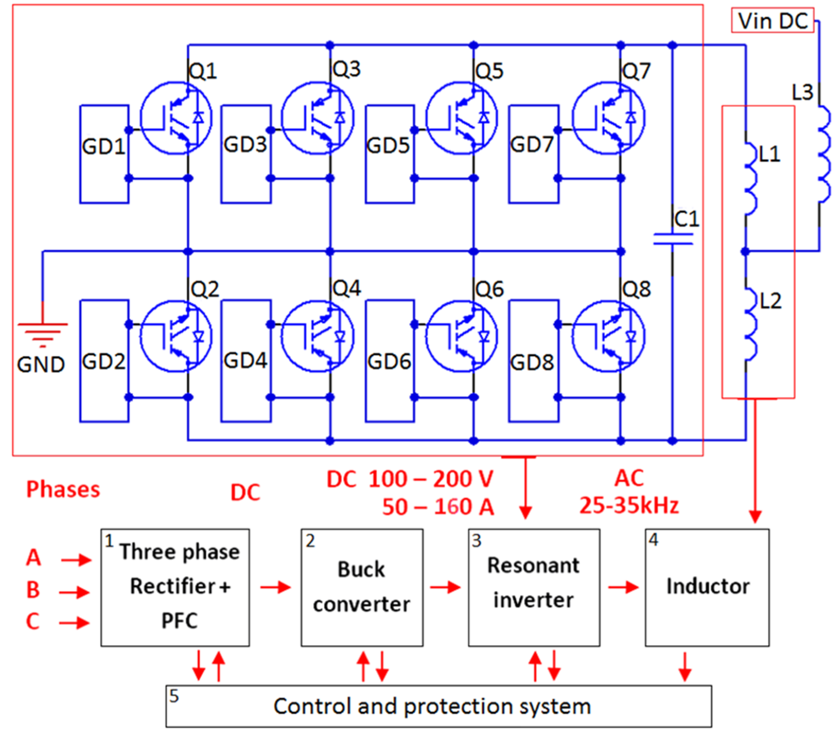
3. Experimental Setup

The experimental setup aimed to verify the designed inverter for induction heating based on paralleled IGBTs and the suggested methodology and to depict the current mismatch amongst the transistors experimentally. The experimental study was conducted as follows: converters were designed with 3, 4 and 5 transistors in parallel per side (Figure 1) following the presented step-by-step methodology in point 2; converters were manufactured using IGBTs listed in Table 1 Applications, using transistors from the same and different production lots; the derating factors and expected current mismatch were analysed according to the nominal current per inverter; the currents were measured through each transistor in parallel at full load during the entire melting cycle; the thermal differences were measured with an infrared camera on the heatsink surface. In addition, the layout and inductor construction improvements were implemented, leading to the minimisation of the oscillations.
Figure 6 shows an experimental model of the self-resonant converter for induction heating with its main components: 8 GIBT transistors, connected according to Figure 1; forced air cooling system with fans; resonant capacitor tank, inductor; and graphene crucible. The 4 selected transistors per side were considered according to previously presented Equations (1)–(16) with a current derating factor of 20%.
The experimental study was conducted at the maximum converter power to depict the current mismatch under worst-case conditions. The results are illustrated with oscillograms, as follows:
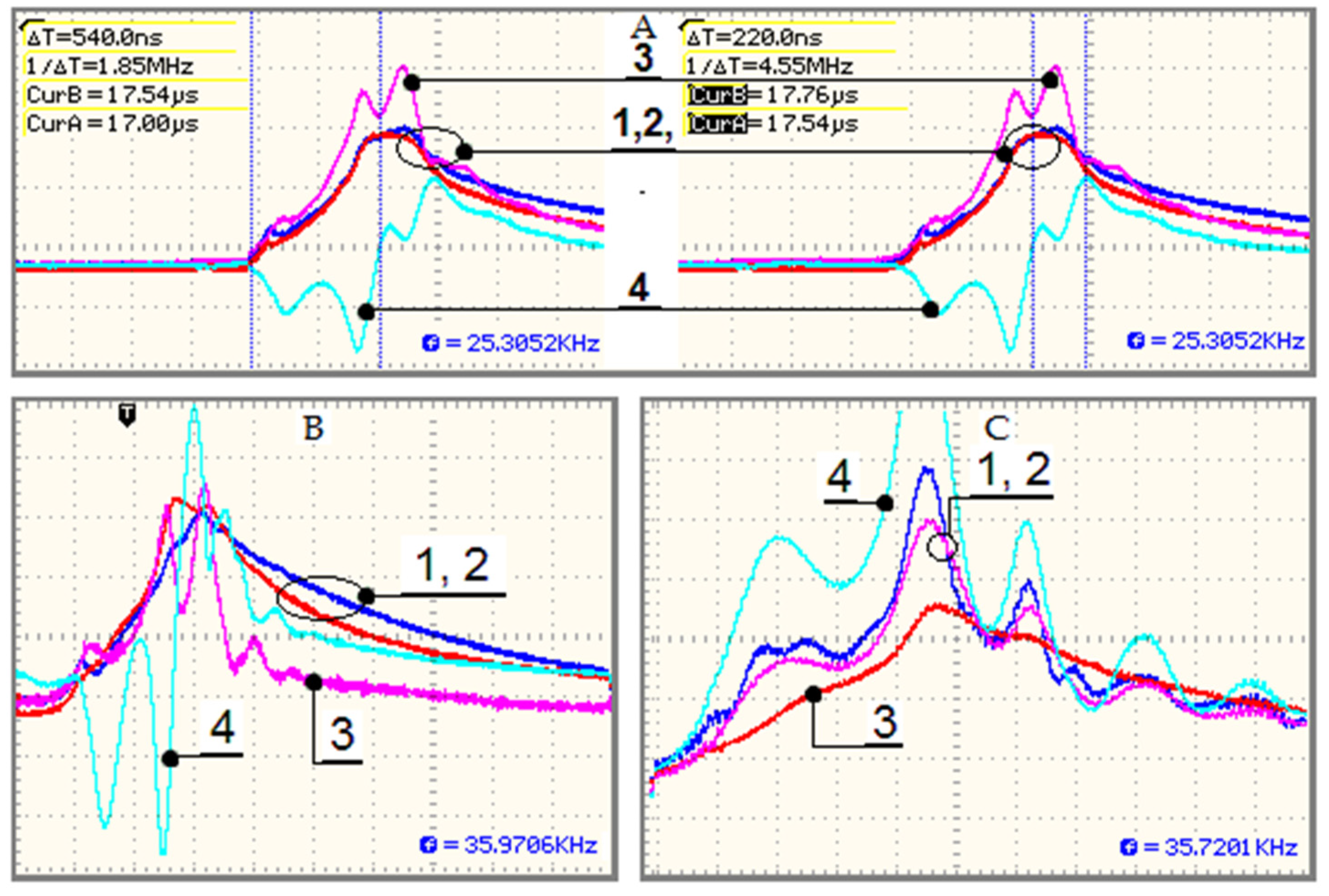
  • Figure 7. The oscillograms showed the expected current mismatch between transistors selected from the same production lot (1, 2) and transistors from two different lots (3, 4). Although all transistors were the same type, the first two conducted with a negligible difference, while transistor 3 showed a 25% higher current and transistor 4 switched on with a 540 ns delay (Figure 7A,B). The provided measurements clearly showed that a converter based on such a selection of IGBT transistors would be unreliable. In another selection, a different lot transistor (graphic 4, Figure 7C) could switch prematurely, conducting higher current, which is also an unacceptable condition.
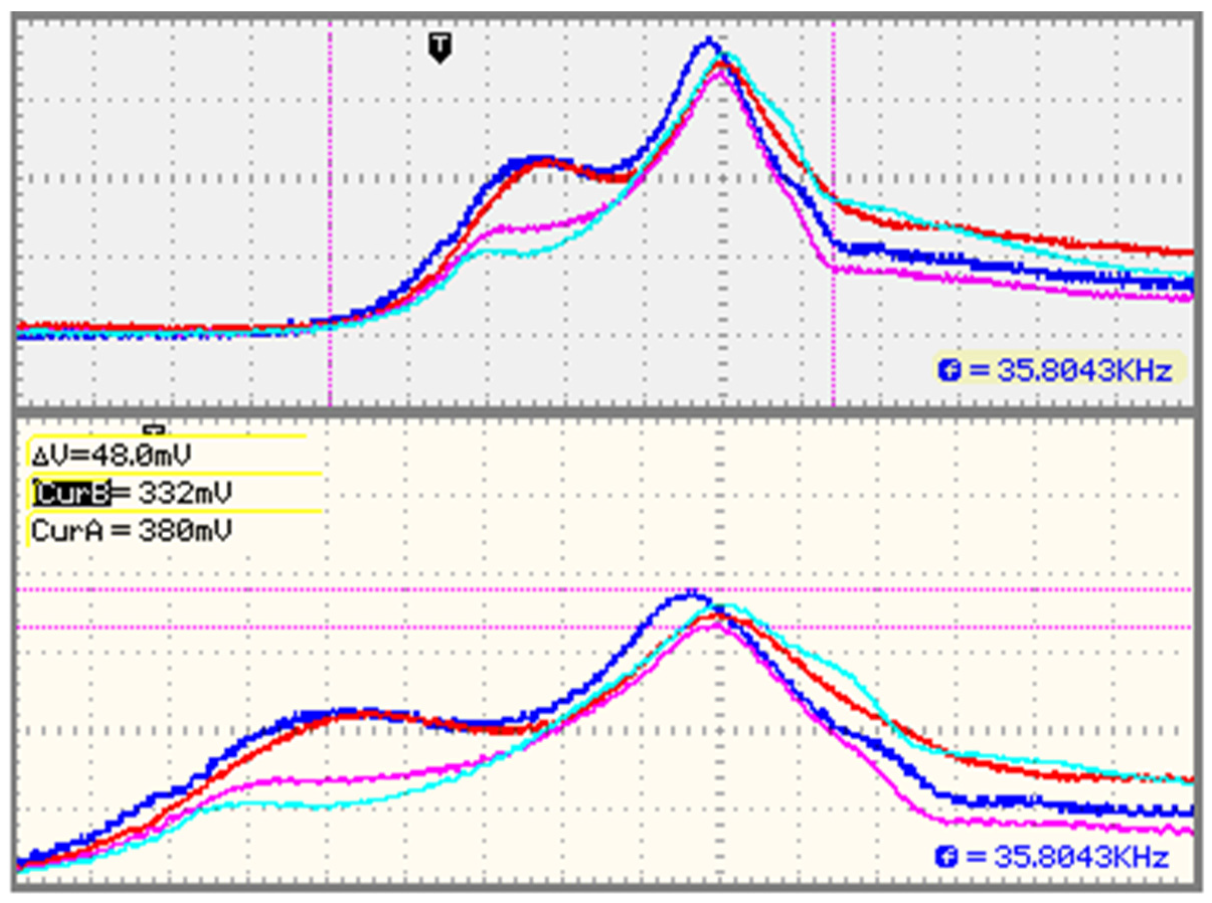
  • Figure 8. The oscillograms showed an acceptable current mismatch in the range of 2–5% at the peak point due to the layout issues and parasitic elements. The experiment was conducted in the following conditions: the transistors were selected from the same production lot; the resonant frequency during the entire heating process varied in the range 25–35 kHz, depending on the load conditions. The experimental result also confirmed the suggested current mismatch range of ±5% for the production lot. Similar results were received with the transistors shown in Table A1, Appendix A.
  • Figure 9. The oscillograms presented the operation of the converter, comprised of transistors in parallel. The experiment showed a stable process in the entire frequency and power range. According to Figure 9B, the sinusoidal voltage over the inductor crossed the zero point between both sides of the voltage precisely, which experimentally proved the inverter’s ability to operate in ZVS with correctly selected paralleled transistors.
  • Figure 10. The proposed inverter improved from the first unit (Figure 6) by moving the capacitor tank allocated in parallel to each transistor. Although the converter layout was not an object of this research, such a layout matched better the paralleled transistors as a current mismatch amongst the IGBTs under 2% was observed.
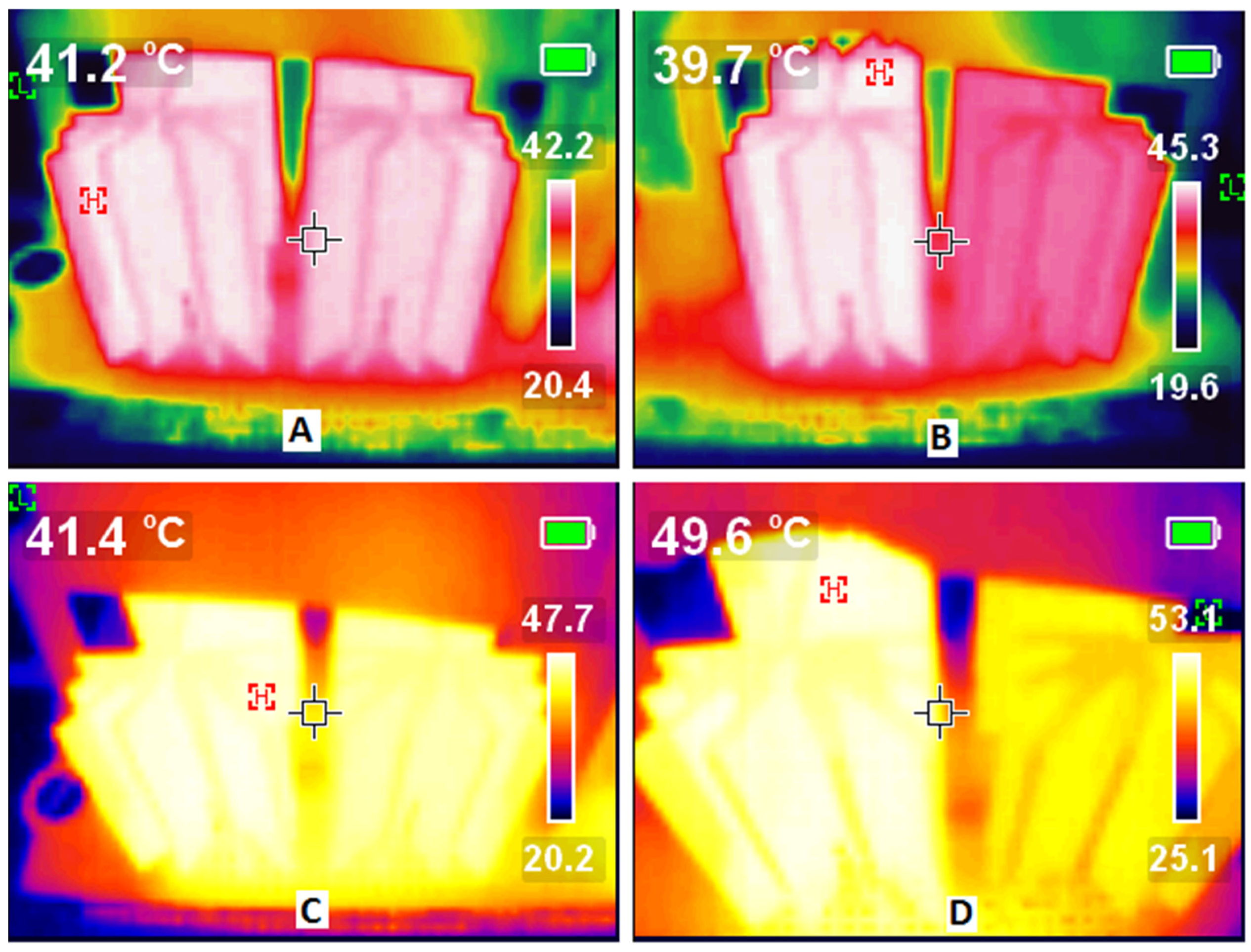
  • Figure 11. The presented thermal images provided an experimental measurement of the temperature on the heatsinks’ surface. Typically, the paralleled transistors have to be assembled on a typical heat sink, sharing and equalising the temperature. In this experiment, they were intestinally separated for the thermal difference to be better depicted. The investigation showed a thermal difference between transistors in parallel with low current differences (Figure 11A,C) according to Figure 8 and high current differences (Figure 11B,D) according to Figure 7B,C.
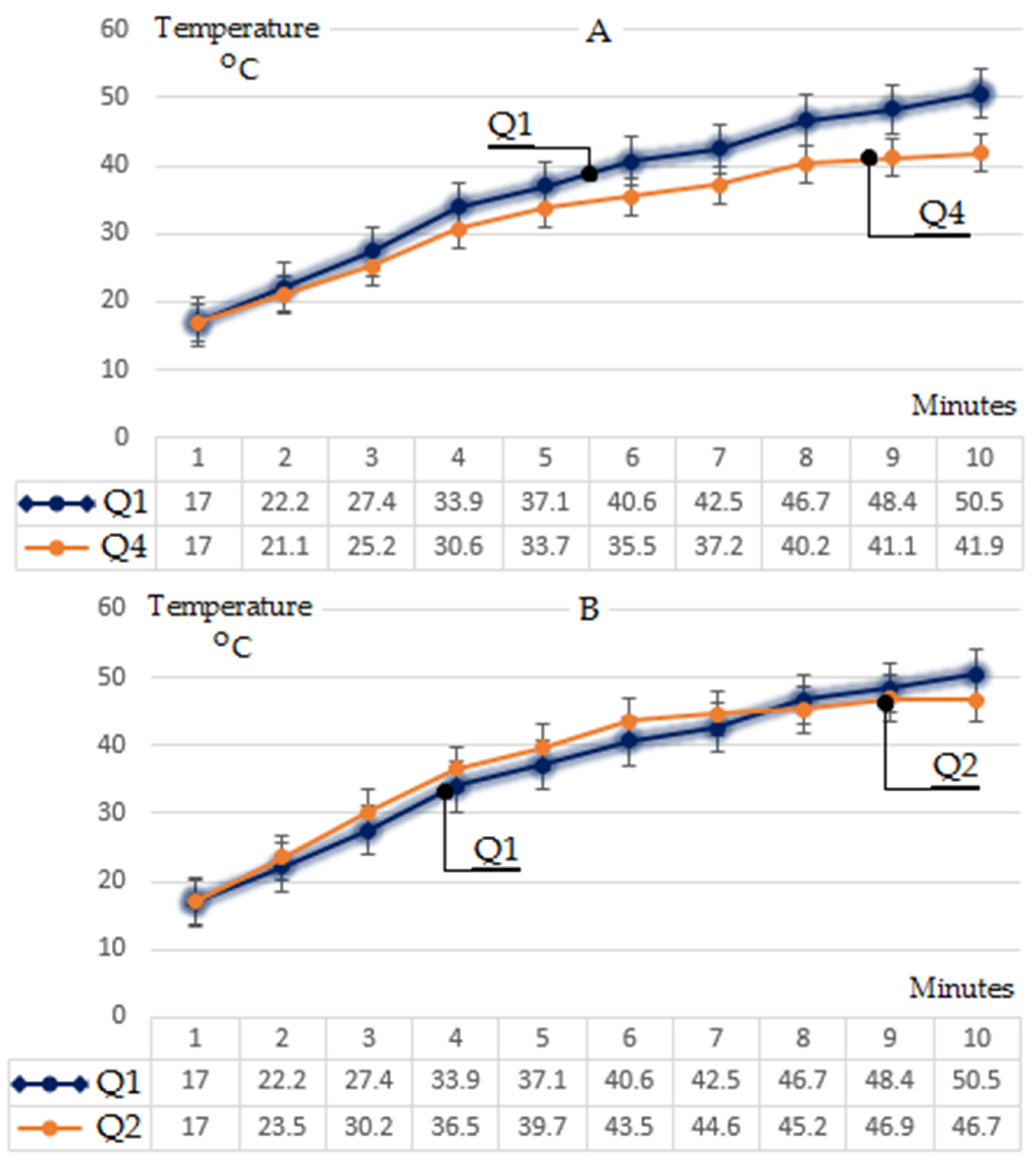
  • Figure 12. The thermal differences depicted as infrared pictures in Figure 11 are described as transient processes in an operation cycle. As Figure 12A shows, the thermal difference between transistors the Q1 and Q4 heatsink surface (Figure 7A) could reach 10 °C. The same experiment showed that the temperature difference under the worst-case conditions between transistors of the same production lot Q1 and Q2 (Figure 7A) could be minimised to 3–4 °C.
  • Figure 13. The crucible reached 500 °C for 10 min; enough for melting tin with a high energy efficiency. Potentially, the entire system can be designed for higher temperatures to melt other metals, requiring higher power and, hence, powerful transistors. The system was tested with several melting cycles, giving the established transistors and crucible temperatures without overheating.
  • Figure 14. The experiment showed oscillations that could potentially occur due to PCB layout issues in inverters with paralleled transistors. Usually, such oscillations occur in the gate drive circuit when transistors share the same gate drivers as the research in [51,52,53]. However, in this case, each transistor was controlled by an individual driver (Figure 1), and it was found that the problem originates from the conductors’ length and parasitics, which occur between the PCB and the inductor.
  • Figure 15 Although the above-described problems are beyond the scope of this research, a layout modification was suggested and used for all presented experimental tests. According to the circuit in Figure 15, the air-cooled inductor was divided into a number equal to the number of paralleled transistors sections. With this, the inductors L1, L3, L5 and L7 from the high side and L2, L4, L6 and L8 from the low side correspond to inductors L1 and L2 from Figure 1. Capacitors C1-C4, in summary, represent capacitor C1 from the resonant tangent in Figure 1. Although the effect of parasitics minimisation was experimentally observed, giving the inverter’s stable operation, this part requires future research and improvements.

4. Discussion

The provided experimental verification was performed with a resonant inverter for induction heating (Figure 6). As the main contribution in this research, the result showed that such a topology (Figure 1) can be completed with paralleled IGBTs, operating with low mismatch current and acceptable current difference amongst the transistors, which is supported by the presented oscillograms (Figure 7, Figure 8 and Figure 9). The achieved current sharing amongst the paralleled IGBTs makes the ZVS mode of operation possible for a resonant inverter with paralleled transistors, which is the main advantage of the investigated topology. The presented results showed the feasibility of the investigated topology for improving the installed power of the self-resonant inverters for induction heating. As it was experimentally shown that the installed capacity can reach more than 30 kW with four IGBTs in parallel per side of the topology, it can be concluded that such a modification is applicable for small laboratory or industrial induction crucible furnaces.
The suggested methodology for analysing the paralleled IGBT transistors is based on stipulated conditions in which the transistors’ static and dynamic parameters (Figure 3) are digitalised into polynomial Equations (3)–(8). The calculating procedure shows the expected parameters dispersion in a production lot (Figure 4). As a result, the necessary derating factor, the current mismatch, and the current difference amongst the paralleled transistors can be suggested (Figure 5). With this, the number of the necessary transistors in parallel can be calculated on the design level for the given application.
The temperature difference between the paralleled IGBTs, which results from the current mismatch, was in an acceptable range of several degrees Celsius. This final experiment verified the applicability of the suggested topology.

5. Conclusions

In this study, a methodology of the IGBTs’ parallel work estimation and its application in the design procedure of a self-resonant inverter for a crucible induction system was demonstrated. The presented step-by-step approach showed satisfactory results, giving the required derating factors and current mismatch between the transistors.
The investigated self-resonant converter based on paralleled transistors was applied to an induction crucible melting system. It was shown that the presented circuit has a stable operation mode in ZVS with paralleled transistors. The conducted experiments showed a satisfactory current share and temperature equalisation. It can be concluded that the circuit has the magnitude to reach an installed power of 50–80 kW with several powerful modules in parallel, giving budget-friendly induction melting systems with inverters with high power density.
The suggested methodology was based on stipulated data, i.e., Equations (3)–(6) were derived only for the concrete transistor, and it did not have diverse characteristics. Despite that, such an approach for analysis is highly applicable for practical design and experimental verification.

Author Contributions

Conceptualization, B.D.; methodology, B.D., K.H., S.B., G.C.; software, B.D.; validation, B.D.; formal analysis, B.D.; investigation, B.D.; resources, G.C.; data curation, B.D., K.H., S.B.; writing—original draft preparation, B.D.; writing—review and editing, K.H., S.B.; visualization, B.D.; supervision, G.C., K.H.; project administration, G.C.; funding acquisition, N/A. All authors have read and agreed to the published version of the manuscript.

Funding

This research received no external funding.

Institutional Review Board Statement

Not applicable.

Informed Consent Statement

Not applicable.

Data Availability Statement

Not applicable.

Conflicts of Interest

The authors declare no conflict of interest.

Appendix A

Table A1. IGBT transistors, suitable for experimental verification with resonant inverters for induction heating, operating with PTC.
IGBT TransistorPackage I C ( 25 ° C ) ( A ) V C E ( V ) P W ( 25 ° C ) ( W ) V G E ( t h ) /
V C E ( s a t ) ( V )
I C ( 25   ° C ) = 30–60 A
RGT60TS65DTO-247N556501947.0/2.1
DGTD120T25S1PTTO-2475012003487.0/2.4
FGA50N100BNTDTO-3P5010001567.0/1.8
RGW00TS65DTO-247N506502547.0/1.9
I C ( 25   ° C ) = 60–80 A
NGTB40N120FL2TO-264 3L7012003682.6/3.7
STGW39NC60VDTO-247706002505.75/2.4
IXA45IF1200HBTO-2477812003256.5/2.1
STGW40H65FBTO-3PF806502836.0/2.0
I C ( 25   ° C ) = 80–120 A
FGA60N60UFDTO-3P1206002986.5/2.4
FGA60N65SMDTO-3PN1206506006.0/2.5
NGTB50N120FL2TO-24710012005356.5/2.4
IRGP6690DPbFTO-247AD1406004836.5/1.95
Listing A1. Calculating the collector-emitter current (Ic) with polyval function in MATLAB:
clear
format short
Ic_max_hightemp = [0.0096; −0.106; −3.8721; 86.988; −600.32; 1365.2];
Vge = 9; % Vge = 9 V
polyval (Ic_max_hightemp, Vge)% ans = 56.99 A

References

  1. Davies, E.J. Conduction and Induction Heating; The Institution of Engineering and Technology IET: London, UK, 2007; ISBN 978-0-86341-174-8. [Google Scholar]
  2. Haimbaugh, R. Induction Heat Treating; ASM international: Materials Park, OH, USA, 2015; ISBN 978-1-62708-089-7. [Google Scholar]
  3. Lupi, S.; Forzan, M.; Aliferov, A. Induction and Direct Resistance Heating, Theory and Numerical Modeling; Springer International Publishing: Springer Cham Heidelberg, Germany, 2015; ISBN 978-3-319-03478-2. [Google Scholar]
  4. Rudnev, V.; Loveless, D.; Cook, R. Handbook of Induction Heating; Taylor & Francis Group: Boca Raton, FL, USA, 2017; ISBN 978-1-4665-5395-8. [Google Scholar]
  5. Rapoport, E.; Pleshivtseva, Y. Optimal Control of Induction Heating Processes; Taylor & Francis Group: Boca Raton, FL, USA, 2007; ISBN 978-0-8493-3754-3. [Google Scholar]
  6. Zinn, S.; Semiatin, S. Elements of Induction Heating. Design, Control and Applications; ASM International: Materials Park, OH, USA, 2007; ISBN 0-87170-308-4. [Google Scholar]
  7. Shokouhmand, H.; Ghaffari, S. Thermal Analysis of Moving Induction Heating of a Hollow Cylinder with Subsequent Spray Cooling: Effect of Velocity, Initial Position of Coil, And Geometry, Applied Mathematical Modelling 36; Elsevier: Amsterdam, The Netherlands, 2012; pp. 4304–4323. [Google Scholar]
  8. Li, F.; Ning, J.; Liang, S.Y. Analytical Modeling of the Temperature Using Uniform Moving Heat Source in Planar Induction Heating Process. Appl. Sci. 2019, 9, 1445. [Google Scholar] [CrossRef] [Green Version]
  9. Naar, R.; Bay, F. Numerical optimisation for induction heat treatment processes. Appl. Math. Model. 2013, 37, 2074–2085. [Google Scholar] [CrossRef]
  10. Zhou, X.; Thomas, B.; Hernandez, C.; Castillejos, A.; Acosta, F. Measuring Heat Transfer During Spray Cooling Using Con-trolled Induction-Heating Experiments and Computational Models, Applied Mathematical Modelling 37; Elsevier: Amsterdam, The Netherlands, 2013; pp. 3181–3192. [Google Scholar]
  11. Djambazov, G.; Bojarevics, V.; Pericleous, K.; Croft, N. Finite volume solutions for electromagnetic induction processing. Appl. Math. Model. 2015, 39, 4733–4745. [Google Scholar] [CrossRef] [Green Version]
  12. Jankowski, T.; Pawley, N.; Gonzales, L.; Ross, C.; Jurney, J. Approximate Analytical Solution for Induction Heating of Solid Cylinders. Applied Mathematical Modelling 40; Elsevier: Amsterdam, The Netherlands, 2016; pp. 2770–2782. [Google Scholar]
  13. Tavakoli, M.; Karbaschi, H.; Samavat, F. Influence of Workpiece Height on the Induction Heating Process. Math. Comput. Model. 2011, 45, 50–58. [Google Scholar] [CrossRef]
  14. Liu, Q.; Li, B.; Schlangen, E.; Sun, Y.; Wu, S. Research on the Mechanical, Thermal, Induction Heating and Healing Properties of Steel Slag/Steel Fibers Composite Asphalt Mixture. Appl. Sci. 2017, 7, 1088. [Google Scholar] [CrossRef] [Green Version]
  15. Dimitrov, B.; Streblau, M.; Marinov, A. An Approach for Designing a Complex Inductor—Workpiece System for Induction Heating Detail Systems. Technol. Educ. Manag. Inform. TEM J. 2014, 3, 244–249. [Google Scholar]
  16. Li, H.; Yu, J.; Wu, S.; Liu, Q.; Li, Y.; Wu, Y.; Xu, H. Investigation of the Effect of Induction Heating on Asphalt Binder Aging in Steel Fibers Modified Asphalt Concrete. Materials 2019, 12, 1067. [Google Scholar] [CrossRef] [Green Version]
  17. Vila-Cortavitarte, M.; Jato-Espino, D.; Castro-Fresno, D.; Calzada-Perez, M. Self-Healing Capacity of Asphalt Mixtures In-cluding By-Products Both as Aggregates and Heating Inductors. Materials 2018, 11, 800. [Google Scholar] [CrossRef] [PubMed] [Green Version]
  18. Fu, X.; Chen, Q.; Chen, X.; Zhang, L.; Yang, A.; Cui, Y.; Yuan, C.; Ge, H. A Rapid Thermal Nanoimprint Apparatus Through In-duction Heating of Nickel Mold. Micromachines 2019, 10, 334. [Google Scholar] [CrossRef] [Green Version]
  19. Aung, M.P.; Nakamura, M.; Hirohata, M. Characteristics of Residual Stresses Generated by Induction Heating on Steel Plates. Metals 2018, 8, 25. [Google Scholar] [CrossRef] [Green Version]
  20. Chamorro, X.; Herrero-Dorca, N.; Bernal, D.; Hurtado, I. Induction Skull Melting of Ti-6Al-4V: Process Control and Efficiency Optimisation. Metals 2019, 9, 539. [Google Scholar] [CrossRef] [Green Version]
  21. Namadmalan, A.; Moghani, J. Self-Oscillating Switching Technique for Current Source Parallel Resonant Induction Heating Systems. J. Power Electron. 2012, 12, 851–858. [Google Scholar] [CrossRef] [Green Version]
  22. Namadmalan, A.; Moghani, J.S.; Milimonfared, J. A Current-Fed Parallel Resonant Push-Pull Inverter with a New Cascaded Coil Flux Control for Induction Heating Applications. J. Power Electron. 2011, 11, 632–638. [Google Scholar] [CrossRef] [Green Version]
  23. Chamsuka, P.; Srinonchat, J. Study and development Inductance melting control system using low energy. Energy Procedia 2013, 34, 945–950. [Google Scholar] [CrossRef] [Green Version]
  24. Nagarajan, B.; Sathi, R. Phase Locked Loop based Pulse Density Modulation Scheme for the Power Control of Induction Heating Applications. J. Power Electron. 2015, 15, 65–77. [Google Scholar] [CrossRef] [Green Version]
  25. Qi, H.; Peng, Y.; Li, Y. The Study of Phase-shift Super-Frequency Induction Heating Power Supply. Phys. Procedia 2012, 24, 101–106. [Google Scholar] [CrossRef] [Green Version]
  26. Kawaguchi, Y.; Hiraki, E.; Tanaka, T.; Nakaoka, M. Basic Study of a Phase-Shifted Soft Switching High-Frequency Inverter with Boost PFC Converter for Induction Heating. J. Power Electron. 2008, 8, 192–199. [Google Scholar]
  27. Yachiangkam, S.; Sangswang, A.; Naetiladdanon, S.; Koompai, C.; Chudjuarjeen, S. Steady-State Analysis of ZVS and NON-ZVS Full-Bridge Inverters with Asymmetrical Control for Induction Heating Applications. J. Power Electron. 2015, 15, 544–554. [Google Scholar] [CrossRef] [Green Version]
  28. Qi, X.; Peng, Y.; Li, Y. Parameters Design of Series Resonant Inverter Circuit. Phys. Procedia 2012, 24, 133–138. [Google Scholar] [CrossRef] [Green Version]
  29. Wang, Y.; Li, Y.; Peng, Y.; Qi, X. Research and Design on IGBT Induction Heating Power Supply. Energy Procedia 2012, 16, 1957–1963. [Google Scholar] [CrossRef] [Green Version]
  30. Borage, M.; Tiwari, S. A 25 kW, 25 kHz Induction Heating Power Supply for MOVPE System Using L-LC Resonant Inverter, Hindawi Publishing Corporation. Adv. Power Electron. 2013. [Google Scholar] [CrossRef]
  31. Kumar, A.; Sadhu, P.; Mohanta, D.; Reddy, M. An Effective Switching Algorithm for Single Phase Matrix Converter in Induc-tion Heating Applications. Electronics 2018, 7, 149. [Google Scholar] [CrossRef] [Green Version]
  32. Han, W.; Chau, K.T.; Wong, H.C.; Jiang, C.; Lam, W.H. All-In-One Induction Heating Using Dual Magnetic Couplings. Energies 2019, 12, 1772. [Google Scholar] [CrossRef] [Green Version]
  33. Park, S.; Jang, E.; Joo, D.; Lee, B. Power Curve-Fitting Control Method with Temperature Compensation and Fast-Response for All-Metal Domestic Induction Heating Systems. Energies 2019, 12, 2915. [Google Scholar] [CrossRef] [Green Version]
  34. Lasobras, J.; Alonso, R.; Carretero, C.; Carretero, E.; Imaz, E. Infrared Sensor-Based Temperature Control for Domestic Induc-tion Cooktops. Sensors 2014, 14, 5278–5295. [Google Scholar] [CrossRef] [Green Version]
  35. Villa, J.; Artigas, J.; Barragan, L.; Navarro, D. An Amplifier-Less Acquisition Chain for Power Measurements in Series Reso-nant Inverters. Sensors 2019, 19, 4343. [Google Scholar] [CrossRef] [Green Version]
  36. Oh, Y.; Yeon, J.; Kang, J.; Galkin, I.; Oh, W.; Cho, K. Sensorless Control of Voltage Peaks in Class-E Single-Ended Resonant Inverter for Induction Heating Rice Cooker. Energies 2021, 14, 4545. [Google Scholar] [CrossRef]
  37. Tabaković, A.; Mohan, J.; Karač, A. Conductive Compartmented Capsules Encapsulating a Bitumen Rejuvenator. Processes 2021, 9, 1361. [Google Scholar] [CrossRef]
  38. Oncu, S.; Unal, K.; Tuncer, U. Laboratory setup for teaching resonant converters and induction heating. Eng. Sci. Technol. Int. J. 2021. [Google Scholar] [CrossRef]
  39. Areitioaurtena, M.; Segurajauregi, U.; Urresti, I.; Fisk, M.; Ukar, E. Predicting the induction hardened case in 42CrMo4 cylin-ders. Procedia 2020, 87, 545–550. [Google Scholar]
  40. Bortis, D.; Biela, J.; Kolar, J.W. Active Gate Control for Current Balancing of Parallel-Connected IGBT Modules in Solid-State Modulators. IEEE Trans. Plasma Sci. 2008, 36, 2632–2637. [Google Scholar] [CrossRef]
  41. Streit, L.; Janik, D.; Talla, J. Serial-Parallel IGBT Connection Method Based on Overvoltage Measurement. Elektron. Elektrotech. 2016, 22, 53–56. [Google Scholar] [CrossRef] [Green Version]
  42. Perez-Delgado, R.; Velasco-Quesada, G.; Roman-Lumbreras, M. Current Sharing Control Strategy for IGBTs Connected in Parallel. J. Power Electron. 2016, 16, 769–777. [Google Scholar] [CrossRef] [Green Version]
  43. Xue, Y.; Lu, J.; Wang, Z.; Tolbert, L.; Blalock, B.; Wang, F. Active Current Balancing for Parallel-Connected Silicon Carbide MOSFETs. IEEE Energy Conversion Congress and Exposition. 2013. Available online: https://0-ieeexplore-ieee-org.brum.beds.ac.uk/document/6646891 (accessed on 1 April 2021).
  44. Hu JAlatise, O.; Gonzalez, J.; Bonyadi, R.; Alexakis, P.; Ran, L.; Mawby, P. Robustness and Balancing of Parallel-Connected Power Devices: SiC Versus CoolMOS. IEEE Trans. Ind. Electron. 2016, 63, 2092–2102. [Google Scholar]
  45. Kimmer, T. Application Note, System Application Engineering IGBT, Reverse Conduction IGBT for Inductive Cooking, In-Fineon Technologies. 2012. Available online: https://www.infineon.com (accessed on 1 April 2021).
  46. Application Note, System Application IGBT, Reverse Conducting IGBT for Drives RC-Drives Cost-Optimized IGBT for Consumer Drive Application, Infineon Technologies 2010. Available online: https://www.infineon.com (accessed on 1 April 2021).
  47. Application Note AN4713, Induction Cooking: IGBTs in Resonant Converters, June 2015. Available online: www.st.com (accessed on 1 April 2021).
  48. Huang, X.; Chang, D.; Ling, C.; Zheng, T.Q. Research on Single-Phase PWM Converter with Reverse Conducting IGBT Based on Loss Threshold Desaturation Control. Energies 2017, 10, 1845. [Google Scholar] [CrossRef] [Green Version]
  49. Huang, X.; Ling, C.; Chang, D.; You, X.; Zheng, T.Q. Loss Characteristics of 6.5 kV RC-IGBT Applied to a Traction Converter. Energies 2017, 10, 891. [Google Scholar] [CrossRef] [Green Version]
  50. Application Note 5SYA 2098-00, Paralleling of IGBT modules, ABB Switzerland Ltd Semiconductors. Available online: https://library.e.abb.com/ (accessed on 1 April 2021).
  51. Application Note AN 17-001, IGBT Modules in Parallel Operation with Central and Individual Driver Board, Semikron. 2017. Available online: https://www.semikron.com/ (accessed on 1 April 2021).
  52. NXP UCODE G2XM SL3S1002AC2. 118. Available online: https://www.nxp.com/ (accessed on 1 April 2021).
  53. AND9100/D, Parallel of IGBTs, On Semiconductor. 2014. Available online: https://www.onsemi.com/ (accessed on 1 April 2021).
  54. Application Note AN 4544, IGBT Datasheet Tutorial. 2014. Available online: www.st.com (accessed on 1 April 2021).
  55. Roetzer, F.; Aschauer, A.; Jadachowski, L.; Steinboeck, A.; Kugi, A. Temperature Control for Induction Heating of Thin Strips. IFAC-PapersOnLine 2020, 53, 11968–11973. [Google Scholar] [CrossRef]
Figure 1. The electronic circuit of the proposed inverter for induction heating crucible melting furnace. Q1-Q8 IGBT transistors; GD1-GD8 gate drivers; C1, L1, L2 resonance tank; L3 induction heating inductor. A block diagram of the entire system for induction heating.
Electricity 02 00026 g001
Figure 2. Analysis of the number of IGBTs in parallel. (A) Number of transistors in parallel calculated in a derating range Δ = 0.1 0.5 , giving the necessary nominal current per transistor; (B) expected current through each transistor at the assumed maximum current of I m a x = 160   A ; (C) the targeted derating of Δ = 0.2 , i.e., 20%, is feasible with I C E n o m = 50   A , 4 IGBTs in parallel.
Electricity 02 00026 g002
Figure 3. (A) IGBT transconductance characteristic and its dependence on the temperature; NTC—Negative Thermal Coefficient; PTC—Positive Thermal Coefficient; ITP—Isothermal Point; (B) IGBT output characteristics and its dependence on the temperature.
Electricity 02 00026 g003
Figure 4. (A) Transconductance (dynamic) characteristics at nominal 25 °C (graphic 1 maximum and 2 minimum) and maximum 150 °C (graphic 3 maximum and 4 minimum) temperatures. (B) Output (static) characteristics at nominal 25 °C (graphic 1 maximum and 2 minimum) and maximum 150 °C (graphic 3 maximum and 4 minimum) temperatures.
Electricity 02 00026 g004
Figure 5. (A) Expected variation in the derating factor; (B) expected variation in the maximum current through the paralleled transistors. Graphics 1 and 2 at maximum and minimum thermal difference.
Electricity 02 00026 g005
Figure 6. A model of self-resonant converter for induction heating: 1—IGBT transistors; 2—resonant capacitor tank; 3—inductor; 4—graphene crucible. The used measurement equipment is as follows: oscilloscope RS PRO RSDS1204CFL; current probe ELDITEST CP6220; voltage differential probe Pico.
Electricity 02 00026 g006
Figure 7. Current mismatch amongst four paralleled IGBT transistors. (A,B) switched-on with a delay of transistor 4; (C) switched-on prematurely of transistor 4; 1, 2—transistors with the same production lot; 3, 4—two different production lots.
Electricity 02 00026 g007
Figure 8. Minimum current mismatch amongst four IGBT transistors from the same production lot.
Electricity 02 00026 g008
Figure 9. Operation of the inverter for induction heating. (A,B) 1, 2—voltages, respectively, over the paralleled high side (Q1, Q3, Q5, Q7—Figure 1) and low side (Q2, Q4, Q6, Q8—Figure 1) transistors; 3—current through the inductor; (B): 4—voltage crossing the zero switching point.
Electricity 02 00026 g009
Figure 10. Improving the converter construction, given in Figure 6.
Electricity 02 00026 g010
Figure 11. Infrared temperature measurements on the surface of the heatsink. (A,C) Appropriately selected transistors from the same production lot (Figure 7, graphics 1, 2); (B,D) transistors from different production lots (Figure 7 graphics 1, 4). The thermal measurements were performed with the infrared camera FLIR.
Electricity 02 00026 g011
Figure 12. Transistors thermal difference for one melting cycle of 10 min. (A) Between transistors Q1 and Q4; (B) between transistors Q1 and Q2, both selected according to Figure 7A.
Electricity 02 00026 g012
Figure 13. Infrared image of the graphene crucible, given in Figure 6.
Electricity 02 00026 g013
Figure 14. Oscillations due to PCB layout issues.
Electricity 02 00026 g014
Figure 15. A suggested structure of connection.
Electricity 02 00026 g015
Table 1. Digitalisation of the transconductance characteristics, shown in Figure 4A.
nominal characteristic
(Figure 2)
+5% data variation
Figure 3A, graphic 1
−5% data variation
Figure 3A, graphic 2
Nominal
temperature
25 °C
I C =
[ 0.0091 × V G E 5   0.1009 × V G E 4     3.6877 × V G E 3 82.845 × V G E 2     571.73 × V G E 1300.2           ]
I C =
[ 0.0096 × V G E 5   0.106 × V G E 4     3.8721 × V G E 3 86.988 × V G E 2     600.32 × V G E 1365.2   ]
I C =
[ 0.0087 × V G E 5   0.0959 × V G E 4 3.5033 × V G E 3 78.703 × V G E 2 543.15 × V G E 1235.2   ]
Nominal characteristic
(Figure 2)
+5% data variation
Figure 3A, graphic 3
−5% data variation
Figure 3A, graphic 4
Maximum
temperature
150 °C
I C =
[ 0.0278 × V G E 5   1.2169 × V G E 4 21.274 × V G E 3 186.96 × V G E 2 812.84 × V G E 1381.6           ]
I C =
[ 0.0292 × V G E 5   1.2777 × V G E 4 22.338 × V G E 3 196.31 × V G E 2 853.48 × V G E 1450.6         ]
I C =
[ 0.0264 × V G E 5   1.156 × V G E 4 20.211 × V G E 3 177.61 × V G E 2 772.2 × V G E 1312.5   ]
Table 2. Digitalisation of the output characteristics shown in Figure 4B.
nominal characteristic
(Figure 2)
+5% data variation
Figure 3B, graphic 1
−5% data variation
Figure 3B, graphic 2
Nominal
temperature
25 °C
I C =
[ 1.2487 × V C E 5   17.285 × V C E 4 96.404 × V C E 3 274.79 × V C E 2 342.33 × V C E 146.59   ]
I C =
[ 1.3112 × V C E 5   18.149 × V C E 4 101.22 × V C E 3 288.53 × V C E 2 359.45 × V C E 153.92   ]
I C =
[ 1.1863 × V C E 5   16.421 × V C E 4 91.583 × V C E 3 261.05 × V C E 2 325.21 × V C E 139.26 ]
Nominal characteristic
(Figure 2)
+5% data variation
Figure 3B, graphic 3
−5% data variation
Figure 3B, graphic 4
Maximum
temperature
150 °C
I C =
[ 0.0371 × V C E 5   0.7896 × V C E 4 7.2327 × V C E 3 34.392 × V C E 2 46.567 × V C E 18.897 ]
I C =
[ 0.039 × V C E 5   0.8291 × V C E 4 7.5943 × V C E 3 36.111 × V C E 2 48.895 × V C E 19.842 ]
I C =
[ 0.0353 × V C E 5   0.7501 × V C E 4 6.8711 × V C E 3 32.672 × V C E 2 44.238 × V C E 17.952   ]
Publisher’s Note: MDPI stays neutral with regard to jurisdictional claims in published maps and institutional affiliations.

