


Journal Menu
► ▼ Journal Menu-
- Nanomaterials Home
- Aims & Scope
- Editorial Board
- Reviewer Board
- Topical Advisory Panel
- Instructions for Authors
- Special Issues
- Topics
- Sections & Collections
- Article Processing Charge
- Indexing & Archiving
- Editor’s Choice Articles
- Most Cited & Viewed
- Journal Statistics
- Journal History
- Journal Awards
- Society Collaborations
- Conferences
- Editorial Office
Journal Browser
► ▼ Journal BrowserNeed Help?
Announcements
6 March 2024
Interview with Prof. Robert Hoye—Winner of the Nanomaterials 2023 Young Investigator Award
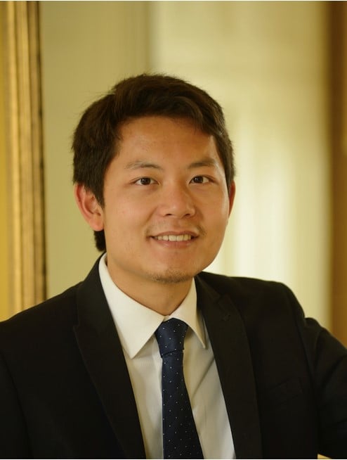
Name: Prof. Robert Hoye
Affiliation: Department of Chemistry, University of Oxford, UK
Research Interests: photovoltaics; nanocrystals; energy harvesting; photoelectrochemistry; X-ray detection; materials discovery; spatial atomic layer deposition
The following is an interview with Prof. Robert Hoye:
1. Could you briefly introduce yourself to our readers? What are you currently researching, and why did you choose this research field?
I am an associate professor of materials chemistry at the University of Oxford, UK, where I am also a fellow of St. John’s College. Previously, I was a research fellow at the University of Cambridge, UK (2016-2019) and lecturer at the Imperial College London, UK (2020-2022). I have had the privilege of supervising Ph.D. students at Cambridge, Imperial College, and Oxford, and have seen ten Ph.D. students graduate as well as two postdocs, who are now working in both academia and industry. My current group comprises of four postdoc and six Ph.D. students, and we are working on developing novel optoelectronic materials for energy conversion.
We have particularly contributed to the development of semiconductors with efficient charge–carrier transport through defect tolerance and band-like transport. We have used a combination of materials chemistry, spectroscopy, and computations, with the aim of unravelling the chemical–physical factors that enable these properties, in order to design more efficient solar absorbers. We have applied these materials in thin-film photovoltaics for energy harvesting for sustainably powered Internet of Things electronics, X-ray detectors, and photodetectors, as well as artificial-leaf devices that harvest sunlight to split water into fuels. In addition, we have developed a spatial atomic-layer deposition reactor that can precisely manufacture thin-film semiconductors onto nanostructured surfaces orders of magnitude faster than conventional atomic-layer deposition. I have recently contributed to creating a start-up company called NanoPrint Innovations Ltd. to commercialise this reactor, and I am the CTO of this company.
My group’s research is fundamentally interdisciplinary, and we utilize new insights to develop next-generation technologies that will have a positive impact on society, especially in the areas of energy and sustainability.
2. Which research topics do you think will be of particular interest to the research community in the coming years?
I think the inverse design of materials is a fascinating challenge. This is not just about AI or automation, but also about building on new insights that will guide the design of next-generation technologies. Defect tolerance is an especially exciting area, and could offer a new route to achieve efficient semiconductor devices, manufactured using cost-effective methods. The past decade of work on defect tolerance in metal-halide perovskites has opened up many questions, and unravelling the links between the many complex factors that influence how defects could be tolerated in materials is an important challenge for the field.
3. As a young researcher, what is the biggest challenge you have encountered in your research journey? How did you solve it?
The biggest challenge was securing my first academic position and building up a research group. I first became a PI through the Royal Academy of Engineering Research Fellowship, which I initially held at Cambridge. As a new PI, two of the biggest questions were: 1) how does one create a unique research platform that is recognised as distinct from those of previous supervisors, and 2) how does one compete for bright students in an environment with many other high-profile and well-established PIs? Fortunately, I was in a supportive environment and working across two “supergroups” – the Optoelectronics Group, and the Device Materials Group in Cambridge. These supergroups comprised of multiple PIs, and I was able to use the shared equipment to conduct independent research. At the same time, the highly collaborative and supportive environment provided a vibrant “ecosystem” for Ph.D. students to thrive in, and this helped spark the interest of talented students. After establishing a track record as an independent PI, it is always much easier to build up a research group. Getting started is always the hardest part.
4. Can you briefly describe the key to a happy laboratory life?
A highly collaborative and supportive research environment, where people are actively working together to solve problems together and discuss science in an open way.
5. If you have the opportunity, will you actively attend academic conferences? What do you think you can learn from participating in conferences that are different from working in a lab?
I regularly attend conferences across the world (Europe, UK, North America, Asia) in the areas of materials science, chemistry, photonics, and electronics. Meeting new people and discussing research is a very valuable way to start new collaborations and generate new ideas.
6. Which qualities do you think young researcheres need?
Patience, trust, strong communication skills, and a drive to keep on learning.
7. As the winner of this award, is there something you want to express, or someone to thank most
I would like to thank all of my mentors throughout my career, from my time as a student, to my time as a postdoc/research fellow, and also throughout my time as a PI.