Review

A Review on Lead-Free Hybrid Halide Perovskites as Light Absorbers for Photovoltaic Applications Based on Their Structural, Optical, and Morphological Properties

by
Shadrack J. Adjogri
1,2,* and
Edson L. Meyer
1
1
Fort Hare Institute of Technology, University of Fort Hare, Alice 5700, South Africa
2
Department of Chemistry, University of Fort Hare, Alice 5700, South Africa
*
Author to whom correspondence should be addressed.
Submission received: 9 September 2020 / Revised: 6 October 2020 / Accepted: 8 October 2020 / Published: 30 October 2020

Abstract

:
Despite the advancement made by the scientific community in the evolving photovoltaic technologies, including the achievement of a 29.1% power conversion efficiency of perovskite solar cells over the past two decades, there are still numerous challenges facing the advancement of lead-based halide perovskite absorbers for perovskite photovoltaic applications. Among the numerous challenges, the major concern is centered around the toxicity of the emerging lead-based halide perovskite absorbers, thereby leading to drawbacks for their pragmatic application and commercialization. Hence, the replacement of lead in the perovskite material with non-hazardous metal has become the central focus for the actualization of hybrid perovskite technology. This review focuses on lead-free hybrid halide perovskites as light absorbers with emphasis on how their chemical compositions influence optical properties, morphological properties, and to a certain extent, the stability of these perovskite materials.

1. Introduction

The evolving photovoltaic technologies have recently made possible the change of sunlight into electrical energy with elevated power conversion efficiencies at little expense [1]. Electrical energy is a highly suitable and harmless energy for daily human utilization. The industrial and consumer need for electrical energy is quickly growing. Hence, the need for continuous production of electrical energy from the sun’s energy is of paramount importance since it is unpolluted, renewable, plentiful, and natural [2]. Amongst the emerging photovoltaic technologies, perovskite solar cells have speedily ascended to the frontline as possible devices for electricity production [3,4]. Perovskite solar cells hold recorded high conversion efficiency of 29.1% in the photovoltaic research field [5]and are of low cost [6,7,8,9].
Perovskite compounds are made from different inorganic and organic material compositions [10]. Hybrid perovskite materials occur primarily as metal halide coordinated semiconductors by the common formulation of (RNH3) MX3 (R = CnH2n+1; X = halogen I, Br, Cl; M = Pb, Sn, Ge, etc.) with exploratory attributes of forming varied chemical composition and structures. They have the intrinsic tendencies of forming cubic composition (space group Pm3m), thereby being characterized through the regularly assembling solid ABX3, in which B represents the metal positively charged ion, and X denotes a halogen negatively charged ion [11]. During the past century, the creative family of these compounds has been duly researched, and it was discovered that they possess unique physical properties that are of great benefit to material science. The noteworthy physical properties are colossal magnetoresistance, ferroelectricity, and superconductivity [12]. By extension of their versatility, the materials are known to have unique photophysical properties which include tunable bandgap, a high absorption coefficient, long charge carrier (electron–hole) diffusion length, and low-temperature solution processability [13]. At different operating conditions, the perovskite materials are formed through synthesis, purification, and identification processes whereby at very high temperatures in the range of greater than 1300 K, they are routinely synthesized by solid-state mixing of constituent elements or compounds. Moreover, they have been synthesized through other methods such as by dehydrating the solution of precursor salts wherein the ones presenting expressions of semiconductor characteristics display significant application in the area of printable electronics due to their solution processability [14]. In the field of photovoltaics, the chemical composition of perovskite compounds is known to control the photovoltaic and optical properties of perovskite solar cells [15,16].
By stringent rules and standards, perovskite materials are being designed by using measurable confirmation tools to form unique chemical compositions using desired component properties. The measurable spatial arrangements of ABX3 perovskite compounds are conceivably being designed using the Goldschmidt tolerance (t) and the octahedral factors (μ). The Goldschmidt tolerance can be expressed by t = (RA + RB)/√2(RB + RX), in which RA, RB, and RX stand for the ionic radii of A, B, and X ions, respectively [15,17,18,19,20,21,22,23,24]. The octahedral factor is shown as μ = RB/RX [15,18]. The chemical interactions between constituent elements and ions are not accounted for by empirical schemes of the tolerance and octahedral factors. The structure of halide crystals would be empirically designed when t ranges from 0.813 to 1,107 and μ from 0.442 to 0.895.38. The assumption that the ionic radius is constant regardless of temperature and that ions are rigid spheres, including organic ions, is used for the calculation of the tolerance and octahedral factors [15]. Therefore, it is well known that a metal halide perovskite can be formed based on three peculiar factors: (1) the materials must be made up of anions and cations, in which there must exist a charge neutrality between the negatively charged ions and positively charged ions; (2) the materials’ octahedral factor must be calculated whereby the octahedral factor μ tends to envisage the stability of the BX6 octahedron; and (3) the material formation strategy must meet the basic features of the Goldschmidt tolerance factor t for the ionic radii of A, B and X [25].
Due to their outstanding electron–photon conversion efficiency, simplicity of assembly, and remarkable tolerance defects, a significant interest in the study of metal halogen-centered perovskite compounds has been witnessed in the past decades. In particular, the Pb-based halide perovskites in solar cells have shown high performance due to high absorption and emission efficiencies in connection with direct bandgaps [26]. Nevertheless, the significant limitations of Pb-based halide perovskites for their practical usage and marketability are due to the harmfulness of lead compounds and the low photostability of lead-based halide perovskites [27]. Over the years, intensive research has been carried out in a bid to mitigate the problem of lead in the industry. Based on the purpose of overcoming the limitations, theoretical studies have shown that the perovskite composition and the dormant Pb 6s subshells are partially accountable for the excellent photovoltaic characteristics of the Pb-based halide perovskites. Research has shown that other cations comprise dormant outward subshell s energy levels and that they are environmentally benign. These cations, Ge2+, Sn2+, Sb3+, Bi3+, and Cu2+, substitute Pb2+ to form Pb-free perovskites. As such, the growing exigency in the non-hazardous constituents of light-harvesting compounds has recently led towards the advancement of Pb-free perovskite solar cell devices [28].
The progress in perovskite coordination can be understood in two ways: morphological optimization and compositional coordination. The morphological optimization was enabled by the basic conception of the photo-electrical characteristics of perovskite. From previous research findings, it has been depicted that perovskite morphology has been changed from dots to bulk in the very recent state-of-the-art technology. In terms of compositional coordination, single cation-based and single halide-based perovskites have changed into structures with multiple cations and anions to provide superior properties and stability [29]. Furthermore, through tailoring of the chemical configuration, nanostructuring, and quantum confinement, bandgap engineering in the class of materials is achieved accordingly [30]. This research, therefore, shall focus on using chelating nitrogen materials for morphological optimization and compositional engineering to provide superior photo-electrical properties and stability.
This review article mainly discusses the replacement of lead via both homo and heterovalent replacement and their impact on the halide perovskite materials and photovoltaic properties. Furthermore, the collective outcomes from the investigational studies on the lead-free metal perovskite are discussed with emphasis on how chemical composition influences optical and morphological properties, and limitations for future studies are identified.

1.1. Pb Content of Perovskite and Crystalline Silicon Solar Cells

Presently, the most commonly operated and the more stable perovskite solar cell (PSC) devices utilize Pb salts as light-harvesting materials, but these lead salts contaminate the environment with an intense impact on human health. In the scientific community, the argument concerning the environmental effect of halide perovskites is still generating concerns and currently remains under debate because systematic investigations are not available [31]. Scientists have pointed out that one of the possible ways to resolve the problem of toxicity is through the reduction of the quantity of Pb salt in halide perovskite. Nevertheless, the question of how much Pb is accommodated in perovskite solar cells remains. Another vital question is: can this quantity be compared with lead-incorporating devices such as batteries? Life cycle assessment has been improvised as a functional unit to analyze environmental impacts caused by solar cell devices via the comparison of different devices and applications. For instance, a risk assessment using the “functional unit” has been used to analyze the Pb content in benchmark CH3NH3PbI3-based perovskite solar cells. An evident meaning of the “functional unit” is whereby calculations are performed on the quantity of electric current generated (1 kWh) by way of solar cells as well as through the disturbance that is required to undertake a lifetime on behalf of the solar cells [32].
Li and co-workers recently came up with an estimation procedure to determine the Pb content in PSCs, whereby they used three different perovskite compositions to exhibit the evaluation of Pb content. A calculation was carried out in order evaluate the lead content in the MAPbI3 perovskite composition by using parameters such as molar mass (620 gmol−1), the mass percentage of Pb (207/620 = 33.39%), and density (4.09 gcm−3) to give the required mass of Pb per unit area, which stands at around 0.75 gm−2 in support of a typical 550 nm-thick film. Likewise, FAPbI3 has a calculated mass of about 0.74 g m−2 of Pb per unit area when using a 32.7% Pb mass percentage and 4.10 g cm−1 density. From the weighted average of a mixture of MAPbBr3 (3.83 gcm−3), FAPbI3 (4.10 gcm−3), and CsPbI3 (5.39 gcm−3), a hybrid perovskite structure of (CsPbI3)0.05(FAPbI3)0.85(MAPbBr3)0.15 was estimated to have a 33.7% mass percentage of Pb and a 4.12 gcm−3 density, thereby resulting in the mass of Pb per unit area being around 0.76 gm−2 [33].
Meanwhile, the Pb content is measured in relation to its unit area concentration of Pb valued at around 0.75 gm−2 based on a standard 550 nm-thick lead (Pb)-based PSC, and it is known to be one hundred times greater in magnitude compared to that of current-day Pb content in paints valued at around 0.007 gm−2. Nevertheless, it is a degree of magnitude smaller than that for Pb-based paints (around 10 gm−2) which resulted in it being outlawed. When the perovskite devices are subjected to mild environmental damage, improved material insulation can decrease Pb outflow from such appliances. However, the development of desirable strategies can reduce or avoid the possible Pb outflow on the way to the surroundings in the case of air, groundwater, or soil. It is well known that designs aimed at glass insulation to tackle combustion hazards have been recorded, but the water opening to the water-susceptible perovskite film and the successive unalterable leakage of Pb in the direction of flow to groundwater and/or soils are focused on [33].
For the manufacture of Si solar cells, metallization exists as a key process step [34]. To date, the fabrication of nearly all the commercial Si solar cells has been achieved through the metallization of screen-printed silver (Ag) paste and at a minimum 20% boost in efficiency through the refining process of Ag paste metallization. Ag paste is prepared with three constituents: Ag powder, glass frit, and an organic carrier, whereby in the course of preparation, the glass frit has its content tuned from 0% to 2.5 weight%, and the Ag powder as well as the organic carrier are mixed at 87.5–90 weight% and 7.5–10 weight%, respectively. The organic carrier is a combination of a solvent (e.g., terpilenol), thickener (e.g., ethocel), plasticizer (e.g., phthalate), surfactant (e.g., caprylic acid), thixotropic agent (e.g., hydrogenated castor oil), and other additives [35]. The glass frit is a Pb-based compound and is a fundamental constituent in conductive silver dense film pastes that carry out an essential function in the metallization development of the pastes that have been employed widely in fusion circuits, solar energy cells, microelectronic packages, and other appliances based on outstanding electrical performance [36].
The average deduction of life cycle assessment studies, notwithstanding these deviations in lead impact effects, states that lead-based PSCs do not cause more inconveniences that obstruct substantial production and distribution when related to other marketable photovoltaic know-hows, such as crystalline silicon solar cells in the valuation of an incomplete product life cycle from resource extraction to the factory [32].

1.2. Composition Engineering

Composition engineering has proven to be an active approach to tailor the characteristics of perovskites and enhance the functioning of PSCs. The merits of perovskites with different cations are combined due to the mixing of the monovalent cations, which is one of the greatest commonly employed techniques in composition engineering of most perovskite materials [37]. Through the use of different incorporation of various elements, perovskites can form multi-layered compositions on the same chemical formula, which makes them versatile and highly attractive [38]. Therefore, the designs of organic–inorganic halides for specific applications, including materials for lighting and scintillators, can be achieved through the control of structural dimensionality and chemical compositions. Using the formation of mixed halide, A–B–X (A = organic positively charged ions, B = metallic positively charged ions, X = halide negatively charged ions) for the consideration of compositional and structural tunability, a variety of substitutions based on this principle could be effected out by focusing on each of the A, B and X positions. The control of the compound’s dimensionality can be achieved through the modification of organic cation magnitude through A-site replacement, thereby allowing thee materials to be liberally changed from 0 cluster combinations to 3D systems. By adding to the magnitude effects to compositional engineering of hybrid halide ABX3, the substitution of B and X sites permits fine-tuning of electronic configuration and optoelectronic characteristics since the B and X component states are the leading donors to the state regarding the Fermi level [39].
The perovskite arrangement of both the crystal composition and ion governs its structural, optical, and electronic properties, thereby establishing their structure–property relationship [38]. For instance, the various compositions of the perovskite-performing layer will change their respective trait and photophysical effects of the compound films. Moreover, the concentration of reactants in the solution has a superior influence on the morphology of the perovskite film, which eventually impacts the conversion efficiency of the solar cells [40].

1.3. Bandgap Engineering

Solar energy is intensely directed in the visible and near-infra-red (NIR) regime. Therefore, the choice of perovskite materials as a solar absorber for light-harvesting relies on the broad and intense absorption above the visible to the near infra-red domain of the solar spectrum [10,41]. The bandgap is the basic characteristic of a light harvester which controls the maximum theoretical power conversion efficiency. It is recognized to possess direct control by way of the actual performance of the perovskite cell device. It is also a property that determines whether the perovskite compound can either absorb the light particle within the visible spectrum or decline the absorption [42]. Since the bandgap is directly accountable for determining the potency (voltage) of the solar cell electric field, coupled with a situation in which the bandgap is too small, the device is able to collect extra current at the expense of possessing a small open-circuit voltage (VOC). However, in a situation in which the bandgap is too wide, such as 2 eV, it is a minor portion of the solar energy that can be absorbed. Therefore, an ideal bandgap tailored for a semiconductor stands at about 1.4–1.6 eV, and the same optical value is fined tuned for solar cells which are usually exhibited by distinct compounds [10,41].
The tunability of a direct bandgap is directly controlled by the composition choices of metal, halogens, and organic cations. Meanwhile, the compositional choices of metal, halogens, and organic cations can also lead to a variety of perovskites with different properties [43]. There are two major strategies for bandgap tuning: (i) Through chemical modification that entails changing the halogens (I−, Br−, Cl−). Through the atomic number progression of halogens, the electronegativity is reduced, thereby becoming similar to the values of the transitions metals with s2 electronic configuration, excluding lead (II) due to toxicity. (ii) Through chemical modification that entails the changing of the organic cation which is known for tuning the bandgap. Depending on their size, the organic cation controls the degree of metal halide orbital overlap, thereby causing the A-site to alter the valance and conduction band energies as well as the bandgap [44]. Due to the changing of organic cations, the other properties of the hybrid perovskite are manipulated, such as stability, charge separation abilities, carrier transport, etc. [45]. All of the perovskite lattice sites can undergo chemical substitution, therefore, it is essential to identify the chemical peculiarity amidst the three methods. For instance, the 3D perovskite with a common formula of ABX3 shows the importance of rich chemical replacement. A-site substitution of the perovskite material does not precisely provide the frontline electronic configuration, but it can exhibit an implied control by varying the crystal composition. Meanwhile, replacement at the B-site plays a major role in altering the conduction band, which, in turn, alters the electronic characteristics of the material. For X-site substitution, the anions dictate the valence band energy. Upon halide substitution of the perovskite material, the observed bandgap changes due to the influence through the energy levels of the negatively charged ions that are moving by way of the Cl–Br–I hierarchical pattern, whereby the energy bandgap changes due to the variation in the valence band structure that is moving by way of the 3p–4p–5p hierarchical orbital pattern with a monotonic reduction in the minimum amount of energy required to remove the electrons from the chemical atoms as the negatively charged electrons [46].

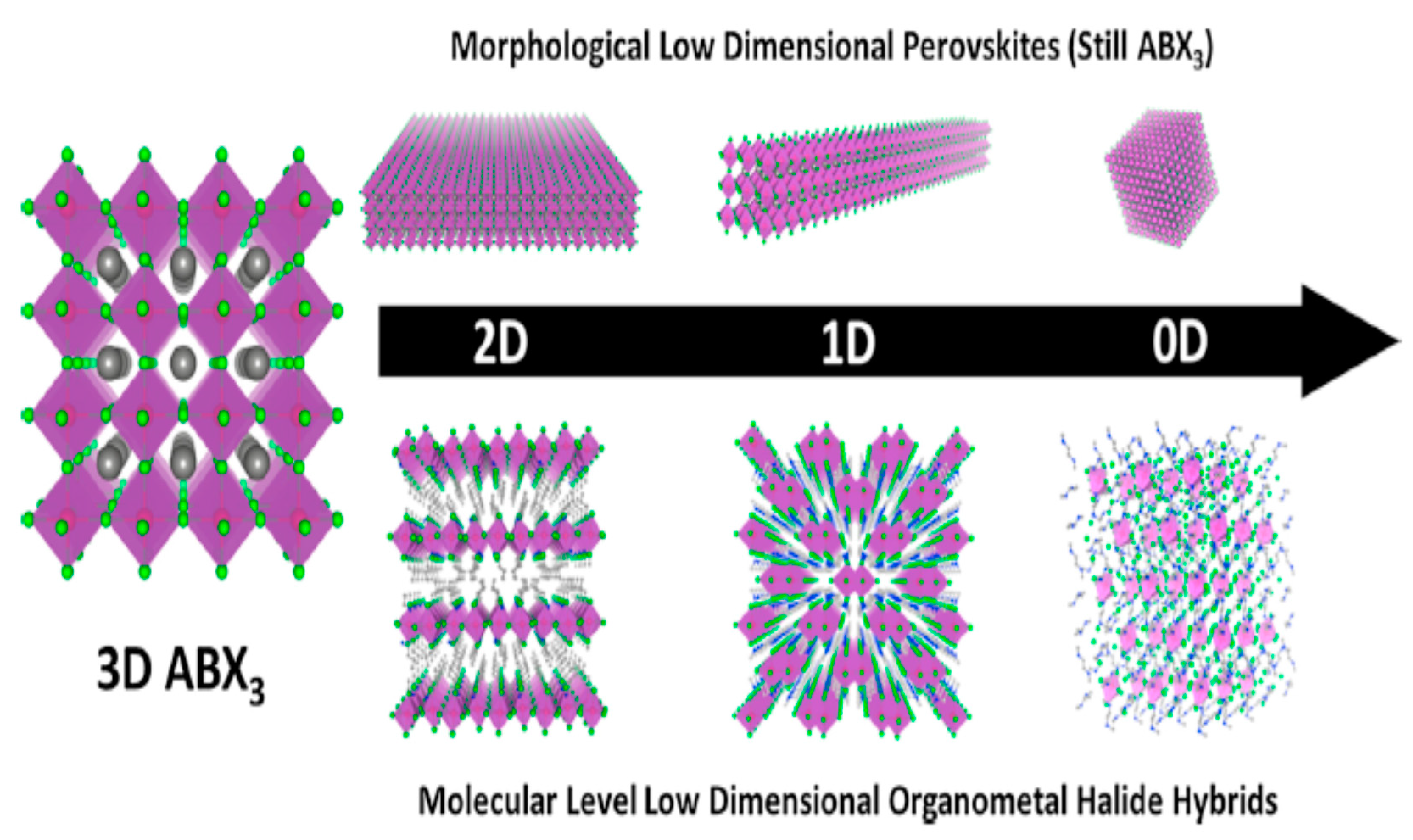
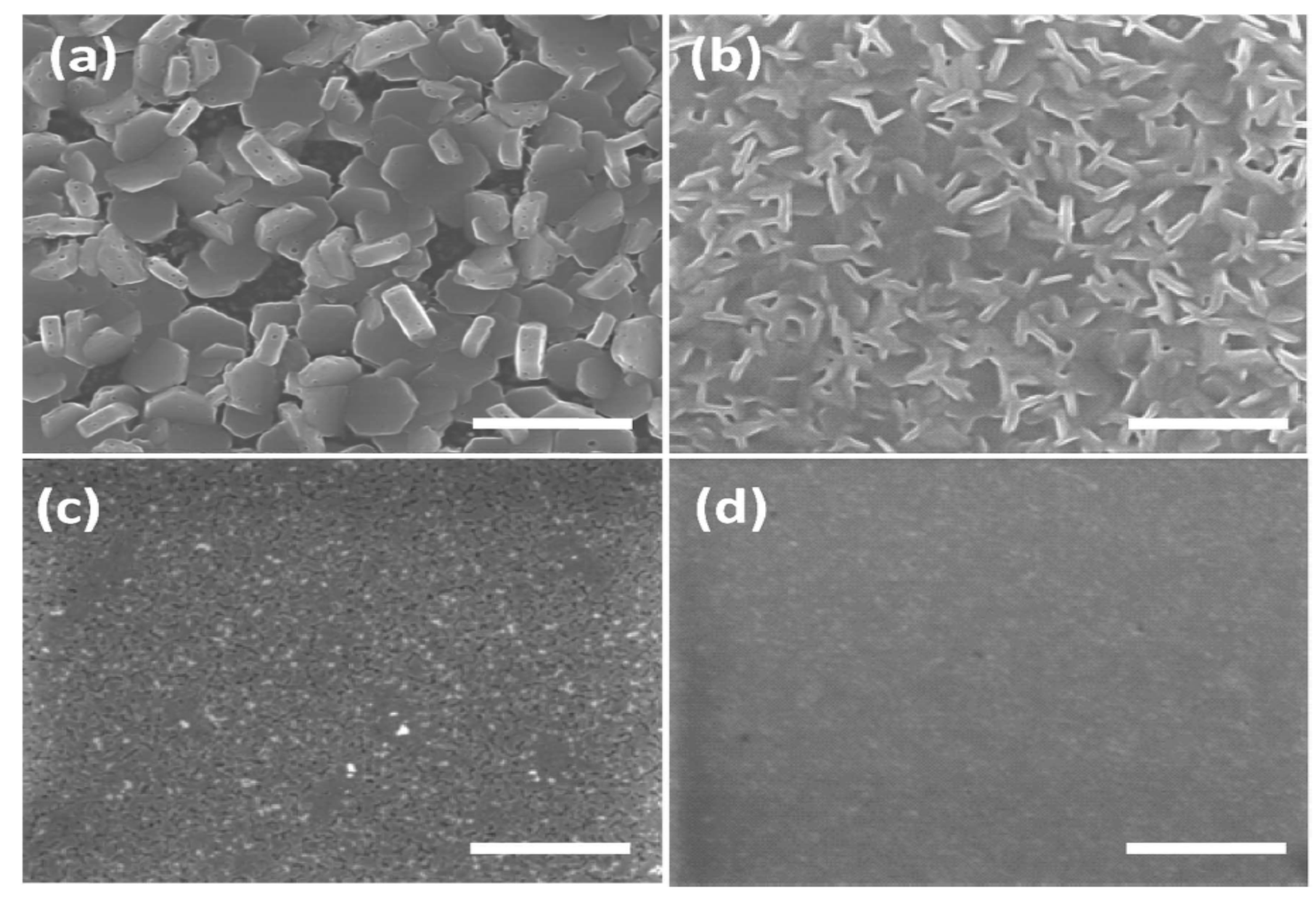
1.4. Morphology Engineering

Morphology, according to IUPAC, signifies shape, optical appearance, or form of phase domains in materials. From nanoscale to the macroscale, morphology is well known to perform a fundamental responsibility in the performance and properties in regard to the field of halide perovskites [47]. Therefore, the overall photovoltaic device performance significantly centers on the morphology, stoichiometry, and crystallinity of the materials [48]. In other words, perovskite layers must have distinct granule configuration, broad surface coverage, and small surface roughness to allow for recognition of an efficient solar cell [49]. As such, the deposition method of the perovskite material is of paramount importance, as confirmed by the experimental works of Burschka et al. and Bi et al. showcasing all the treatments and conditions that the materials undergo as part of and/or following the conversion to the final perovskite form. For instance, a recent report on power conversion efficiencies (PCEs) of over 15% from a planar model heterojunction perovskite solar cell was attributed to the development of extremely homogeneous flat films of the hybrid halide perovskite by vapor deposition [48].
The preparation of the perovskite thin films can be performed by various procedures such as vacuum evaporation deposition, solution-based methods, and the low-temperature vapor-assisted solution process. The dual-stage solution route deposition procedure was demonstrated to be the best amidst the various techniques, particularly due to its usefulness for preparing films of organic−inorganic complexes, in which the organic part is hard to evaporate, and/or for complexes in which the inorganic and organic parts have unsuitable solubility properties [49]. Furthermore, Sanders et al. reported that to optimize the morphology of perovskite compounds, the control of the perovskite precursors’ concentration in solution and that of the rotation speed should be particularly implemented [50].

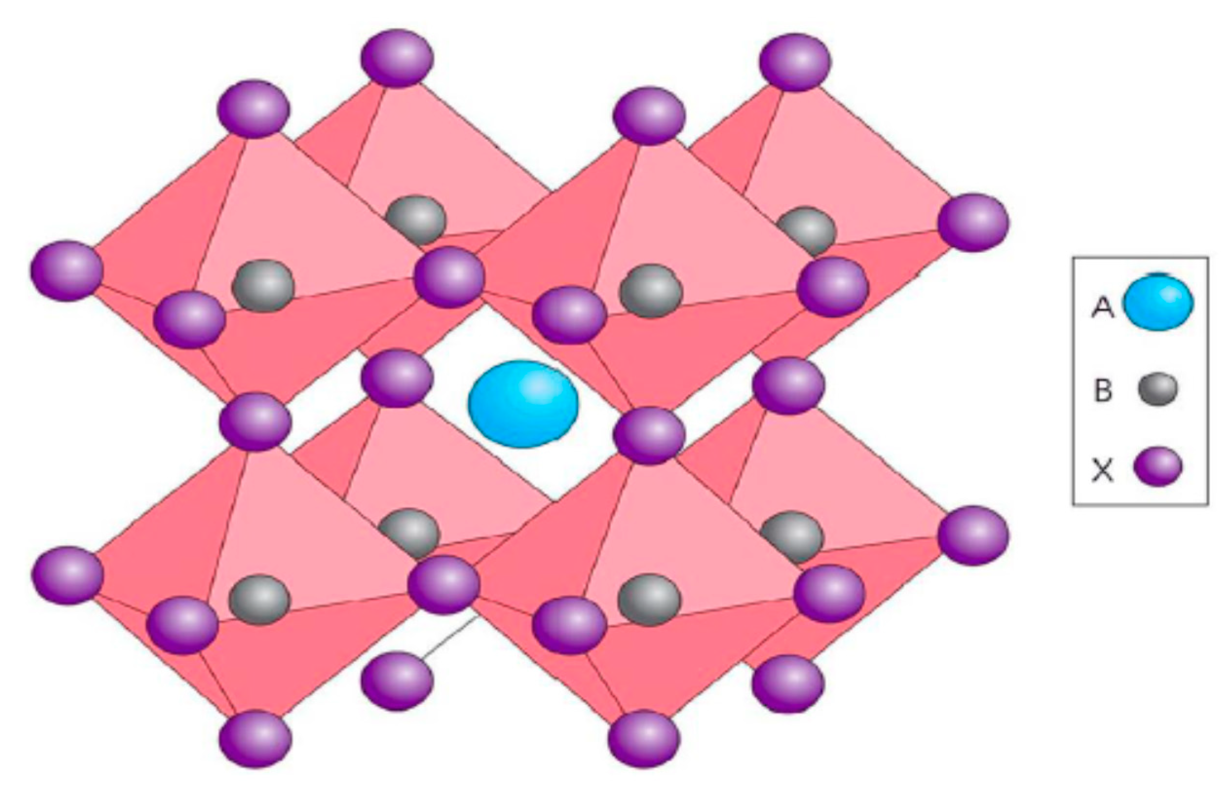
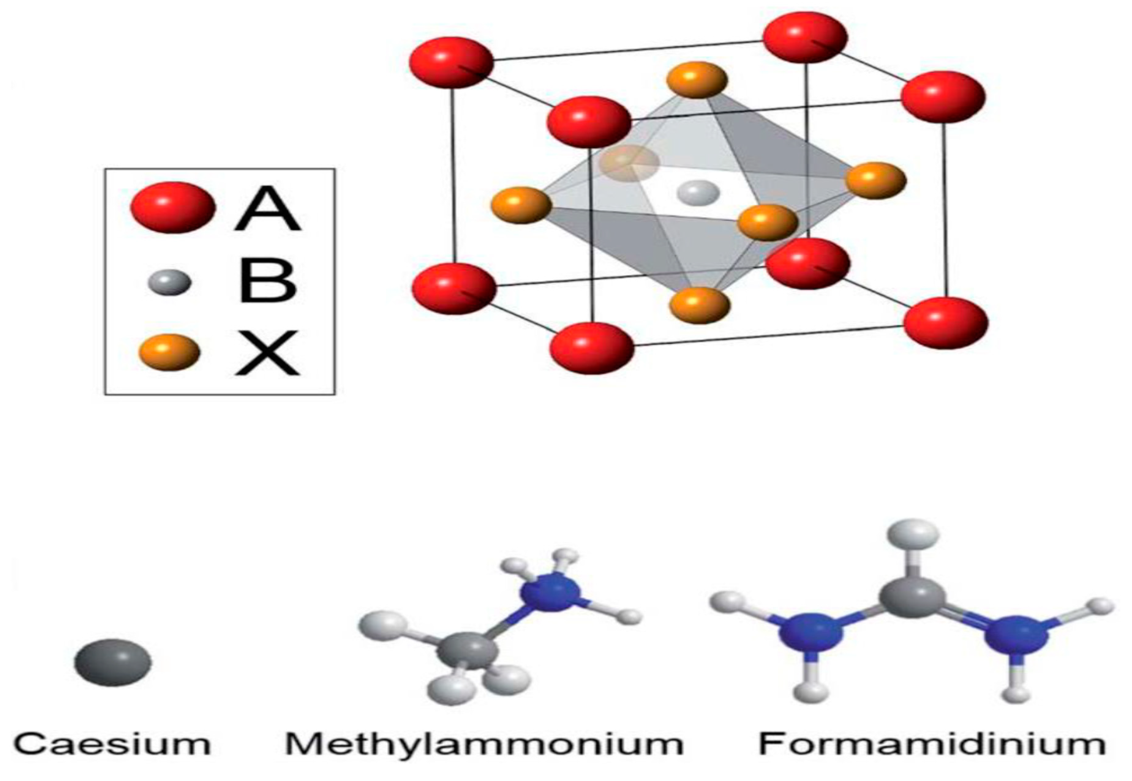
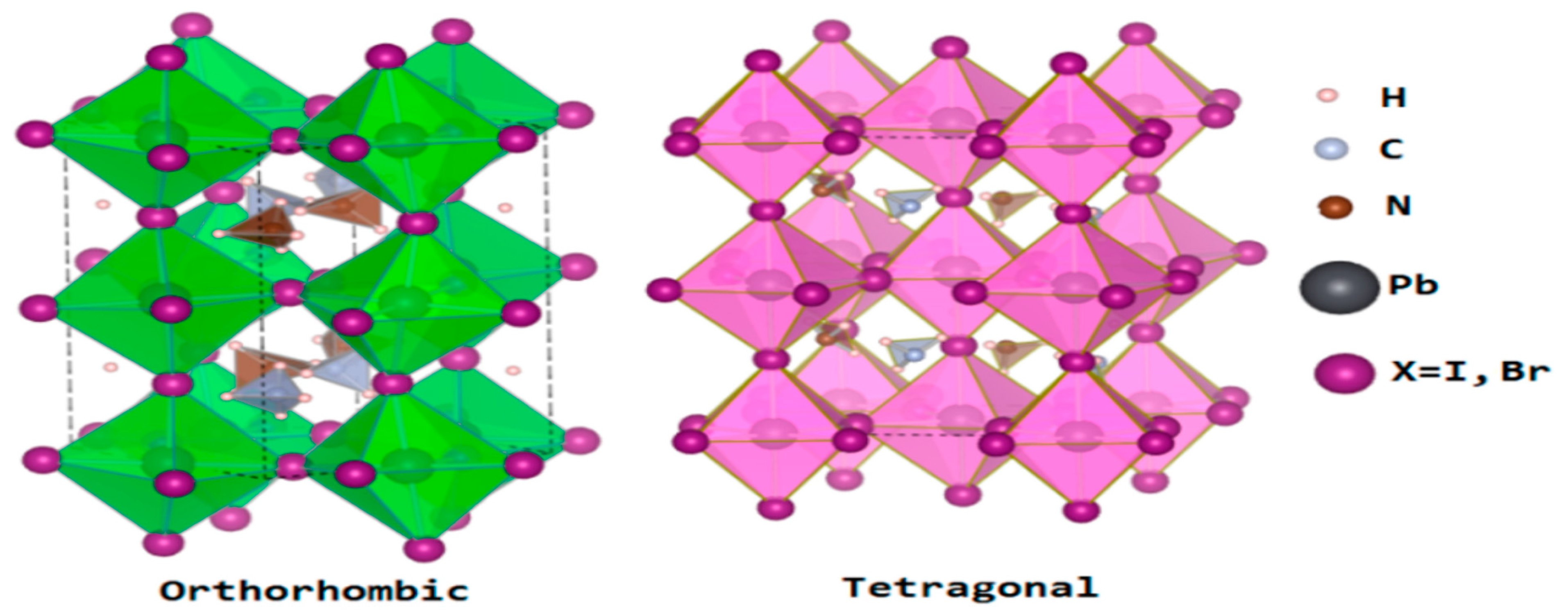
2. Single Perovskite Absorbers (ABX3)

The single perovskites are derived from the common formula of ABX3, whereby a monovalent is identified as A in the place of non-bonding positively charged ions, such as Cs, CH3NH3 or HC(NH2)2; a bivalent metal positively charged ion remains depicted as B for mainly Pb2+, Sn2+, Eu2+, Cu2+, Ge2+, etc.; and X represents a halogen negatively charged ion bonded to the strategically located metal, which is seen to include (F−, Cl− Br−, and I−). A perfect simple cubic crystal lattice is constructed by anionic 3D networks of corner-sharing (MX6/2) octahedra organo-metal halide perovskites, as shown in Figure 1. The self-assembly of the inorganic units is occupied by the monovalent cations which generate cuboctahedral cavities, including balancing the charge and indirectly dictating the long-range structural properties. To date, the A-sites with positively charged ions, including Cs, CH3NH3, or HC(NH2)2, are only capable of stabilizing 3D structures [51,52]. The narrow selection of A cations can establish the stabilization of 3D structure since the space of the inorganic composition can only keep hold of sizeable cations that are derived from the determinant tolerance factor [51]. From a structural standpoint, Sn and Ge are the only bivalent metal cations that can substitute for the toxic Pb2+ in single perovskites to form a three dimensional (3D) perovskite framework with properties of uniform values along all axes in, addition to displaying equivalent charge carrier transport features equally observed in the case of lead-based perovskites [27]. Therefore, Sn−and Ge−based perovskites are the two single perovskites that form a three dimensional (3D) perovskite framework. Herein, a summary of device performance on selected single perovskite light absorbers with general formula ABX3 based on 3D lead-free hybrid perovskite solar cells is displayed in Table 1.

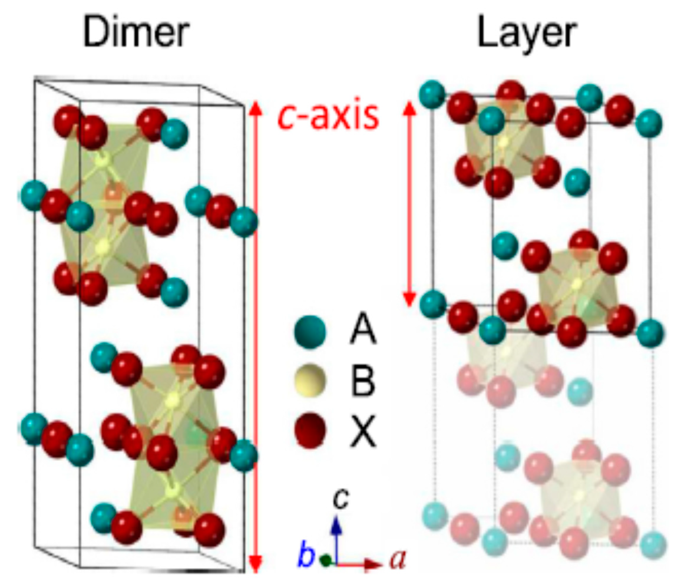
2.1. D ABX3 Metal Halide Perovskites and Perovskite-Related Absorbers with Diverse Dimensionalities

The crystallographic form of the 3D ABX3 organometal halide perovskites consists of corner-sharing BX6 octahedra with the A component neutralizing the overall charge, whereby the A component stands for organic positively charged ions, B represents the metal, and X halide negatively charged ions. The crystal structures of the 3D ABX3 organometal halide perovskites in the pristine phases and the atomic composition of the three A positively charged ions studied are as shown in Figure 2 [68].
At lower temperatures, the distortion of the BX6 having a B–X–B bond angle of 180 as well as ions in the interstices in regard to the 3D organometal halide perovskite lattice may be in orthorhombic phases. Hence, a function of temperature was found to cause the transition from orthorhombic to tetragonal to cubic perovskite structures. As a major function of temperature, the crystal structures of the 3D ABX3 organometal halide perovskites usually transit into the orthorhombic and tetragonal phases, as shown in Figure 3 [43]. These phase transitions can be influenced by various parameters, such as the precise stoichiometry of the perovskite or external limitations [69].
In the crystallographic form of the 3D ABX3 organometal halide perovskites, the A cation does not determine the band structure, but its magnitude is very crucial, whereby A being bigger or smaller could affect the expansion or contraction of the whole lattice. Moreover, the A cation appears to occupy charge neutrality within the lattice. Meanwhile, changing the B–X bond length is solely responsible for determining the bandgap. Based on the fact that a cation should appropriate amid the corner-sharing metal halide octahedra, a specific metal and halide must be known based on the fact that there exists a reasonably lesser magnitude range permitted for the A positively charged ions. Supposing A positively charged ions are extremely outsized, the 3D perovskite crystal becomes unsuitable, thereby leading to the formation of lower-dimensional layered perovskites, as shown in the Figure 4. On the other hand, in a situation where the A cation is too small, the lattice would be overly constrained to take shape [68].

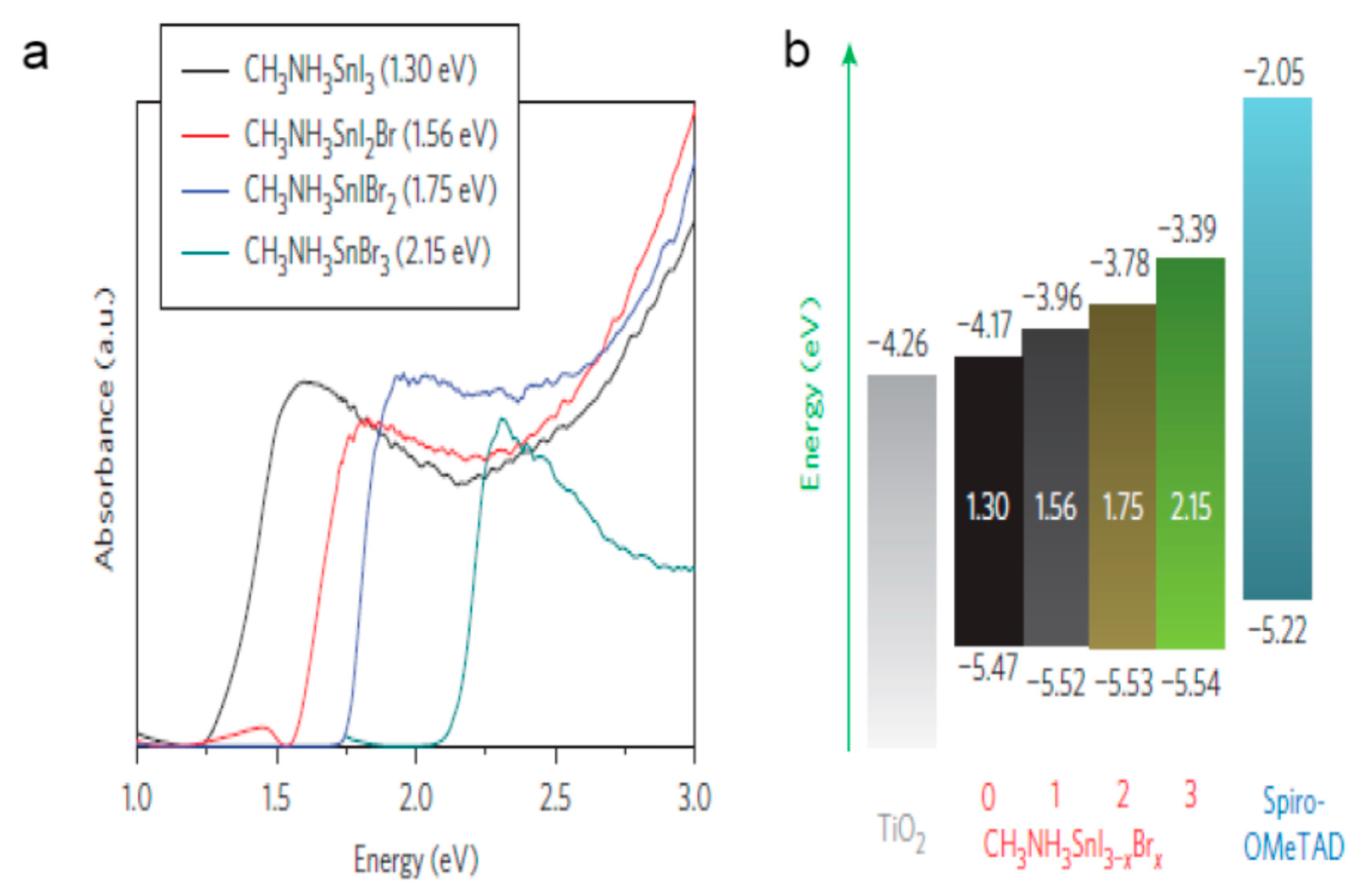
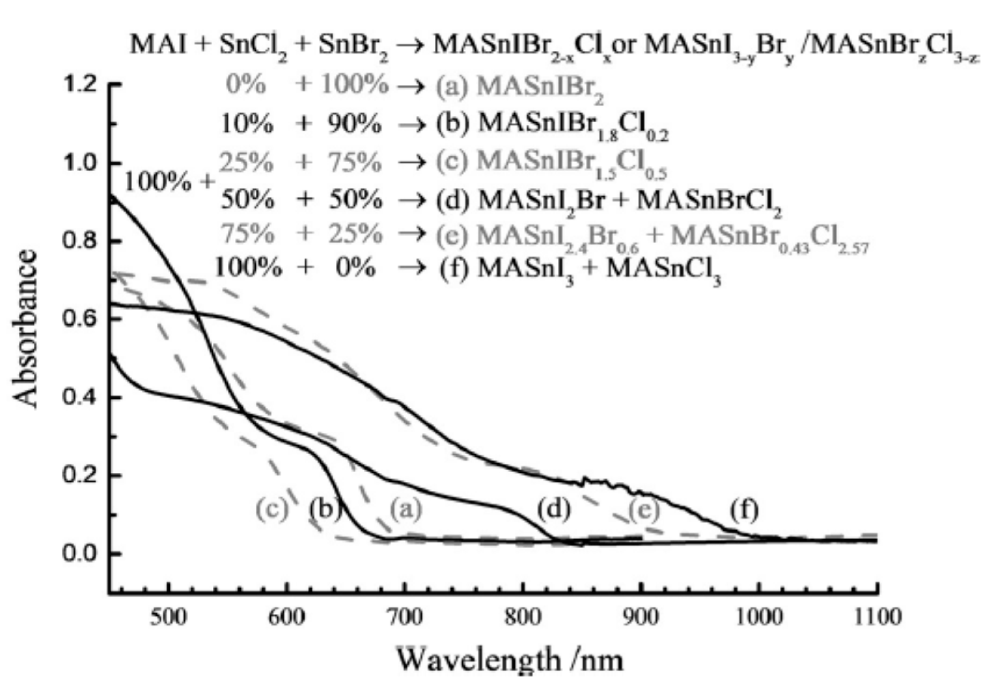
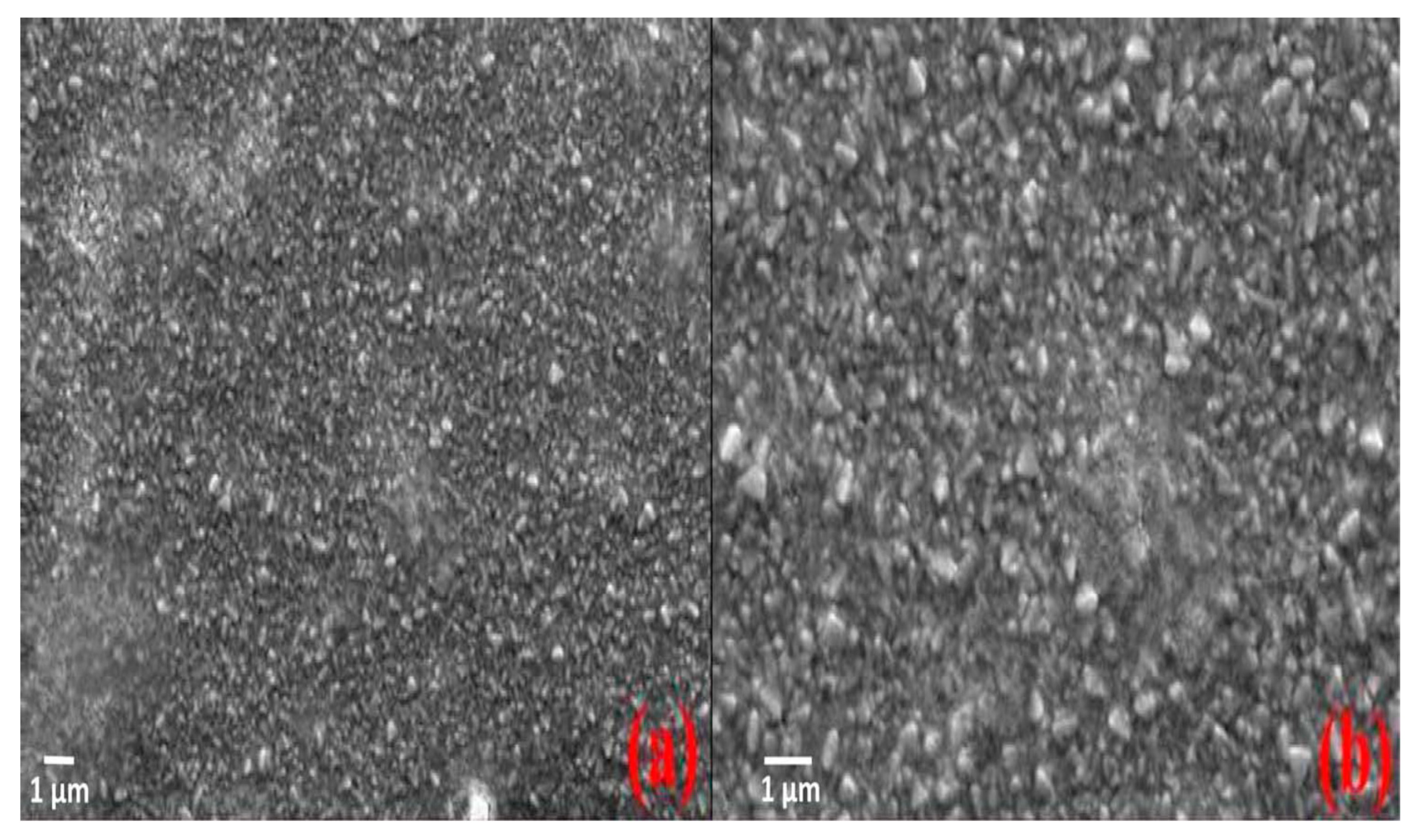
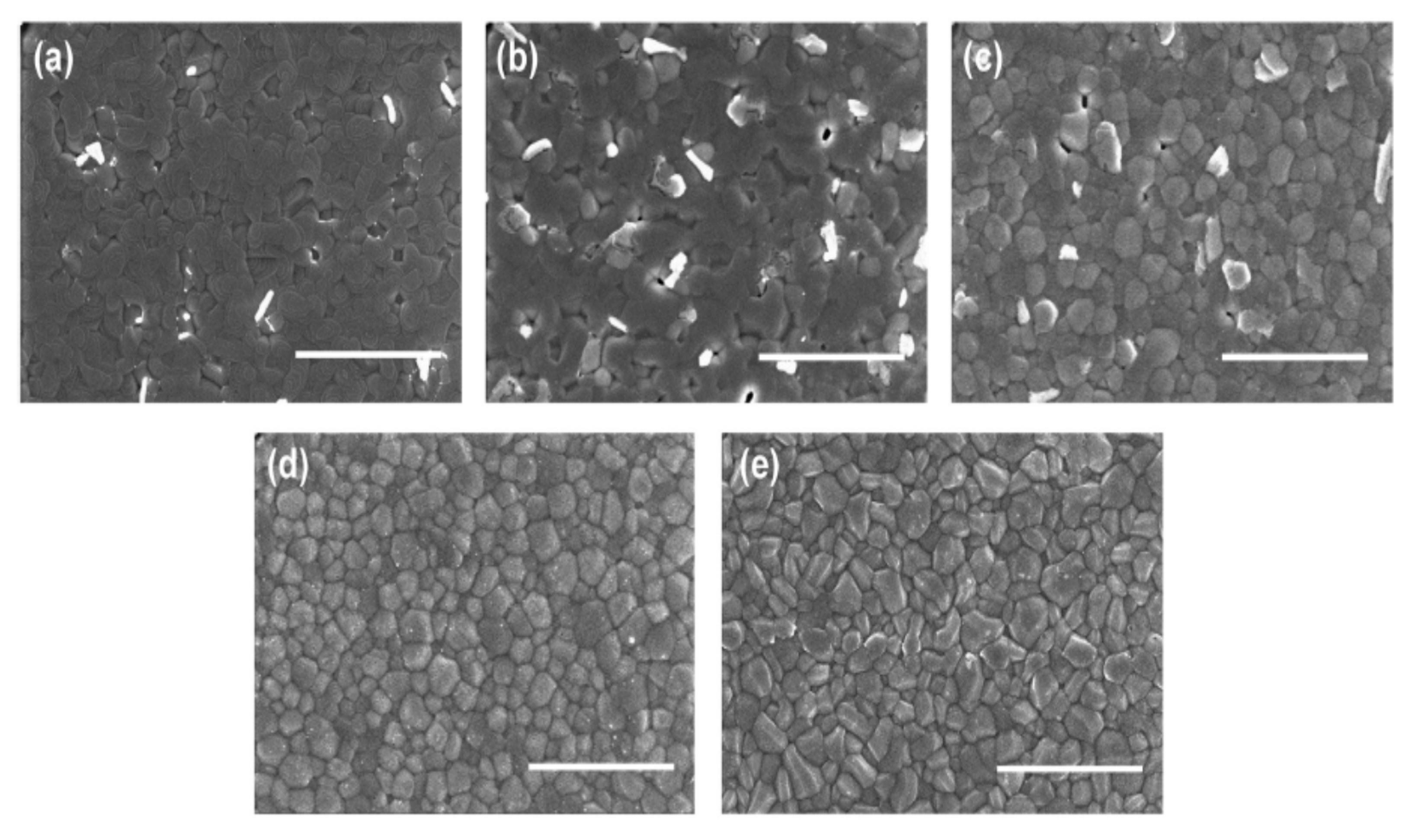
2.2. Sn-Based 3D Perovskite Absorbers (ASnX3)

Sn belongs to the carbon family of group IV in the periodic table of elements, and as a monoatomic ion, it has a radius of 110 pm. It is associated with a member of Pb (119 pm), which is composed to formulate the ASnX3 perovskite compound, where A stands for MA+, FA+, and Cs+ positively charged ions and X is a halogen negatively charged ions in analogy to APbX3 perovskite [72]. Noel et al. demonstrated the foremost CH3NH3SnI3 perovskite device administered on a mesoporous TiO2 framework. The compound had a bandgap of 1.23 eV. The devices obtained a voltage source of 0.88 V and yielded more than 6% efficiencies.
Nevertheless, the unstable nature of Sn-based compounds remains a challenge [73]. Hao et al. proceeded to report a lead-free solution administered solid-state photovoltaic device with CH3NH3SnI3 (methylammonium tin iodide) perovskite on organic an hole–transport layer spiro-OMeTAD coupled with mesoporous TiO2 support. The CH3NH3SnI3 perovskite material featured a bandgap of 1.3 eV. The devices achieved a voltage source of 0.68 V and yielded an efficiency of 5.23%. Furthermore, bandgap fixing was employed through chemical replacement in the procedure of the CH3NH3SnI3−xBrx solid solution, which remained manageably tailored to cover the visible wavelength region extensively. The CH3NH3SnI3−xBrx perovskite absorber featured a value of 1.75 eV optical bandgap. The solar devices obtained a voltage source of 0.82 V and yielded an efficiency of 5.73%. The open-circuit voltage experienced a tremendous improvement and was attributed to the rise in conduction bandgap by way of growing the Br substance inside CH3NH3SnI3−xBrx perovskite material, as shown in Figure 5 [54].
Furthermore, Tsai et al. reported the combination of MAI and the SnCl2/SnBr2 precursors in equal percentages with varied SnCl2/SnBr2 ratios—0/100, 10/90, 25/75, 50/50, 75/25, and 100/0 to form methylammonium (MA)-mixed tri-halide Sn perovskites, as shown in Figure 6. By starting with 0% SnCl2/100% SnBr2 ratios, the perovskite material of MASnIBr exhibited absorption at 700 nm by a bandgap of 1.81 eV. Through compounding the quantity of SnCl2 from 0% to 25%, the absorption experienced a blueshift, which gave rise to a bandgap with a value of 1.97 eV. Conversely, in the equal ratio of 50% SnCl2 /50% SnBr2, the absorption spectrum showed a major redshift equal to about 850 nm (Eg = 1.49 eV), further increasing the produced SnCl2/SnBr2 ratios and furthering the shifts of the spectra with its signal processing close to 1000 nm (Eg = 1.25 eV) at 100% SnCl2. The perovskite solar cell device with the proportionate composition of MASnIBr1.8Cl0.2 (SnCl2 = 10%) exhibited an outstanding device performance of 3.1% PCE, with a voltage source of 0.38 V, a photocurrent of 14.0 mA cm−2 and a 57.3% fill factor. Therefore, the experimental work gave credence to the fact that the insignificant amount of Cl within the trihalide perovskite material gave a superior performance of PSCs, which is generally due to the controlled charge recombination, the reduced charge build-up, and the improved exciton lifetime [55].
Recently, Tsarev et al. described the incomplete replacement of monovalent methylammonium (MA) positively charged ions by hydrazinium (HA) ions to enhance the stability of MASnI3 films as well as improve their morphology, thereby giving rise to notable build-up concerning the conversion efficiency of solar cell devices. The hydrazinium-loaded layer exhibited immeasurably exclusive stability upon exposure to light beneath an inactive air as likened to the source MASnI3 layers, which undertook instant transformation to MA2SnI6 based the operating conditions. The material photostability significantly improved due to the vigorous inhibition of Sn(II) disproportionation to Sn(IV) and Sn(0) by the incorporating hydrazinium ions. Furthermore, the incorporation of hydrazinium positively influenced the film morphology, whereby there was reduced denseness of holes and pinholes. Moreover, the photovoltaic output performance tremendously improved, whereby the solar cell efficiency increased by starting from 0% for MASnI3 to 2.6% for MA0.8 HA0.2SnI3 [56].
Meanwhile, Singh et al. implemented a series of experiments to study the comparative behavior of CH3NH3Cl powder and crystal as perovskite absorbers for photovoltaic application. The powder perovskite exhibited a bandgap of 2.5 eV, whereas the crystal perovskite showed a bandgap of 2.1 eV. The XRD and SEM result analysis showed structural characterization of perovskite absorber distribution at the titanium dioxide surface and was compared with easily accessible literature. The crystal pattern of the perovskite is confirmed from SEM. The solar device with a PEO-based solid polymer electrolyte obtained an open circuit voltage of over 0.48 V for powder perovskite and 0.60 V for crystal perovskite of CH3NH3SnCl3, while the yielded power conversion efficiency of 0.17% for powder perovskite and 0.55% for crystal perovskite of CH3NH3SnCl3 were recorded at 100 mW/cm2 (1 sun condition) processed in the ambient air surrounding. Therefore, the results show that the crystal perovskite is significantly superior to the powder perovskite of CH3NH3SnCl3, as displayed in Figure 7 [74].
By substituting the A cation of CH3NH3 with HC(NH2)2 cation, Koh and co-workers identified the FASnI3 perovskite film as a light harvester in a solar cell device, which achieved a bandgap with a value of 1.41 eV. By incorporating SnF2 on top of mesoporous TiO2, the solar device with the capping layer of FASnI3achieved a voltage source of 0.238 V as well as efficiency of 2.10% [57]. However, Zhang et al. (2016) reported bandgap engineering by chemical substitution, featuring the composition of FASnI2Br obtaining a bandgap with a value of 1.68 eV. By combining C60 by way of electron-transport coating and a MoOx film-based inorganic substance as a novel kind of free hole-transport coating with lead-free FASnI2Br perovskite, the perovskite of the Sn-based solar cell obtained a voltage source of 0.467 V and yielded an efficiency of 1.72% [75].
Moreover, Ke at al. demonstrated a novel kind of tin-centered perovskite absorber whereby ethylenediammonium (en) was incorporated into formamidinium (FA), resulting in the formation of new types of cavity 3D structures of {en}FASnI3 perovskite. It was observed that the incorporation of ethylenediammonium (en) into the A cation structure achieved an evident rise in the bandgap deprived of the necessities for solid solutions, material stableness, and enhanced photoelectric qualities of the formulated Sn-based absorbers. The superlative attainment of the 3D perovskite absorber by way of 10% en loading could be attributed to 1.5 eV as an ideal bandgap. Upon capping with an agent of {10% en} into the FASnI3 compound on a thin bedrock of poly[bis(4-phenyl)(2,4,6-trimethylphenyl) amine] (PTAA) as a hole-transporting layer as well as a 1 mm-thick substrate of mesoporous TiO2, the solar cell device obtained 7.14% PCE through a voltage source of 0.480 V, a photocurrent of 22.54 mA cm−2, and a fill factor of 65.96% [58]. On the other hand, Kayesh and co-workers demonstrated the incorporation of measured hydrazinium chloride (N2H5Cl) substance into an unmixed precursor solvent entity to formulate FASnI3 perovskite layers, which achieved a bandgap with a value of 1.37 eV. The outstanding incorporation of N2H5Cl resulted in decreased concentration of Sn4+ substance by 20% in the FASnI3 layer, thereby ensured the inhibition of the carrier recombination and the possibility to create pinhole-free uniform coverage on the substrates. The noteworthy enhancements reached in the Sn-based PSC coupled with FASnI3 film exhibited up to 5.4% power conversion efficiency and a major rise in the voltage source of 0.455 V [59].
Through varying the percentage of both contents, namely, formamidinium (FA) and methylammonium (MA) positively charged ions, Zhao et al. reported a tin-based hybrid compound of (FA)x(MA)1−xSnI3 (FA = NH2CH = NH2+, MA = CH3NH3+), which was designed with the aim of developing inverted perovskite fabricated devices. The bare MASnI3 film showed a more continuous distribution without significant traces of grain boundaries. As the content of FA was enhanced, the grain boundaries slowly became obvious, and the FASnI3 film showed crystal grains with sharp edges and clear boundaries. Some white grains were found in the films at lower FA content (x = 0.00, 0.25, and 0.50), which may be attributed to the phase partition caused by SnF2. These films also showed partial coverage through a small pinhole, which explained the low fill factor (FF) and the slightly lower average short-circuit current (Jsc) of their corresponding devices. However, the film morphology was greatly improved at higher FA contents (x = 0.75 and 1.00), which displayed whole coverage coupled with no obvious phase partition, thereby leading to superior system performance. The best performing (FA)0.75(MA)0.25SnI3 lead-free perovskite material obtained a bandgap of 1.33eV. The PSCs device with (FA)0.75(MA)0.25SnI3 through incorporating 10 mol% SnF2 additive exhibited 8.12% PCE and a better voltage of 0.61 V, which originated from better-quality pinhole-free perovskite layer morphology and hinders recombination activity in the system, as shown in Figure 8. Therefore, composition engineering of the requisite compound remains a unique technique for obtaining superior Voc along with PCE aimed at the stable performance of Sn-based perovskite solar cells [37].
Similarly, Gao and co-workers reported a structural regulation strategy through the insertion of cesium cation (Cs+) into the composition of FASnI3 for the formation of 3D Sn-faced lead-free CsxFA1−xSnI3. The inverted planar perovskite solar cell (PSC) constructed with Cs0.08FA0.92SnI3 showed 6.08% PCE and a significant voltage source of 0.44 V. Through their experimental and theoretical work, Gao et al. improved the spatial regularity, suppressed the loss of the electron in regard to Sn2+ and enhanced the thermodynamically structural solidity of FASnI3 by incorporating the Cs+ ion [60]. However, Shao et al. had a breakthrough in reporting a PCE as high as 9.0% through a voltage source of 0.525 V for formamidinium tin iodide (FASnI3) perovskite films featuring inside a planar p–i–n device assembly. The best performing perovskite films were synthesized by mixing both contents of a very little quantity (0.08 m) of 2D Sn-perovskite substrate and 0.92 m of 3D Sn-perovskite to induce top-quality crystallinity having distinct coordination of the 3D FASnI3 granules. The chemical platform for increased ordering and packing of crystal planes enhanced the toughness and reliability of the perovskite composition, which helped to restrain the configuration of tin vacancies and cause an overall background carrier density over the material. Thus, improved solar cell performance was a result of the great level of crystallinity and superior crystal coordination [61].
Using cesium (Cs) as the A cation in a 3D Sn-based perovskite, Chung et al. explained the synthesis of cesium tin iodide (CsSnI3) perovskite featuring 1.3 eV for the optical bandgap [76]. Moreover, Chen et al. demonstrated the preparation of CsSnI3, exhibiting an optical value of 1.3 eV as a bandgap. The Schottky solar cells with CsSnI3 obtained an efficiency value of 0.9% and a voltage source of 0.42V [77]. Subsequently, Kumar et al. illustrated the experiment of minimum temperature (70 °C) processed (CsSnI3) to develop solar cells exhibiting photocurrents beyond 22 mA/cm2 coupled with a spectral response increasing in the direction of 950 nm. The CsSnI3 perovskite possessed a value of 1.3 eV as an optical bandgap. Since CsSnI3 was being used as a photoabsorber, and with the ability to be disposed to form inherent defects linked with Sn cation vacancies that produce metallic conductivity, Kumar and co-workers demonstrated the inclusion of SnF2 as a stabilizer to control the metallic conductivity. The best performing CsSnI3 perovskite absorber with 20% SnF2 loading was observed upon its use on a solar device, producing a 2.02% PCE and 0.24 V as an open circuit voltage [62].
Besides, Sabba et al. rationalized the combination of various compositions of CsSnI3−xBrx by also specifically partially replacing bromine into bare CsSnI3 as a follow up to the previous report by Kumar and co-workers in a bid to further study the outcome of replacing bromine into the bare substance of CsSnI3 in the existence of SnF2. Amidst the different structures being synthesized, CsSnI2.9Br0.1 produced superlative performing results with a voltage source of 0.222 V, a photocurrent of 24.16 mA/cm2 as well as a fill factor with a value of 0.33, thereby indicating 1.76% conversion efficiency. By gradually replacing I with Br−, the perovskite absorber registered an increase in the optical bandgap through 38.5% alongside a blue shift in the absorption spectra. The favorable outcome of Br content inclusion for voltage enhancement was obvious for the CsSnI3 structure even in the absence of SnF2. The voltage enhancement was attributed to the reduction in Sn defects based on its missing atoms in its lattice sites, wherein it is revealed through the inferior carrier concentration or charge carrier densities of 1015 cm−3, as well as an extraordinary opposition to the mechanism of charge recombination in the instance of the Br-loaded CsSnI3−xBrx compound. The outstanding current densities were enhanced greatly due to the incorporation of SnF2 into the CsSnI3−xBrx compound [63].
Recently, Zhang et al. for the first time reported the chemical alloying substance, specifically, cobaltocene (by the formula of Co(C5H5)2), possessing an intense electron releasing ability as an additive to affect stability as well as influence the electrical property of the CsSnI3 perovskite substance for photovoltaic applications. Cobaltocene (Co(C5H5)2) is a commonly used one-electron reducing agent that can simply transfer an “extra” electron from the metal cobalt to form an 18-electron positively charged ion with great stableness. The CsSnI3 perovskite material is attributed to have chemical diversity and complex conformational space, proffering extremely promising adjustable composition in relation to chemical redox molecules. As a result of the outstanding attributes of the CsSnI3 perovskite material, an electron-rich environment provided by incorporating cobaltocene (Co(C5H5)2) offered the proficiency of inhibiting Sn2+ oxidization and reducing the trap density when compared to the plain CsSnI3. A solar cell device with the best performing CsSnI3 of 1% (Co(C5H5)2) loaded achieved a voltage source of 0.46 V and yielded a 3.0% conversion efficiency [64]. Therefore, the novel study provided an effective method for assembling active and steady solar cell devices by integrating donor elements to inhibit Sn2+ oxidation.
Conversely, Gupta et al. explained the synthesis of cesium tin bromide (CsSnBr3) perovskite material by way of an effective light harvester for the solar cells, exhibiting a direct bandgap with a value of 1.75 eV. The best performing solar cells with CsSnBr3 (with 20 mol% SnF2 additive) showed 2.1% conversion efficiency by way of JSC, a photocurrent of around 9 mA cm−2, a VOC source of 0.41 V, and fill factor with a value of 58% underneath 1 sun (100 mW cm−2) illumination when compared to the photovoltaic performance of solar cells with bare CsSnBr3. As stated earlier in previous sections, the addition of tin fluoride (SnF2) remained focused on the procurement of positive device operating results based on its primary function to counteract traps by way of occupying lattice spaces for the reduction of the surroundings carrier density. Therefore, it becomes clear that by way of appropriate encapsulation, Sn-based solar cells may grow into valuable mutually separate building blocks or as a part of larger cell structures [65].

2.3. Ge-Based 3D Perovskite Absorbers (AGeX3)

Ge belongs to the carbon family of group IV in the periodic table, similar to Sn and Pb elements. It is an element that is being studied to show potential responsibility for the actualization of perovskite solar cell applications. When compared to Pb2+, Ge2+ has the characteristics of greater electronegativity, a new covalent property, and an ionic radius (73 pm) seen to be lesser than that of Pb (119 pm). Theoretical studies have attested to the potency of using germanium halide perovskites for solar cell applications, but they have been rarely investigated experimentally. Based on theoretical and experimental studies, Stoumpos et al. reported the effects of the mixed organic/inorganic germanium perovskite materials with formula AGeI3 (A = Cs, organic cation) experimentally. Through CsGeI3 as the model composition, the following 3D compounds were prepared: methylammonium (CH3NH3GeI3), formamidinium (HC(NH2)2GeI3), acetamidinium (CH3C(NH2)2GeI3), and guanidinium (C(NH2)3GeI3). The 3D perovskite materials exhibited direct bandgaps of 1.6 eV for CH3NH3GeI3, 1.9 eV for HC(NH2)2GeI3, 2.2 eV for CH3C(NH2)2GeI3, and 2.5 eV for C(NH2)3GeI3. Based on structural grounds, the consequences of Cs substitution with larger cations of the organic compounds will activate the stereochemical representation of the 4s2 “inert pair” (likewise known as lone pair activation) which thereby activates the alteration of the band formation, resulting in a great enlarging of the bandgap [78].
Furthermore, Krishnamoorthy et al. synthesized three halide perovskite compounds with the formulation of AGeI3 (A=Cs, CH3NH3, or HC(NH2)2). The compounds remained stable until 150 °C, and possess bandgaps linked to the A-site positively charged ion size. The bandgaps exhibited by the materials were 1.63, 2.0, and 2.35 eV for CsGeI3, MAGeI3, and FAGeI3, respectively. CsGeI3 and MAGeI3 were observed to have relatively smooth morphology, while that of FAGeI3 was very poor. Thus, the device-fabricated solar cells with the germanium iodide perovskites of both CsGeI3 and MAGeI3 using compact and mesoporous TiO2 and Spiro-OMeTAD as electron- and hole-selective contacts exhibited a PCE of 0.11% and a voltage source of 0.074 V for CsGeI3 as well as a 0.20% PCE and voltage source of 0.15 V for MAGeI3.
Based on the poor film quality of FAGeI3, solar cells did not show any photoelectric properties. The poor performance of the devices could be attributed to Ge4+ formation by oxidation. Overall, the study showed a strong potential for Ge-based halide perovskite compounds in photovoltaic applications [66]. Recently, Kopacic et al. explained the synthesis of germanium halide perovskites from GeI2, MAI, and MABr, respectively, by using DMF as a solvent for the precursor solution. Kopacic et al. showed that chemical composition plays a crucial role in improving material stability and performing capacity of the germanium perovskite compounds when adapted to function in a fabricated solar cell. Hence, Kopacic et al. observed excellent material stability and unique operating capacity through chemical composition by incorporating bromide ions into the matrix of methylammonium germanium iodide perovskite. The planar p–i–n solar cells with the best-performing MAGeI2.7Br0.3 obtained a value of 0.57% PCE. Based on this study, it was shown that the bromide substance in methylammonium germanium halide perovskites shows a key function in the performance of the photovoltaic devices [67].

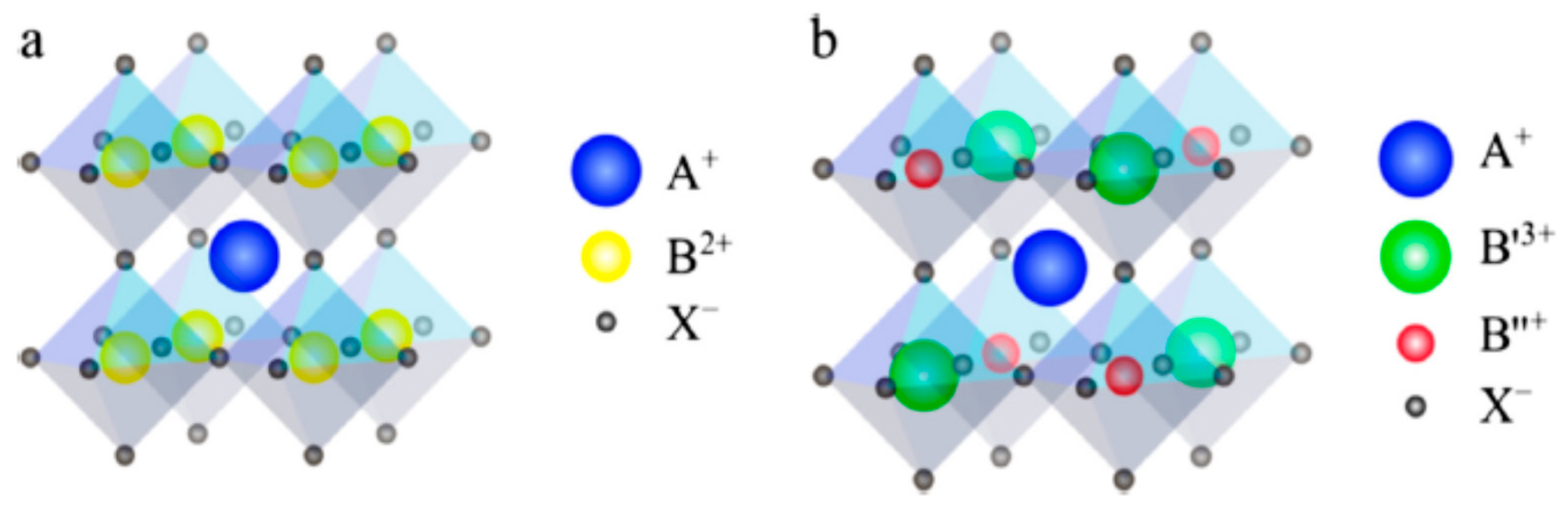
3. Double Perovskite Absorbers (A2BB′X6)

The double perovskite, converted to a quaternary AI2BIBIIIX6 formula, is a neighboring derivative of the ABX3 single hybrid halide perovskites. Their derivatives are composed of metallic halide octahedra BIX6 or BIIIX6 units that assign intersections among six adjacent octahedra having dissimilar ions to develop 3D lattice, as shown in Figure 9. The monovalent and trivalent metal ions coexisting together are enshrined in the crystal composition of a standard double perovskite. The two distinct monovalent and trivalent metal ions that periodically substitute for the toxic Pb2+ in a single perovskite have copious elementary combinations that furnish extensive alternatives aimed at achieving preferred qualities [79]. Herein, a summary of device performance on selected metal halide double perovskite solar cells is listed in Table 2. Meanwhile, an overview of metal halide double perovskite on their material compositions, bandgaps, and morphological properties alongside synthetic methods is listed in Table 3.
Due to the investigation for more lead-free perovskite materials, a novel class of double perovskite materials has been produced. Slavney and coworkers replaced Ag+ and Bi3+ for toxic Pb2+ taken with the perovskite network in Cs2AgBiBr6. The perovskite material showed a direct bandgap value of 1.95 eV as well as basic photoluminescence life of about 660 ns, which is suited for photovoltaic applications. The photoluminescence (PL) decay curve of Cs2AgBiBr6 showed a great defect tolerance based on the contrast involving single crystal and powder. Moreover, it showed superfluous heat and moisture stability when likened to (MA)PbI3 [94]. McClure et al. reported the preparation of Cs2AgBiBr6 and Cs2AgBiCl6 double perovskites through both the solid and synthetic solution pathways. The relative diffuse reflectance measurements showed bandgaps with a value of 2.19 eV for Cs2AgBiBr6 and a bandgap with a value of 2.77 eV for Cs2AgBiCl6. The density of state calculation for the bandgap indicated that transition from the valance to the conduction band takes place from the occupied halogen 3p/4p orbitals to antibonding Ag 5s and Bi 6p orbitals. The presence of the Ag 4d orbitals reduces the bandgap and interacts with the notable field of 3p/4p orbitals situated in the halide ion to ensure modification of the valance band, thereby producing an indirect bandgap. The two composites are stable once opened to the atmosphere [95].
Through theoretical study and experimental synthesis, Volonakis et al. reported photosensitive features in the group of double perovskite A2B′B″X6 with A = Cs, B′ = Bi, Sb, B″ = Cu, Ag, Au and X = Cl, Br, I. Theoretical study envisaged that all hybrids possess indirect bandgaps coupled with the projected approach for tuning them into direct bandgaps. Furthermore, the double perovskite of Cs2AgBiCl6 was successfully synthesized, and it was shown to belong to the fm3m space assembly and consist of BiCl6 and AgCl6 octahedra, which are fluctuating in a rock-salt-face-centered structure. The hybrid revealed an indirect bandgap with a value of 2.2 eV [85]. Greul et al. synthesized and reported Cs2AgBiBr6 film being annealed at 250 °C with a 2.5% conversion efficiency and a voltage source surpassing 1 V. This stands presently as the maximum recorded voltage source for bismuth halide perovskite materials, thereby serving as a potential light-absorbing double perovskite material [96].
Even though halide double perovskites have gained attention due to their composition of lesser toxicity elements, stability in the air, and long carrier life, there are still challenges most double perovskites, including Cs2AgBiBr6, have faced due to their wide bandgaps that limit photoconversion efficiencies. Hence, Li et al., through a solution-based route, effectively synthesized phase-pure Cs2AgSbBr6 thin films, as well as Cs2Ag(SbxBi1−x)Br6 with the mixing alloys of parameter x continuously changing over the complete composition extent (x between 0.5 and 0.9). Through this novel route, Li et al. reduced the 2.25 eV bandgap of Cs2AgBiBr6 and 2.18 eV of Cs2AgSbBr6 to as low as 2.08 eV of Cs2Ag(SbxBi1−x)Br, thereby proving the fittingness of double perovskites for photovoltaic and photocatalytic applications [86]. By way of implementing a crystal engineering approach which offered to transform the standard double perovskites of Cs2AgBiBr6 by simply influencing the gradual crystal change in temperature and speed, Klarbring et al. attained the minimum disclosed bandgap of lead-free double perovskite Cs2AgBiBr6 to appreciably drop in bandgap value by around 0.26 eV, thereby attaining the lowest described bandgap of 1.72 eV for Cs2AgBiBr6 in ambient settings, whereby bandgap reduction was validated by both electronic absorption and photoluminescence magnitudes [87].
Due to the morphology engineering of Cs2AgBiBr6, Gao and co-workers focused on improving the film-forming ability of the perovskite, because it is known that perovskite film with high surface coverage and less defects is influential to the rapid transportation of both electrons and holes, including having an evident effect on device stability and best performing ability [81,97]. Hence, the results showed Cs2AgBiBr6 film morphology with granules composed of quality crystals that were obtained via the method of anti-solvent treatment annealed at high temperatures, thereby exhibiting an indirect bandgap value of 1.91 eV. Conversion efficiency with a value of 2.2%, a voltage source of 1.01 V, a photocurrent of 3.19 mA/cm2 and a fill factor with a value of 69.2% were exhibited via an inverted planar heterojunction solar cell device with a Cs2AgBiBr6 layer. The device established material stability with no hysteresis [81]. Meanwhile, Wu et al. reported 1.44% power conversion efficiency with a voltage source of 1.04 V, a photocurrent of 1.78 mA/cm2, and a fill factor with a value of 78%, as attained in the Cs2AgBiBr6 film being annealed at 250 °C [98]. More importantly, the film shows superior thermal and ambient stability, thereby revealing the potential for lead-free perovskite solar cells. The figure shows SEM and XRD spectra. SEM of Cs2AgBiBr6 film annealed at 250 °C shows smooth morphology which influenced the rapid transportation of both electrons and holes [81]. Using the first planar structure solar device based on double perovskite Cs2AgBiBr6, Ning et al. demonstrated, by preparing Cs2AgBiBr6 layers that are made of high-level crystal property granules with diameters equivalent to the layer texture, a reduction in the granule periphery length and carrier recombination. The Cs2AgBiBr6 layers show elongated electron–hole diffusion lengths of more than 100 nm, thereby supporting the assembly of planar construction double perovskite solar cells. The resultant solar cells built on planar TiO2 exhibited over 1% typical power conversion efficiency [99].
Bandgap engineering provides an important technique for narrowing the large indirect bandgap, thereby targeting photovoltaic performance. Using Cs2AgBiBr6 as a high-value target compound, bandgap engineering through alloying InIII/SbIII of has been duly recorded. Du et al. reported the fixing of bandgaps concerning Cs2Ag(Bi1−xMx) Br6 (M = InIII/SbIII) by introducing InIII/SbIII to take up to 75% of InIII, which resulted in an enlarged bandgap equal to 37.5% SbIII with a diminished bandgap, thereby supporting bandgap modulation of about 0.41 eV throughout the incorporation of the dual metals through a minimum 1.8 eV bandgap on behalf of Cs2Ag(Bi1−x Mx)Br6. The different atomic configurations for the two metals (In/Sb) are responsible for the difference in bandgaps shifting directions [100]. Meanwhile, Liu et al. demonstrated bandgap tailoring of Cs2AgBiBr6 by incorporating only Sb to replace 75% content of Bi by the use of a solution-processed approach in a solvent medium of dimethyl sulfoxide at 180 °C. The Sb substitution drastically reduced the bandgap of Cs2Ag(SbxBi1−x)Br6 at a value of 2.22 eV when x = 0 to a value of 1.97 eV when x = 0.75. The effective bandgap reduction through the simple solution might speed up the enhancement of Cs2AgBiBr6 double perovskite for photovoltaic applications [101].
Furthermore, Wei and co-workers described the preparation of double perovskite Cs2AgSbBr6 with the aim of evaluating and maximizing its utilization. Using hydrothermal methods, a black Cs2AgSbBr6 was successfully prepared with a value of 1.64 eV to support a low bandgap. However, the compound experienced a color change from black to brown due to the occurrence of charge transfers from Sb3+ to Sb5+. A working device with Cs2AgSbBr6 as a solar absorber on fluorine-doped tin oxide (FTO)/TiO2/perovskites/spiroOMeTAD/Au architecture was fabricated and exhibited a 0.01% efficiency, a voltage source of 353.29 mV, a short circuit current of 0.08 mA cm−2 and a fill factor with a value of 35.9% on perfect films without antisolvent preparation [88]
Through the rich substitutional chemistry attributes of hybrid lead-free halide double perovskite for providing novel classes of perovskite materials [99], Volonakis, et al. reported bandgap engineering via compositional engineering of Cs2AgBiBr6 by introducing In and Cl or Br to substitute for Bi and Br, respectively, to achieve both double perovskites of Cs2AgInCl6 and Cs2AgInBr6. The double perovskite of Cs2AgInCl6 attained a successful synthetic outcome through a measured 3.3 eV bandgap, and X-ray diffraction produced a configuration with the space group Fm3m. Hence, the synthesis of mixed halides has created more possibilities intended for the growth of double perovskite and tunable bandgaps [102]. Meanwhile, Zhou et al. designed and reported bandgap engineering via compositional fixing of Cs2AgBiBr6 by presenting In and Cl to replace Bi and Br, respectively. Due to the design for hydrothermal synthesis of Cs2AgInCl6 in regard to the growth of single crystals, the perovskite material crystallized Cs2AgInCl6 into a single crystal via the chemical composition of alternating octahedra of [AgCl6] and [InCl6] in the salt composition. Cs2AgInCl6 experimentally obtained a 3.23 eV direct bandgap and theoretically obtained a 3.33 eV bandgap [103]. Besides, the perovskite material showed exceptional moisture, light, and heat stability, which indicates a huge possibility for photovoltaic application through further bandgap engineering [102]. Dahl et al. carried out the preparation of nanocrystals of Cs2AgInCl6 and Cs2AgSbCl6 using the colloidal preparation technique of introducing acyl halides within the ambient of the surrounding temperatures. The two compounds displayed bandgaps wherein Cs2AgSbCl6 showed a value of 2.57 ± 0.05 eV as an indirect bandgap, and Cs2AgInCl6 displayed a value of 3.57 ± 0.03 eV for a direct bandgap. Based on degradation assessment, Cs2AgInCl6 showed a decrease in material stability over Cs2AgBiCl6 to Cs2AgSbCl6 [90]. However, Zhou et al. utilized the colloidal preparation technique through a modified one-pot hot injection system to prepare a Cu(I)−Sb-based double perovskite nanocrystal of (Cs2CuSbCl6 NCs) with the smallest bandgap of 1.66 eV when compared to other lead-free double perovskites nanocrystals. Due to the compound’s unique stability to ambient air, the outstanding properties of the compound could make it a suitable light-absorbing material for photovoltaic utilization [91].
However, Karmakar et al. reported bandgap engineering via the compositional engineering of Cs2AgBiBr6. By incorporating Sb and Cl to replace Bi and Br, respectively, with doping of Cu2+, Cs2SbAgCl6 was formed, whereby the perovskite materials exhibited an effective shift in their bands from around a value of 2.6 eV (parent Cs2SbAgCl6) to around a value of 1 eV (Cu2+-doped Cs2SbAgCl6). The patterns of XRD for the Cu2+-doped Cs2SbAgCl6 polycrystalline materials indicated an extended range of crystallinity through non-uniform microstrain in the crystal lattice. The perovskite materials indicated thermal and moisture stability based on a comprehensive stress analysis that was conducted on the material for 365 days [82]. However, Zhang et al. designed and reported bandgap fixing for Cs2AgBiBr6 by presenting Na and I to replace Ag and Br, respectively, thereby giving rise to new and extremely stable Cs2NaBiI6 compounds. The new material has a value of 1.66 eV for a low bandgap and exhibited high stability when exposed to the surrounding air. The fabricated device constructed on Cs2NaBiI6 exhibited 0.42% conversion efficiency with a voltage source of 0.47 V, a photocurrent value of JSC = 1.99 mA/cm2, and a 44% fill factor, while the fabricated Cs2NaBiI6 as light absorber film revealed great stableness and reproducibility [104]. Moreover, Peedikakkandy et al. analyzed the fact that the compound Cs3Bi2I9 of iodobismuth ternary perovskites has recorded some achievements, but a wide bandgap and lower structure dimensions are its visible limitations. As such, Peedikakkandy et al. altered the broad bandgap of Cs3Bi2I9 composition to a small bandgap of double perovskite of Cs2NaBiI6 by Na2S inclusion, thereby presenting a near-to-finest bandgap of ∼1.5 eV. The sodium ion in Na2S plays a major role in replacing a trivalent bismuth ion of the Cs3Bi2I9 composition and forces the conversion to a double perovskite formation of (Cs2NaBiI6), while the divalent sulfur ion tends to occupy the crystal voids and tailor the bandgap. The XRD analysis of the altered Cs2NaBiI6 showed a great level of crystallinity, thereby giving a suitable morphology to support the utilization of its films for solar cell devices [92]. Alternatively, Cao et al. used the solid-state reaction method and the hydrothermal method by incorporating VCl3 as the vanadium source to prepare a red crystal halide double perovskite of Cs2NaVCl6 by way of reaching a bandgap with a value of 2.64 eV. Moreover, the material exhibited extraordinary attributes by showcasing two-fold strong absorption bands at 558 and 900 nm, which can be considered for photosensitization [89].
The introduction of gold as an element into the composition of double perovskites is of paramount importance due to its electronic properties. For the preparation of mixed gold halide double perovskites, Ghosh et al. utilized a solution-processed route to produce a tetragonal crystal of (MA)2Au2X6, (X = Br, I) double perovskites with an ideal bandgap of around 1.0 eV less than traditional halide-oriented compounds of double perovskites. Even though the compound was found to be hygroscopic, its single crystals and the thin film showed no degradation, thereby indicating superior material stability. The double perovskite showed photoresponse joined by small confined density, thereby indicating its possibility in PV utilization [93].

Ordered-Vacancy Double Perovskite Absorbers (A2BX6)

Ordered-vacancy double perovskites converted to the typical formula (A2BX6) are close derivatives of the ABX3 single metal halide perovskites, whereby their derivatives are constituted of a face-centered network of closely secluded [BX6] components through A-site cations inhabiting the cuboctahedral spaces [22,109]. Due to the quest for the production of chemical compositions meant for solar cell deployment, Lee et al. introduced a new group of atomic iodosalt compositions of Cs2SnI6 whereby Sn stays as a cutting edge with +4 oxidation state, thus fashioning the material to be stable in atmospheric conditions. Using Cs2SnI6 as a hole-transporting agent, a mesoporous TiO2 film dye-sensitized solar cell (DSSC) was successfully fabricated in ambient air, which delivered 4.7% of power conversion efficiency [110].
Furthermore, to overcome the synthetic challenges in solution processing of Cs2SnI6 and to boost optimal material performance, Lee et al. established a two-step solution technique. In step 1, a pure crystal-like layer was produced with the aid of SnI solution, while in step 2, a new series of Cs2SnI6−xBrx films was established on comprehensive structural, electrical, and optical analysis. These air-steady molecular semiconducting iodosalts of Cs2SnI6−xBrx provide values of around 1.2 eV to 2.9 eV as the desired bandgaps within the range of x where x < 3. By employing the solar cell device with Cs2SnI6−xBrx films, it showed a 2.1% power conversion efficiency based on the case where x = 2 of the requisite compound [83]. However, Saparoy et al. developed and reported a vacuum-based deposition technique aimed at synthesizing a single-phase film of Cs2SnI6, wherein it yielded a 1.6 eV direct bandgap. Cs2SnI6 was used for all fabrication processes in the air-surrounding environment, indicating a promising future of inexpensive, clean, safe, and stable solar cell productions [111]. Using the hydrothermal method, Han and co-workers demonstrated the formulation of a double perovskite devoid of lead such as Cs2SnX6 (X = I and Br) powders. As one of the constitute of the perovskites, half of the Sn locations are occupied by vacancies and maintain their 4+ oxidation state. The bandgaps of Cs2SnI6 and Cs2SnBr6 were established to be 1.84 and 1.42 eV, respectively, thereby showcasing these perovskites as futuristic-based perovskites for PV utilization [105].
Furthermore, Karim et al. prepared solid solutions of mixed A2SnX6 compounds to study their photophysical and electronic attributes, whereby Cs2SnCl6, Cs2SnBr6, and Cs2SnI6 exhibited optical bandgaps with values of around 4.89 eV, 3.23, and 1.35 eV, respectively [106]. Meanwhile, Schwartz et al. demonstrated the preparation of Cs2PtI6 crystal composition with a bandgap value of 1.4 eV. An assembly of planar superstrate n–i–p solar cells administered with the configuration of F: SnO2/CdS/ Cs2PtI6/carbon/Cu showed an efficiency of 13.88% with low Voc shortfall [107].
Despite the isolated octahedral units, ordered-vacancy double perovskite Cs2SnI6 has recently been studied for photovoltaic application due to the space-efficient composition of the iodide network that delivers electronic distribution. Maughan et al. furthered this research by using the solid solution method to prepare Cs2SnI6 from the formulation of Cs2Sn1−xTexI6, and by substitution of tin with tellurium the compound Cs2TeI6 perovskite was formed. The Cs2SnI6 perovskite material exhibited a 1.25 eV optical bandgap, whereas Cs2TeI6 displayed a 1.59 eV optical bandgap. However, the existence of exciton-like attributes close to the absorption threshold ascending from the Te(IV) 5s2 electron made the establishment of the optical gap for Cs2TeI6 problematic. The tightly packed anionic network and the interface concerning the B-site ions and the halide within these materials are solely responsible for their general structure−property relationships. The arrangement and uniformity of the conduction band due to the valence bands that are held by the I 5p orbitals have caused major variation concerning the electronic peak compositions of Cs2SnI6 and Cs2TeI6.
Moreover, the intensification in the covalent bonds of the [TeI6] octahedral constituents corresponding to that of [SnI6] was due to the enlarged Pauling electronegativity of Te4+ (χ = 2.1) correlated to that of Sn4+ (χ = 1.8). However, there was no measurable PL intensity on cold-pressed polycrystalline pellets of Cs2SnI6 and Cs2TeI6. From the findings, experimental investigation offers a background view to comprehend composition−property interactions of cutting-edge light-harvesting compounds [109].
For this reason, that lattice dynamics and structural instabilities strongly control the electronic properties of double perovskite halide semiconductors. Maughan et al. further studied the Rb2SnI6 vacancy-ordered double perovskite. By substituting Cs+ ion with the lesser Rb+ ion inside the Cs2SnI6 compound, the formation of Rb2SnI6 was accompanied by tremendous changes in structural and electronic behavior. Based on synchrotron powder diffraction analysis, Rb2SnI6 took on the tetragonal lattice with omitted Sn ions or atoms that were orderly arranged in the double perovskite composition at ambient temperature and went through a stage conversion to a lower-symmetry monoclinic configuration when cooled, being identified through collective octahedral slanting of the [SnI6] octahedra. At all given temperatures, the studies on X-ray and the neutron pair scattering function suggested that the confined complex surroundings of Rb2SnI6 were coherent with monoclinic composition. This finding may well be justified from the bond valence study, which indicated that Rb+ ion bonding is enhanced in the monoclinic composition. However, this was not so in the case of Cs2SnI6, in that at all given temperatures take on the cubic vacancy-ordered double perovskite compositions [22].
Based on the solution-processed approach being supported by reaction mixture oxidation of Pd2+ to Pd4+, Sakai and co-workers reported a new-type of lead-free material, i.e., hexabromopalladate(IV) (Cs2PdBr6). The Cs2PdBr6 formed into a cubic network with the space group Fm3m, providing evidence of unique composition and chemical stability. The optical analysis confirmed that the multi-layered structure exhibited a bandgap value of 1.6 eV. Cs2PdBr6 showed a photoresponse based on an assembly of indium tin oxide (ITO)/Cs2PdBr6/Ag, thereby indicating its suitability for utilization in optoelectronic and photovoltaic applications [112]. Meanwhile, Chen and co-workers operated a two-step vapor deposition technique for the formation of titanium-based vacancy-ordered halide double perovskites, such as the synthesis of cesium titanium(IV) bromide (Cs2TiBr6). The Cs2TiBr6 films showed a favorable bandgap value of 1.8 eV, elongated and well-adjusted carrier diffusion lengths greater than 100 nm, appropriate energy levels, and environmental stability. Cs2TiBr6 thin films of a perovskite solar cell device exhibited power conversion efficiency with a value of 3.3%. By alloying with iodide or chlorine, it was foreseen that composition engineering of Cs2TiBr6 thin films would provide a group of titanium-based double halide perovskites along with a controlled bandgap and properties for a wide range of optoelectronic applications [108].
Ju et al. experimentally prepared a family of titanium-based ordered-vacancy double halide perovskites through composition engineering by alloying with iodide or chlorine of Cs2TiBr6 thin films. Following a sequence (x = 0, 2, 4, 6) of Cs2TiIxBr6−x, Cs2TiI6 and Cs2TiBr6, as end members, they were synthesized through the melt-crystallization method. Based on optical analysis, the prototypical members of the Ti-based perovskite extraction processes such as Cs2TiIxBr6−x showed tailored bandgaps linked to the 1.38 and 1.78 eV standard values for photovoltaic applications. In particular, the measured values of around ∼1.02 and ∼1.78 eV of optical bandgaps were exhibited by phase-pure Cs2TiI6 and Cs2TiBr6, respectively; whereby the measurements were compared to a measured value of ∼1.51 eV for the optical bandgap of MAPbI3. These newly synthesized Ti-based double perovskites demonstrated stability and processability, thereby confirming the potential of their usage in PSCs. It was foreseen that further exploration of the Ti-based double perovskite family using the solution/vapor processing approach and material/device engineering would yield the benefits of having energy-saving, non-hazardous, inherently/ecologically stable, and low-cost perovskite solar cells [113].
Other sets of vacancy-ordered double perovskites are the tellurium-centered double perovskites. Ju and co-workers reported a family of Te-based lead-free perovskite A2TeX6 (A = MA, FA or BA; X = Br− or I−, MA = CH3NH3; FA = CH(NH2)2; BA = benzylamine) as potentially active materials for optoelectronic devices. These perovskites exhibited broad absorption (812–871 nm). Ideally, light-harvesting of up to 800 nm (the near-infra (NIR) region) of materials is preferable as light absorbers for potential applications in plain and simple solar cells, including NIR photodetectors. Moreover, the perovskite materials exhibited a tailoring bandgap (1.42–2.02 eV), a small trap density (∼1010 cm−3), and high mobility (∼65 cm2 V−1 s−1). MA2TeBr6, one of the members of the Te-centered double perovskite and with a bandgap of 2.00 eV, showed an encouraging result, with the aim of possessing a long carrier lifetime of ∼6 μs and a corresponding carrier diffusion length of ∼38 μm, which are ideal compounds for solar cells. Moreover, the perovskite compounds were found to be robust at ambient conditions, being stable for at least two months without showing any sign of phase change [114]. Hence, a summary of the ordered-vacancy double perovskites with their synthetic methods has been listed in Table 4.

4. Two-Dimensional (2D) Perovskite Absorbers

Two-dimensional (2D) perovskites, which are hybrid perovskites with low dimensionality, have received wide attention in the field of photovoltaics [115]. The two-dimensional (2D) perovskite absorbers are unique substances with molecular configuration structured in the form of (RNH3)2MX4, wherein R-NH3+conforms to different aliphatic or aromatic ammonium positively charged ions, X represents the halides, and M denotes various divalent metal ions. Their molecular structures are known to be body-centered tetragonal and comprise films of corner-sharing MX6 octahedra, whereby R-NH3 positively charged ions fill in the voids concerning the X negatively charged ions on either side of the films. These 2D perovskite structures present a great opportunity for flexibility when forming their structural materials and have been reported with different metallic ions, including Cu2+, Ni2+, Co2+, Fe2+, etc. with various ammonium cations [116]. As a result of the dimensionality reduction, the two dimensional (2D) perovskite absorbers show major changes concerning their optical properties due to strong quantum/dielectric confinement effects [117]. In terms of strong quantum wells, excitons gain more stability when compared to 3D perovskites due to the stronger coulomb transmission flanked by the electrons and holes in 2D perovskites [118]. The multi-quantum fine electronic structure in 2D perovskites presents particular magnetic and dielectric properties [116]. A typical 2D perovskite material has a value of up to 300 meV of exciton binding energy, and its self- built film exhibits photoluminescence at ambient temperature. One more important quality attribute of perovskite is the integrity of combing the organic flexibleness, inorganic movability, and toughness in a specific molecule range. This creates the opportunity for tuning their optical and electrical properties by way of varying either the organic or inorganic constituents [119].
Among many synthesized 2D perovskites obtained by a different method, there is a unique category known as Ruddlesdenepopper (RP) perovskites, which have similarities to those of conventional 2D perovskite materials in possession of a van der Waals layered crystal structure [120]. The Ruddlesdenepopper (RP) perovskites are represented by chemical formula (RNH3)2An−1Pbnx3n+1, where R represents aromatic or aliphatic alkylammonium cation A+ is MA+ or FA+, X− stands for the halogen ion, and n represents the number of layers of perovskite films [121,122]. A significant difference to typical layered perovskites is that this special kind of perovskite has naturally integrated quantum well structures with quantum confinement effects without thinning of the atomic thickness. Hence, these sets of perovskites are also termed as 2D or quasi-2D perovskites [120]. The unique environmental stabilities of Ruddlesdenepopper (RP) perovskites, when exposed to moisture, can be attributed to the hydrophobicity of the larger organic cation, which prevents water molecules from attacking the inorganic layers. However, 2D-Ruddlesdenepopper (RP) perovskite solar cells have displayed poor efficiency (only 4–5%) [121]. Hence, the need to improve the power efficiency as well as replacement of toxic lead has led to the formation of potential 2D layered-Ruddlesdenepopper (RP) perovskites through the introduction of substituents of transition metals such, as copper, iron, palladium, zinc, and manganese. Herein, a summary of device performance on selected 2D lead-free halide perovskite solar cells is listed in Table 5.

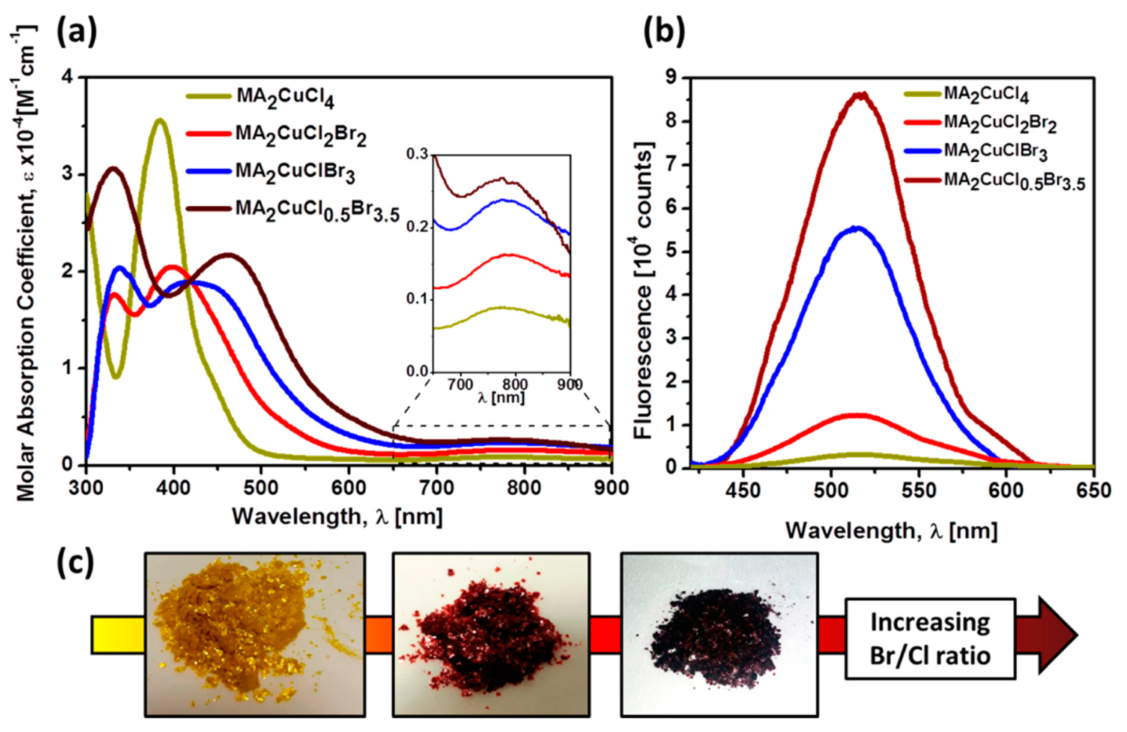
4.1. Cu-Based 2D Perovskite Absorbers

Cortechia and coworkers were the first to demonstrate and report the possible use of 2D copper perovskite through absorbers and provided a background intended for more studies on the development of transition metal-based perovskites as lead-free replacement materials. A sequence of (CH3NH3)2CuClxBr4−x, based on a starting material of an aliphatic amine, was studied, whereby the role of the Br/Cl ratio was found to be responsible for material stability and optical characteristics. The exploitation of added Cu d–d charge transfer and fittingly tailoring the proportion of Br/Cl, which likewise influences ligand-to-metal charge transfer transitions, extended the optical absorption in the sequence of the compound to near-infrared for optimum spectra-overlaying irradiance. In the sequence of (CH3NH3)2CuClxBr4−x, it was observed that their correlated values of 2.48 eV (500 nm) for MA2CuCl4 and 1.8 eV (689 nm) for MA2CuCl0.5Br3.5 optical bandgaps could be tailored by accruing the Br substance, whereas a further provision can be implemented for the absorption within the range of 700 and 900 nm on or after transitions within d Cu levels as shown in Figure 10. Besides, the charge transfers and d−d transitions were displayed in the direction that strongly results in photocurrent production. Using MA2CuCl2Br2 as a sensitizer of the series, a value of 0.0017% was obtained for power conversion efficiency [123].
Similarly, Elseman et al. reported a series of Copper-centered mixed perovskite materials, with the common formulation of (CH3NH3)2CuX (X = Cl4, Cl2I2, and Cl2Br2) for perovskite solar cells. The chlorine ion (Cl) in the structure was found to be responsible for the stabilization of the formed compound. The obtained results showed that (CH3NH3)2CuCl4 produced an optical bandgap of 2.36 eV and a power conversion efficiency of 2.41%, whereas they were 0.99 eV and 1.75% for (CH3NH3)2CuCl2I2 and 1.04 eV and 0.99% for (CH3NH3)2CuCl2Br2. It was observed that (CH3NH3)2CuCl2Br2 provided a far lesser conversion efficiency despite its optimized bandgap. The lower performance of (CH3NH3)2CuCl2Br2 can be explained due to Cu2+ reduction caused by the higher trap density. Green photoluminescence of the perovskite materials was achieved due to Cu+ ions [125]. However, Li and coworkers reported an aromatic amine of the 2D-layered (C6H5CH2NH3)2CuBr4 perovskite. The compound exhibited a bandgap value of 1.81 eV, whereby at an intense absorption of 539 nm, it gave rise to a high absorption coefficient with a value of around ∼1 × 105 cm−1, thereby inferring its suitability for photon harvesting in thin-film solar cells. The analytical results of XRD, UV–vis absorption, and TGA confirmed the compound’s significant stableness when exposed to humidity, heat, and ultraviolet light. By perovskite exploitation in mesoscopic solar cells, a 0.2% conversion efficiency was obtained [126].
Meanwhile, Hajiaoui and co-workers synthesized a copper-based hybrid perovskite using chlorine substituted in an aliphatic amine as a starting precursor. A novel layered 2D perovskite material of [Cl(CH2)2-NH3]2[CuCl4] was developed, wherein 2-chloroethylammonium positively charged ions fills the voids surrounding the CuCl6 octahedra. The structural analysis indicates that the phase transition in the area of T1 = 281 K is induced by an unusual boat-to-chair conformation change of some of the 2-chloroethylammonium cations and the reorientation displacement of [CuCl6]n4− zigzag chains. The perovskite material exhibited an indirect bandgap equal to 1.98 eV. The small activation energy (0.26 eV) at low temperature indicates that conduction, with the measurement between 10−5 and 10−4 Ω−1 m−1 in the material, can be assured of electronic conduction [127].

4.2. Fe-Based 2D Perovskite Absorbers

By exploring the significant structural diversity on compounds with the common molecular formula A2MX4, whereby A = organic positively charged ions, M = transition metal ions, X = halide negatively charged ions, it is well known that perovskite-related layered structures with octahedral-coordinated M atoms are found, for example, in (CH3NH3)2MCl4 (M = Cu, Mn, Cd, Fe). However, a great number of structures with central M atoms are tetrahedrally coordinated, for example, in (CH3NH3)2MCl4 (M = Zn, Hg) [128]. Even though structures with octahedral-coordinated M atoms are found in (CH3NH3)2FeCl4 in the family of A2MX4, Yin and coworkers were the first to report regular tetrahedron structures found in orthorhombic CH3NH3FeCl4, which is not in the family pattern of A2MX4; thus, they were used to investigate its structure, adsorption properties, and photoelectric behavior. Due to the presence of four Cl ligands coupled with a d5 of Fe3+ and FeCl4−ions, The CH3NH3FeCl4 compound was formed with a bandgap value of almost 2.15 eV. The observed values of the three-emission luminescence were 398, 432, and 664 nm, respectively. The solar device built on the assembly of the FTO/TiO2/MAFeCl4/carbon electrode attained photoelectric conversion efficiency of 0.054% with a value of 0.319 V voltage source, a photocurrent of 0.375 mA cm−2, and a 0.45 fill factor under an AM1.5, 100 mW cm−2 simulated illumination [124].

4.3. Pd-Based 2D Perovskite Absorbers

Even though the magnitude bounds projected through the Goldschmidt tolerance factor formula were higher than the magnitude of the organic cation of Pd-based 2D perovskites, Huang and co-workers showed the preparation of a previously unknown (CH3NH3)2PdCl4 compound. The prepared material has a compounds phase bulk resistivity value of 1.4 Ωcm−1, a direct bandgap of 2.22 eV, and an absorption coefficient of 104 cm−1. The XRD analysis of (CH3NH3)2PdCl4 showed to be moderately stable in the air when compared to numerous present in hybrid perovskites that are disposed to phase deterioration when open to ambient air [18]. Furthermore, Zhou et al. synthesized a series of organic–inorganic layered Pd-centered perovskites, such as (CH3NH3)2PdCl4, (CH3NH3)2PdCl4−xBrx, and (CH3NH3)2Pdl3 and studied the adsorption properties and photoelectric behavior. The (CH3NH3)2PdCl4 compound exhibited an absorption band of 600 nm with a bandgap value of 2.15 eV, while (CH3NH3)2PdCl4−xBrx, displayed a band of 700 nm with a bandgap of 1.87 eV, as well as a band of 1000 nm coupled with a bandgap value of 1.25 eV for (CH3NH3)2PdCl4−xBrx. Interestingly, the photoelectric response of CH3NH3PdI3 reached 950 nm. The results have drawn attention in the fields of optoelectronics and photovoltaics [129].

4.4. Mn-Based 2D Perovskite Absorbers

By exploiting the impressive luminescent and photoelectric properties, 2D layered Pb-free hybrid perovskites have exhibited practical applications in optoelectronic and photovoltaic devices [130]. Nie et al. reported the photoresponse of (CH3NH3)2MnCl4 in a photoelectric device. The solution-processed (CH3NH3)2MnCl4 thin layer displayed its position alongside the b-axis route on the TiO2 area. The photoelectric cell through the FTO/TiO2/(CH3NH3)2MnCl4/ carbon electrode showed evident photoresponses detected beneath 10−30 Hz flashlight frequencies and a 330 nm light beam. This modest photoresponsive device may be impactful in the future for industrialized assembly of photosensitive recorders and memory devices [130].
Furthermore, Cheng et al. reported centimeter-size square 2D-coated single crystals of (CH3NH3)2MnCl4 perovskite. The single crystals of (CH3NH3)2MnCl4 were developed by a varied crystal network (squares and octagon) using different organic solvents and concentrations of hydrochloric acid solution. Comparing the powder XRD analysis of both (CH3NH3)2MnCl4 single crystals, the results showed that they equally fit into the equivalent crystal coordination and have equivalent cell factors. Photons can sensitize these materials in diverse wavelength bands. The key band remains situated at 608 bases on its emission spectra and is placed at 72 nm full width at half maximum (FWHM) through an excellent elongated lifetime of microseconds.
Moreover, LED appliances’ optoelectronic application was organized based on the (CH3NH3)2MnCl4 single crystals, with LED being prepared for the single crystals of (CH3NH3)2MnCl4. The results showed that the single crystal of (CH3NH3)2MnCl4 has suitable luminescence effects, can radiate evident red light, and be applied for white light illumination. Hence, the unique luminescence properties of the (CH3NH3)2MnCl4 single crystal equally show that it can be used for the application of perovskite solar cells [24].

5. Perovskite-Like Halide Absorbers (A3B2X9)

The compound halides of bismuth and antimony all possessing a valence of three are known to not have the ability to adapt the same perovskite structures of three-dimensional (3D) perovskite frameworks with common formula of ABX3. These compositions are inclined to develop zero-dimensional, one-dimensional, and two-dimensional (2D) perovskite-like halide absorbers with properties featuring varying sizes agreeing to the direction of measurement due to the purpose of quantitative relations between the reactants [27]. These perovskite-like halide absorbers are a structurally rich group of mixed organic−inorganic halide perovskites from the extensive family of A3B2X9 structures, where A represents monovalent positively charge ions = Cs+, Rb+, or CH3NH3+ alias MA+; B stands for the positively charged trivalent metal ions = Bi3+, Sb3+; and X denotes negatively charged ions of halides = (Cl, Br, or I) employed as active photovoltaic absorbers [45,131,132,133].
In the group of A3B2X9 compositions, the A and X atoms are situated in the orientation of closest packing, and B atoms tend to fill two-thirds of the octahedral X6 voids. The two main types of A3B2X9 compounds are the 0-D dimer phase of hexagonal close packing and the 2-D layered phase of cubic tight packing of A and X atoms [134], as shown in Figure 11. When small cations (Cs or Rb) are used, the two-dimensional (2D) layered perovskite-like structures are formed. Meanwhile, the zero-dimensional (0D) dimers are produced when large cations (e.g., MA) are used. The Sb- and Bi-based perovskites are the two kinds of materials that are more stable in air and moisture than Pb-based perovskites [135]. Herein, a summary of device performance on selected lead-free perovskite-like solar cells is displayed in Table 6.

5.1. Sb-Based Perovskite-Like Halides

Antimony is a group 15 element, and existing in its stable + 3 states can form either a 2-D layered perovskite structure or a 0-D dimer [135]. Generally, when a trivalent metal positively charged ion of Sb3+ replaces a bivalent heavy metal positively charged ion of (Pb2+) in ABX3 perovskite, it results in the transformation of a defect-order structure of A3B2X9 perovskite [136]. These antimony-based perovskite-like halide materials belong to the family of A3B2X9 perovskites. Saparov and coworkers were the first to report the 2D composition of the layered pattern of Cs3Sb2I9 that has a bandgap value of 2.05 eV, whereby this experimental value is in alignment with the calculated theoretical value of 2.06 eV [146]. Furthermore, Singh et al. reported the inorganic layered Sb-based perovskite Cs3Sb2I9 using solution processing to obtain an optical bandgap value of 2.05 eV. A solar cell device with an assembly of inorganic layered Cs3Sb2I9 perovskite (ITO/PEDOT (PSS poly(3,4-ethylenedioxythiophene) poly(styrenesulfonate)): PSS/Cs3Sb2I9/PC71BM/Al) displayed a value of 0.72V for its voltage source, a photocurrent of 5.31 mA cm−2, and a value of 0.39 for its fill factor, thereby reaching power conversion efficiency of 1.49% under AM1.5G solar illumination. Using the principal device to integrate the dimer model displayed a voltage source value of 0.77 V, a photocurrent of 2.82 mA cm−2, and a fill factor of 0.40, thereby reaching a PCE of 0.89% [137].
Through the solvent engineering method with a toluene drop throughout the spin-coating procedure, Hebig et al. introduced the methylammonium antimony iodide (CH3NH3)3Sb2I9 0D perovskite as a promising material with the aim of producing lead-free solar devices. The unstructured layers of (CH3NH3)3Sb2I9 were determined to have a peak absorption coefficient of around α ≈ 105 cm−1 and optical bandgap of 2.14 eV. A planar heterojunction device was fabricated to ascertain the potential of (CH3NH3)3Sb2I9 as a light harvester for photovoltaic applications, which yielded around η ≈ 0.5% conversion efficiency, previously presenting a defined fill factor of 55% and a voltage source of 0.89 V, but low photocurrent densities. Through enhancing the contact layers and the morphology of the Sb-perovskite, far greater power conversion efficiencies may be achievable [138].
Recently, Karuppuswamy et al. (2018) employed antisolvent conduct to the surface morphology enhancement of the Sb-centered dimer of (CH3NH3)3Sb2I9 crystals by speeding up heterogeneous nucleation. This process was achieved by incorporating an interlayer that performed as favorable hydrophobic support for the growth of large-grain (CH3NH3)3Sb2I9 crystals, thereby reducing the number of spaces and growing the film property. A bandgap of 1.9 eV was obtained. By incorporating the Sb-based perovskite-like photoabsorbers as the active layer on fabricated inverted planar heterojunction PSCs, the photovoltaic properties displayed a voltage source value of 0.77 V resulting from a photocurrent of 6.64 mA cm−2 and a fill factor of 59.60%, thereby reaching a PCE of 2.77% [135].
By replacing the A cation of either Cs or CH3NH3 with Rb cation, Harikesh and co-workers demonstrated the solution-processed Sb-based perovskite of Rb3Sb2I9, which obtained values of 2.24 and 2.1 eV of direct and indirect bandgaps. The fabricated solar device exhibited a voltage source of 0.55 V and a photocurrent of 2.12 mA/cm2 short circuit current density, and it achieved efficiencies of up to 0.66% [139]. Recently, Correa-Baena et al. reported Sb-based compounds of 2D layered Rb3Sb2I9 which achieved a 2.03 eV direct bandgap and yielded a 0.76% power conversion efficiency, including features such as a voltage source of 0.66 V, a photocurrent of 1.84 mA cm−2 and a fill factor value of 0.63 [147]. Furthermore, Weber et al. investigated the control of changing the bromide proportion to the iodide proportion on the structural, optical, and photovoltaic properties of Rb3Sb2Br9−x Ix (x = 0–9). Sequential replacement of iodide with the lesser bromide does not alter the crystal coordination; however, compounding the bromide substance ends in a reduction of the unit cell, in addition to in a blue shift of the absorption onset, raising the bandgap from 2.02 to 2.46 eV. The fabricated unveiled solar cells with Rb3Sb2I9 (Px = 0–9), as the light harvester exhibited photovoltaic properties presenting values of Voc = 0.55 V, Jsc = 4.25 mA cm−2, and fill factor = 59.5%, reaching a PCE of 1.37% [140].
Based on replacing the A cations of either Cs or CH3NH3 with NH4 and adjusting the halide, Zuo et al. prepared an (NH4)3Sb2IxBr9−x (0 ≤ X≤ 9) group of perovskite absorbers by using an anti-solvent vapor-assisted crystallization method. The light-harvesting of the (NH4)3Sb2IxBr9−x perovskite material was tailored by modifying I and Br content. The family members such as (NH4)3Sb2I9, (NH4)3Sb2I6Br3, (NH4)3Sb2I3Br6, and (NH4)3Sb2Br9 layers show direct optical bandgaps of 2.27 eV,2.49 eV, 2.66 eV and 2.78 eV, respectively. The atomic force microscope (AFM) analyzed the (NH4)3Sb2I9 layer, and the result showed that the layer had somewhat compact and uniform morphology. Upon using the formation of ITO/PEDOT:PSS/(NH4)3Sb2I9/PC61BM/Al in solar cells, the performing photovoltaic characteristics of (NH4)3Sb2I9 by way of the end member were investigated to give a Voc of 1.03 V, a Jsc of 1.15 mAcm−2, a fill factor of 42.88%, and a PCE of 0.51%. The Voc of the (NH4)3Sb2I9 perovskite solar cell is known to be much higher than the Voc of most lead-free perovskite solar cells. Hence, the improvement of (NH4)3Sb2I9 perovskite crystallinity will increase hole and electron mobilities and enhance the power conversion efficiency [141].
Comparing the performance of Sb-based perovskite-like halides, Boopathi and co-workers demonstrated a single-step technique to formulate solution-processable (CH3NH3)3Sb2I9 and Cs3Sb2I9 perovskite thin films. The use of precursor molar ratios and HI additive concentrations produced stoichiometric perovskite films, whose crystalline phases were analyzed through XRD. The new HI addictive technique gave rise to greatly improved perovskite thin film. SEM images of processable (CH3NH3)3Sb2I9 and Cs3Sb2I9 perovskite materials exhibited different morphologies due to their differences in light absorption and device performance. The optical bandgaps of (CH3NH3)3Sb2I9 and Cs3Sb2I9 were evaluated as 1.95 and 2.0 eV and were influenced by their respective morphologies, as shown in Figure 12. Using (CH3NH3)3Sb2I9 perovskite material in an assembly of planar device architecture solar cells, a PCE of 2.04% was obtained. However, for the assembly of the solar devices with CH3NH3)3Sb2I9 perovskite material, a PCE of 0.5% was previously obtained by Hebig and co-workers as well as Zuo and co-workers, which remained lower than the present value of 2.04%. This is in the right step towards achieving perovskite-like halides to serve as materials for photovoltaic application. The photovoltaic performance parameters of champion Sb-based perovskite devices fabricated with and without the HI additive such as with bare MA3Sb2I9 yielded a PCE of 1.11% and a voltage source of 0.6 V; MA3Sb2I9 + HI obtained a 2.04% PCE and a VOC of 0.62 V; bare Cs3Sb2I9 attained a 0.67% PCE and a voltage source of 0.62 V; and Cs3Sb2I9 + HI yielded a PCE of 0.84% and a voltage source of 0.60 V [142].
To resolve the subject of the wide optical bandgap linked by the (CH3NH3)3Sb2I9 perovskite compound, Chatterjee and Pal introduced Sn4+ at the metallic position of the antimony-based defect-ordered mixed iodide (CH3NH3)3Sb2I9 perovskite structure, resulting in a steady shift in the electronic transfer by the perovskites with an optical gap value of 2 eV which was successfully lowered to around 1.55 eV. Using the scanning tunneling spectrometry and density-of-state spectra analysis, a remarkable shift of Fermi energy in the direction of the conduction band edge occurred due to a rise in the Sn substance held within the perovskite. This shift brought about in tailoring a kind of electronic potential from the p-type to the n-type and, essentially, led to a better bandgap configuration with the selective connections of p–i–n heterojunctions. Nevertheless, the surface coarseness of the perovskite layer was adversely affected due to tin inclusion. Therefore, the tin substance was enhanced by taking prevailing factors, namely, the bandgap of the compound and the surface coarseness of thin layers, into account. The fabricate heterojunction device with 40% tin as a substitute for antimony enshrined in (CH3NH3)3(Sb1−x Snx)2I9 perovskite exhibited the following photovoltaic properties: a voltage source value of 0.56 V, a photocurrent of 8.32 mA cm−2 and a fill factor of 58%, reaching a PCE of 2.69% [136].
Moreover, in a bid to resolve the issue of deprived layer morphology and overwhelming halide components associated with the (CH3NH3)3Sb2I9 perovskite material, which are results of the disorder of growth progression, Yang et al. introduced bis(trifluoromethane)sulfonimide lithium (LiTFSI) into (CH3NH3)3Sb2I9 perovskite material to produce high-level property two-dimensional (CH3NH3)3Sb2I9−xClx layers. Through the linker molecule surrounded by Sb-based pyramidal groups, LiTFSI is responsible for providing a zero-dimensional in-between state and impeding crystallization. The gradual conversion of dimensions will steady the bandgap of perovskite-like layers with a constant Cl/I ratio (∼7:2), preventing the arbitrary “x” quantity in (CH3NH3)3Sb2I9−xClx layers made from the traditional technique. By using this technique, Sb-based perovskite-like solar cells (PLSCs) obtained a maximum power conversion efficiency (PCE) of 3.34% and retained 90% of the preliminary PCE when kept under ambient surroundings for about 1400 h [143].

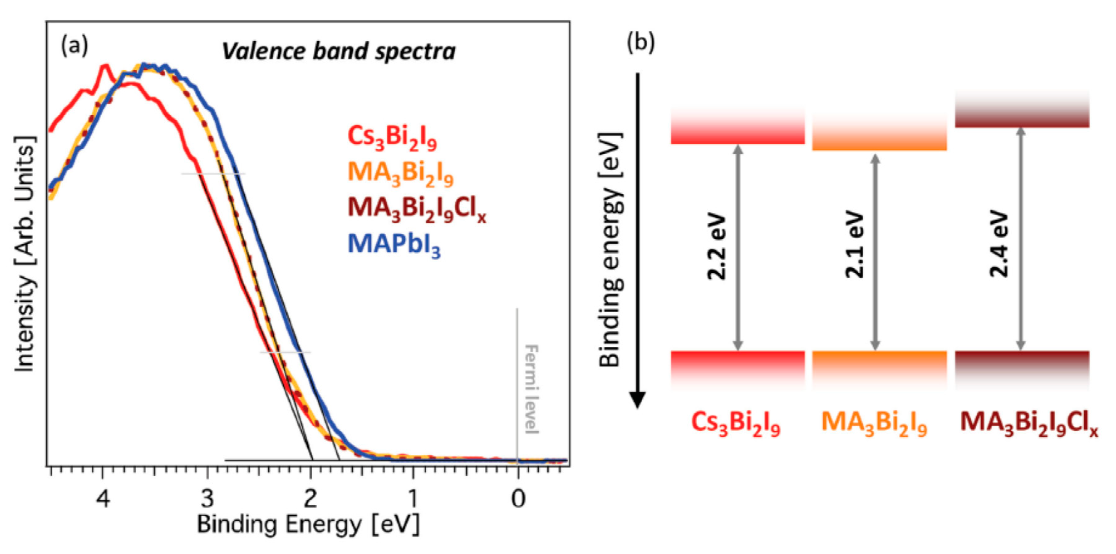
5.2. Bi-Based Perovskite-Like Halides

Bismuth belongs to a group of 15 elements and is the only one among the 6p block elements with an outer lone pair of 6s2 electrons of lead [148]. Due to the Bi3+ outer lone pair of 6s2 electrons, the equal numbers of electrons or equivalent electronic structure, and the way by which its electron cloud is deformed by electric fields, as seen in Pb2+, bismuth-based perovskite-like halide crystal chemistry is related to the lead halide perovskite such that the rich structural diversity of the Bi-based compound is detected containing deformation, space sites, and numerous methods for the combination of the MX6 octahedra. However, Bi3+ has a propensity to form compositions of subordinate dimensionality when compared to the metal halide groups of Pb2+ [134]. The formed structures of lower dimensionality vary from systems based on isolated (0D) inorganic polyhedral to one-dimensional (1D) ones with extended chains, right up to two dimensional (2D) networks [149]. The first crystal structure of bismuth perovskite of Cs3Bi2I9 was studied in the 1960s. After a period of 50 years, Park and co-workers were the first to incorporate bismuth perovskite of Cs3Bi2I9 into solar cells [150]. Using a one-step spin coating method, Park et al. prepared the perovskite materials of Cs3Bi2I9, MA3Bi2I9, and MA3Bi2I9−xClx. XRD analysis showed that all samples were of a hexagonal crystalline phase and in the space group P63/mm. The three materials, MA3Bi2I9, MA3Bi2I9Clx, and Cs3Bi2I9, were analyzed through an X-ray photoelectron spectroscopy, whereby the estimated I/Bi ratios, such as 4:4, 4:7, and 4:6, were used for their formation. Hence, the investigation gives rise to the valance band spectra and energy level diagram shown in Figure 13. The bandgaps were approximated to be around 2.1, 2.2, and 2.4 eV for the MA3Bi2I9, Cs3Bi2I9, and MA3Bi2I9−xClx samples. Among the perovskites, Cs3Bi2I9 recorded the best photovoltaic parameters, which were determined as a photocurrent of 2.15 mAcm−2, a voltage source of 0.85 V, and a fill factor value of 0.60, and they attained a PCE of 1.09%. Hence, the recorded power conversion of the Cs3Bi2I9 perovskite material was greater than the two other perovskites: a PCE of η = 0.12% for MA3Bi2I9 and η = 0.003% for MA3Bi2I9−xClx [151].
Recently, Ma and co-workers also reported also the synthesis of millimeter-scale single crystals of Cs3Bi2I9 and MA3Bi2I9 perovskites via a facile hydrothermal approach. The Cs3Bi2I9 and MA3Bi2I9 single crystals exhibited similar light absorption properties, both holding an approximated bandgap of 1.9 eV. Spin-coating of these compounds produced thin films with uniform surface morphologies, superior carrier mobility, and more stability. By assembling a solar cell (utilizing a spin-coating procedure), the optoelectronic properties of these compounds were tested. The solar device with the MA3Bi2I9 compound obtained a 0.2% PCE with the following parameters: a voltage source of 0.53 V, a photocurrent of 0.65 mA cm−2, and a fill factor value of 0.57. Similarly, the Cs3Bi2I9 perovskite solar cell obtained a PCE of 0.18%, which was achieved with Jsc = 0.58 mA cm−2, Voc = 0.54 V, and FF = 57%. The power conversion efficiencies obtained in these studies were higher than the PCEs reported by Park et al. (2015). These findings indicate that the electrical properties of these compounds could further be optimized to enhance the performance of photoelectric devices [152].
By XRD analysis, CsBi3I10 thin film has a layered composition with varying control of crystal development when compared to the Cs3Bi2I9 perovskite. A bandgap value of 1.77 eV was achieved for of CsBi3I10 film, while a bandgap value of 2.03 eV was achieved for of Cs3Bi2I9 perovskite.
Johansson and coworkers reported the photo-conversion of non-toxic bismuth materials, such as Cs3Bi2I9 and CsBi3I10, and a comparison of their morphologies was made by Park et al. in 2015 with a focus on Cs3Bi2I9 perovskite material [153]. By XRD analysis, CsBi3I10 thin film has a layered composition with varying control of crystal development when compared to Cs3Bi2I9 perovskite. A bandgap value of 1.77 eV was achieved for CsBi3I10 film, while a bandgap value of 2.03 eV was achieved for Cs3Bi2I9 perovskite. The light absorption of CsBi3I10 showed a band of up to 700 nm, while Cs3Bi2I9 perovskite showed a band of up to 600 nm. The improved light absorption based on CsBi3I10 when compared to that of Cs3Bi2I9 perovskites was attributed to its surface morphology having uniform coverage [153]. Recently, Ghosh et al. 2018 critically assessed Cs3Bi2I9 to have an approximated bandgap of 2 eV and noted it as a composition designed for a thin layer light harvester with a conversion efficiency that was described as firmly deficient due to the low photocurrent density. Therefore, Ghosh et al. 2018 suggested that by varying the stoichiometry of the starting materials, the power conversion efficiency of the Cs3Bi2I9 solar cell would be somewhat enhanced [154].
To corroborate and improve on the work of Park et al. in regard to the MA3Bi2I9 perovskite compound, other scientists reported the synthesis of the MA3Bi2I9 perovskite compound featuring different photovoltaic properties. Oz et al. reported that the MA3Bi2I9 perovskite compound exhibited a wide bandgap value of 2.9 eV, and, upon optical excitation, photoluminescence emission was recorded at 1.65 eV (751 nm). The PCE was close to 0.1% upon the fabrication of MA3Bi2I9 layers in a solar cell with a planar heterojunction configuration (ITO/PEDOT/ (CH3NH3)3Bi2I9/PCBM/Ca/Al) [155]. Singh et al. reported the slightly improved photovoltaic performance with 0.2% PCE through an appropriate cell configuration of MA3Bi2I9 composition using planar, brookite, and anatase mesoporous layers for a structured photovoltaic perovskite [131]. Zhang et al. reported the enhanced efficiency of MA3Bi2I9-based solar cells, reaching 0.42% with mesoscopic architecture on a TiO2/ITO substrate through a one-step spin-coating. Relatively high values were exhibited: Voc = 0.66 V and fill factor = 62.48% [156].
Furthermore, Ran et al. reported a plane, constant, and dense MA3Bi2I9 thin film being produced through a new two-step evaporation–spin-coating layer invention approach [157]. Using an inverted planar heterojunction photovoltaic device, the MA3Bi2I9 thin film exhibited a value of Voc = 0.83 V, reaching a PCE of 0.39% [157]. Zhang et al. reported the adoption of a two-stage technique—high-vacuum BiI3 discharge and low-vacuum uniform MA3Bi2I9 conversion—to harvest dense, pinhole-free, and fine-crystallized MA3Bi2I9 layers with large submicron-micron granules. Due to the ideal morphologies of MA3Bi2I9 when compared to previously synthesized MA3Bi2I9 perovskites, the target MA3Bi2I9 films in the solar cell device exhibited a 1.64% PCE with all three J-V parameters displaying a voltage source value of 0.83 V, a short circuit current of 3.00 mA cm−2, and a fill factor value of = 0.79, overcoming or, in the same way, reaching the best values to date for MA3Bi2I9 solar cells [144]. However, Jain et al. reported the enhancement in crystallinity and surface morphology of methylammonium bismuth iodide (MAI), whereby through a controlled, stepwise formation of methylammonium bismuth iodide (CH3NH3)3Bi2I9 perovskite films synthesized via the vapor-assisted solution process (VASP) by exposing BiI3 films to CH3NH3I (MAI) vapors for several reaction times, (CH3NH3)3Bi2I9 semiconductor layers with tailoring optoelectronic characteristics were attained. With good reproducibility, solar cells prepared on mesoporous TiO2 substrates obtained hysteresis-free efficiencies of up to 3.17%. This good performance is attributed mainly to the uniform surface coverage, enhanced stoichiometry, lowered metallic substance in the bulk, and the anticipated optoelectronic attributes of the absorbers [158].
Through A-site cation substitutions of either Cs or CH3NH3/MA with NH4 cation, Sun et al. reported the synthesis of (NH4)3Bi2I9 perovskite, which was made from the solution and composition elucidated by single-crystal X-ray diffraction. An approximated bandgap of 2.04 eV was obtained and, thus, was considered to be lower than that of CH3NH3PbBr3 at 2.20 eV [159]. Recently, Lan et al. in 2019 reported that the A-site cation substitutions in lead–halide perovskites altered their optical properties, and they therefore prepared a novel formamidinium (FA)-based bismuth perovskite material, (FA)3Bi2I9. (FA)3Bi2I9 showed a hexagonal phase with a more distended unit cell when compared with the traditional methylamine-based bismuth perovskite (MA)3Bi2I9. The perovskite compound exhibited a bandgap of 2.19 eV. The mesoporous-coordinated (FA)3Bi2I9 solar cells were assembled and showed a value of Voc = 0.48 V, reaching a PCE of 0.022%. Thus, they were considered to be a development allowing researchers to move beyond the methylamine-based bismuth perovskite solar cells, proposing a possible light harvester for lead-free perovskite solar cells [145]. Furthermore, Li et al. reported the synthesis of three novel organic–inorganic iodobismuthate containing organic positively charged ions with heterocyclic 5-membered rings by way of various inorganic structures beginning with 0D for [TH]3[Bi2I9] and [IM]3[Bi2I9], as well as ending with 1D [AT][BiI4] (TH = thiazolium, IM = imidazolium and AT = amino thiazolium). The direct optical bandgap values were redshifted from 2.08 eV for [TH]3[Bi2I9] and 2.00 eV for [IM]3[Bi2I9] to 1.78 eV for [AT][BiI4], determined by UV–vis reflectance spectroscopy. For electron injection purposes and to enable an enhanced energy level to match TiO2, the conduction band minimum (CBM) value of [AT][BiI4] was shifted to a lower value. Though the main influences of Bi 6p and I 5p antibonding associations were found for [AT][BiI4], theoretical studies showed that additional contribution of organic entities in the conduction band minimum could be found for [TH]3[Bi2I9]. By using [AT][BiI4] as the light absorber in a hole-conductor-free, completely printable solar cell with relatively good reproducibility, a power conversion efficiency of 0.47% was obtained [160].

6. Conclusions and Prospects

This review focused on the current understanding as to the substitution of lead via both homo- and hetero-valent substitution and its influence on various halide perovskite materials as well as their photovoltaic properties. Furthermore, the collective outcomes from the experimental findings on the hybrid lead-free halide metal perovskite were discussed with emphasis on how chemical compositions influence optical and morphological properties, and the limitations to aid future studies were identified.
Perovskite solar cells have inherently faced the drawback of upscaling the technology to the commercialization of energy and wide deployment of its outdoor applications due to the presence of harmful chemicals such as lead(II) halide materials in lead-based perovskites. The utilization of lead(II) halide materials in perovskite solar cells has raised environmental concerns, and a considerable number of questions has drawn attention to the feasibility of using solar cells technology that incorporates soluble lead(II) compounds due to toxicity, as well as the potential threat that the widespread deployment of the technology could pose on the environment. Moreover, these perovskite materials have questionable long-term stability. Hence, the metal substitution of lead in the perovskite composition can be essential by way of compositional fixing to tailor its optical, morphological, and electronic properties.
The structural dimensionality and the type of B cation to substitute for Pb are the two important factors that will determine the suitability of halide perovskite material for photovoltaic applications. This structural dimensionality and the type of B cations were reported in the following order of dimensions: 3D single perovskites, double perovskites, two-dimensional (2D), and perovskite-like halides with the common formula of A3B2X9. For the 3D perovskite, we observed the incomplete replacement of monovalent methylammonium (MA) positively charged ions by hydrazinium (HA) ions to enhance the stableness of MASnI3 films and improve their morphology, thereby giving rise to remarkable enhancement in the PCE of the solar cells. As regards the B positively charged ions, the replacement of Pb by Ge, Sn, Cu, Fe, Pd, Mn, Sb, or Bi obtained lower PCE values when compared to those described with MAPbI3.
The B cation is primarily the cation that governs the kind of perovskite crystal formation as well as the photovoltaic characteristics of the perovskite materials due to the specific electronic composition of each B cation. Moreover, for every given perovskite structure with the general formula of ABX3, their different chemical compositions of all the perovskite materials strongly determined their bandgaps. This is because the chemical composition made of different elements has different orbital energies and characters. The A cation is highly ionic and makes little contribution to the band edges. Therefore, the optical bandgap is mainly governed by the B cation and the X anion, which form the [BX6] octahedra framework. Furthermore, the optimization of the morphology is realized through mixed compositions. In some cases, morphology optimization is influenced through the concentrations of the perovskite precursors in the solution and the speed rotation.
Since the composition of the perovskite crystals directly controls the photovoltaic properties of the perovskite solar cells, the recommendation, therefore, is for systematic structural variations of unique components to be continuously carried out under the required reaction conditions in order to optimize their morphology properties via additives that suppress recombination due to the need for the exact amounts of components for hybrid perovskite.

Author Contributions

S.J.A. conceived the outlines and contents and wrote the review; E.L.M.—funding acquisition. All authors have read and agreed to the published version of the manuscript.

Funding

This work was based on the research supported in part by the National Research Foundation of South Africa (NRF), grant number (GUN: 120763). We thank the Department of Science and Innovation (DSI), Eskom Tertiary Education Support (TESP), and Govan Mbeki Research and Development Centre (GMRDC) for supporting this research.

Acknowledgments

The authors thank the National Research Foundation of South Africa (NRF) Department of Science and Innovation (DSI), Eskom Tertiary Education Support (TESP), and Govan Mbeki Research and Development Centre (GMRDC) for financial assistance.

Conflicts of Interest

The authors declare no conflict of interest

Abbreviations

0-Dzero-dimensional
1-Done-dimensional
2-Dtwo-dimensional
3-Dthree-dimensional
EgBandgap
FAFormamidinium
FFfill factor
FTOfluorine-doped tin oxide
ITOindium tin oxide
JscShort-circuit current
(LiTFSI)bis(trifluoromethane)sulfonimide lithium
MAmethylammonium
PC71BM[6,6]-phenyl C71butyric acid methyl-ester
PCBM[6,6]-phenyl-C61-butyric acid methyl ester
PC61BM[6,6]-phenyl-C61-butyric acid methyl ester
PCEpower conversion efficiency
PEDOT: PSSpoly(3,4-ethylenedioxythiophene) poly(styrenesulfonate)
PSCsperovskite solar cells
PLPhotoluminescence
PVPhotovoltaics
SEMScanning electron microscope
spiro-OMeTAD2,20,7,70-tetrakis-(N,N-di-p-methoxyphenylamine)9,90-spirobifluorene
TGA Thermogravimetric analysis
Vocopen circuit voltage
XRDX-ray diffraction
UV-visultraviolet-visible absorption

References

  1. Mutalikdesai, A.; Ramasesha, S.K. Emerging solar technologies: Perovskite solar cell. Resonance 2017, 22, 1061–1083. [Google Scholar] [CrossRef]
  2. Heo, J.H.; Han, H.J.; Kim, D.; Ahn, T.K.; Im, S.H. Hysteresis-less inverted CH 3 NH 3 PbI 3 planar perovskite hybrid solar cells with 18.1% power conversion efficiency. Energy Environ. Sci. 2015, 8, 1602–1608. [Google Scholar] [CrossRef]
  3. Snaith, H.J.; Abate, A.; Ball, J.M.; Eperon, G.E.; Leijtens, T.; Noel, N.K.; Stranks, S.D.; Wang, J.T.-W.; Wojciechowski, K.; Zhang, W. Anomalous hysteresis in perovskite solar cells. J. Phys. Chem. Lett. 2014, 5, 1511–1515. [Google Scholar] [CrossRef] [PubMed]
  4. Park, N.-G. Perovskite solar cells: An emerging photovoltaic technology. Mater. Today 2015, 18, 65–72. [Google Scholar] [CrossRef]
  5. NREL Solar Cell Efficiency Chart. Available online: https://www.nrel.gov/pv/cell-efficiency.html (accessed on 17 September 2020).
  6. Wang, L.; Wang, K.; Zou, B. Pressure-induced structural and optical properties of organometal halide perovskite-based formamidinium lead bromide. J. Phys. Chem. Lett. 2016, 7, 2556–2562. [Google Scholar] [CrossRef] [PubMed]
  7. Saliba, M.; Matsui, T.; Seo, J.-Y.; Domanski, K.; Correa-Baena, J.-P.; Nazeeruddin, M.K.; Zakeeruddin, S.M.; Tress, W.; Abate, A.; Hagfeldt, A. Cesium-containing triple cation perovskite solar cells: Improved stability, reproducibility and high efficiency. Energy Environ. Sci. 2016, 9, 1989–1997. [Google Scholar] [CrossRef] [Green Version]
  8. Wang, F.; Bai, S.; Tress, W.; Hagfeldt, A.; Gao, F. Defects engineering for high-performance perovskite solar cells. npj Flex. Electron. 2018, 2, 1–14. [Google Scholar] [CrossRef] [Green Version]
  9. Chen, Y.; Zhang, L.; Zhang, Y.; Gao, H.; Yan, H. Large-area perovskite solar cells—A review of recent progress and issues. RSC Adv. 2018, 8, 10489–10508. [Google Scholar] [CrossRef] [Green Version]
  10. Gao, P.; Grätzel, M.; Nazeeruddin, M.K. Organohalide lead perovskites for photovoltaic applications. Energy Environ. Sci. 2014, 7, 2448–2463. [Google Scholar] [CrossRef]
  11. Guo, X.; Burda, C. Coordination engineering toward high performance organic–inorganic hybrid perovskites. Coord. Chem. Rev. 2016, 320–321, 53–65. [Google Scholar] [CrossRef]
  12. Loi, M.A.; Hummelen, J.C. Hybrid solar cells: Perovskites under the sun. Nat. Mater. 2013, 12, 1087–1089. [Google Scholar]
  13. Hussain, I.; Tran, H.P.; Jaksik, J.; Moore, J.; Islam, N.; Uddin, M.J. Functional materials, device architecture, and flexibility of perovskite solar cell. Emergent Mater. 2018, 1, 133–154. [Google Scholar] [CrossRef] [Green Version]
  14. Ahmed, M.I.; Habib, A.; Javaid, S.S. Perovskite solar cells: Potentials, challenges, and opportunities. Int. J. Photoenergy 2015, 2015, 1–13. [Google Scholar] [CrossRef] [Green Version]
  15. Tanaka, H.; Oku, T.; Ueoka, N. Structural stabilities of organic–inorganic perovskite crystals. Jpn. J. Appl. Phys. 2018, 57, 08RE12. [Google Scholar] [CrossRef]
  16. Suzuki, A.; Oku, T. Effects of transition metals incorporated into perovskite crystals on the electronic structures and magnetic properties by first-principles calculation. Heliyon 2018, 4, e00755. [Google Scholar] [CrossRef] [PubMed] [Green Version]
  17. Kieslich, G.; Sun, S.; Cheetham, A.K. An extended tolerance factor approach for organic–inorganic perovskites. Chem. Sci. 2015, 6, 3430–3433. [Google Scholar] [CrossRef] [Green Version]
  18. Huang, T.J.; Thiang, Z.X.; Yin, X.; Tang, C.; Qi, G.; Gong, H. (CH3NH3) 2PdCl4: A compound with two-dimensional organic–inorganic layered perovskite structure. Chem. Eur. J. 2016, 22, 2146–2152. [Google Scholar] [CrossRef]
  19. Sun, P.-P.; Li, Q.-S.; Yang, L.-N.; Li, Z.-S. Theoretical insights into a potential lead-free hybrid perovskite: Substituting Pb2+ with Ge2+. Nanoscale 2016, 8, 1503–1512. [Google Scholar] [CrossRef]
  20. Li, Z.; Yang, M.; Park, J.-S.; Wei, S.-H.; Berry, J.J.; Zhu, K. Stabilizing perovskite structures by tuning tolerance factor: Formation of formamidinium and cesium lead iodide solid-state alloys. Chem. Mater. 2016, 28, 284–292. [Google Scholar] [CrossRef]
  21. Travis, W.; Glover, E.N.K.; Bronstein, H.; Scanlon, D.O.; Palgrave, R.G. On the application of the tolerance factor to inorganic and hybrid halide perovskites: A revised system. Chem. Sci. 2016, 7, 4548–4556. [Google Scholar] [CrossRef] [Green Version]
  22. Maughan, A.E.; Ganose, A.M.; Almaker, M.A.; Scanlon, D.O.; Neilson, J.R. Tolerance factor and cooperative tilting effects in vacancy-ordered double perovskite halides. Chem. Mater. 2018, 30, 3909–3919. [Google Scholar] [CrossRef]
  23. Bartel, C.J.; Sutton, C.; Goldsmith, B.R.; Ouyang, R.; Musgrave, C.B.; Ghiringhelli, L.M.; Scheffler, M. New tolerance factor to predict the stability of perovskite oxides and halides. Sci. Adv. 2019, 5, eaav0693. [Google Scholar] [CrossRef] [PubMed] [Green Version]
  24. Cheng, X.; Jing, L.; Yuan, Y.; Du, S.; Yao, Q.; Zhang, J.; Ding, J.; Zhou, T. Centimeter-size square 2D layered Pb-free hybrid perovskite single crystal (CH3NH3)2 MnCl4 for red photoluminescence. CrystEngComm 2019, 21, 4085–4091. [Google Scholar] [CrossRef]
  25. Yi, Z.; Ladi, N.H.; Shai, X.; Li, H.; Shen, Y.; Wang, M. Will organic–inorganic hybrid halide lead perovskites be eliminated from optoelectronic applications? Nanoscale Adv. 2019, 1, 1276–1289. [Google Scholar] [CrossRef] [Green Version]
  26. Kong, D.; Cheng, D.; Wang, X.; Zhang, K.; Wang, H.; Liu, K.; Li, H.; Sheng, X.; Yin, L. Solution processed lead-free cesium titanium halide perovskites and their structural, thermal and optical characteristics. J. Mater. Chem. C 2020, 8, 1591–1597. [Google Scholar] [CrossRef]
  27. Akbulatov, A.F.; Tsarev, S.A.; Elshobaki, M.; Luchkin, S.Y.; Zhidkov, I.S.; Kurmaev, E.Z.; Aldoshin, S.M.; Stevenson, K.J.; Troshin, P.A. Comparative Intrinsic Thermal and Photochemical Stability of Sn (II) Complex Halides as Next-Generation Materials for Lead-Free Perovskite Solar Cells. J. Phys. Chem. C 2019, 123, 26862–26869. [Google Scholar] [CrossRef]
  28. Liu, X.; Yan, K.; Tan, D.; Liang, X.; Zhang, H.; Huang, W. Solvent engineering improves efficiency of lead-free tin-based hybrid perovskite solar cells beyond 9%. ACS Energy Lett. 2018, 3, 2701–2707. [Google Scholar] [CrossRef]
  29. Kim, H.-S.; Hagfeldt, A.; Park, N.-G. Morphological and compositional progress in halide perovskite solar cells. Chem. Commun. 2019, 55, 1192–1200. [Google Scholar] [CrossRef]
  30. Adjokatse, S.; Fang, H.-H.; Loi, M.A. Broadly tunable metal halide perovskites for solid-state light-emission applications. Mater. Today 2017, 20, 413–424. [Google Scholar] [CrossRef]
  31. Li, J.; Cao, H.-L.; Jiao, W.-B.; Wang, Q.; Wei, M.; Cantone, I.; Lü, J.; Abate, A. Biological impact of lead from halide perovskites reveals the risk of introducing a safe threshold. Nat. Commun. 2020, 11, 310. [Google Scholar] [CrossRef] [Green Version]
  32. Urbina, A. The balance between efficiency, stability and environmental impacts in perovskite solar cells: A review. J. Phys. Energy 2020, 2, 022001. [Google Scholar] [CrossRef]
  33. Li, X.; Zhang, F.; He, H.; Berry, J.J.; Zhu, K.; Xu, T. On-device lead sequestration for perovskite solar cells. Nature 2020, 578, 555–558. [Google Scholar] [CrossRef] [PubMed]
  34. Eberstein, M.; Falk-Windisch, H.; Peschel, M.; Schilm, J.; Seuthe, T.; Wenzel, M.; Kretzschmar, C.; Partsch, U. Sintering and contact formation of glass containing silver pastes. Energy Procedia 2012, 27, 522–530. [Google Scholar] [CrossRef]
  35. Sun, X.; Yao, S.; Xing, J.; Zhang, J.; Yang, Y.; Li, H.; Tong, H.; Yuan, X. Mechanism of silver/glass interaction in the metallization of crystalline silicon solar cells. Mater. Res. Express 2020, 7, 016315. [Google Scholar] [CrossRef]
  36. Zhou, J.; Gan, W.; Li, Y.; Huang, B.; Yang, C. Immobilization of silver nanoparticles onto the surface of Pb-based glass frit by a one-pot procedure involving polyol process and its application in conductive thick films. J. Mater. Sci. Mater. Electron. 2015, 26, 234–241. [Google Scholar] [CrossRef]
  37. Zhao, Z.; Gu, F.; Li, Y.; Sun, W.; Ye, S.; Rao, H.; Liu, Z.; Bian, Z.; Huang, C. Mixed-Organic-Cation Tin Iodide for Lead-Free Perovskite Solar Cells with an Efficiency of 8.12%. Adv. Sci. 2017, 4, 1700204. [Google Scholar] [CrossRef] [Green Version]
  38. Chen, Q.; De Marco, N.; Yang, Y.M.; Song, T.-B.; Chen, C.-C.; Zhao, H.; Hong, Z.; Zhou, H.; Yang, Y. Under the spotlight: The organic–inorganic hybrid halide perovskite for optoelectronic applications. Nano Today 2015, 10, 355–396. [Google Scholar] [CrossRef] [Green Version]
  39. Roccanova, R.; Ming, W.; Whiteside, V.R.; McGuire, M.A.; Sellers, I.R.; Du, M.-H.; Saparov, B. Synthesis, crystal and electronic structures, and optical properties of (CH3NH3) 2CdX4 (X = Cl, Br, I). Inorg. Chem. 2017, 56, 13878–13888. [Google Scholar] [CrossRef]
  40. Li, G.; Zou, X.; Cheng, J.; Chen, D.; Yao, Y.; Chang, C.; Yu, X.; Zhou, Z.; Wang, J.; Liu, B. Impact of perovskite composition on film formation quality and photophysical properties for flexible perovskite solar cells. Molecules 2020, 25, 732. [Google Scholar] [CrossRef] [Green Version]
  41. Bin Mohd Yusoff, A.R.; Nazeeruddin, M.K. Organohalide lead perovskites for photovoltaic applications. J. Phys. Chem. Lett. 2016, 7, 851–866. [Google Scholar] [CrossRef]
  42. Reshi, H.A.; Zargar, R.A. Perovskite Solar Cells: The Challenging Issues for Stable Power Conversion Efficiency. Recent Dev. Optoelectron. Devices 2018, 117. [Google Scholar] [CrossRef] [Green Version]
  43. Vidyasagar, C.C.; Muñoz Flores, B.M.; Jiménez Pérez, V.M. Recent Advances in Synthesis and Properties of Hybrid Halide Perovskites for Photovoltaics. Nano-Micro Lett. 2018, 10, 68. [Google Scholar] [CrossRef] [PubMed] [Green Version]
  44. Calvo, M.E. Materials chemistry approaches to the control of the optical features of perovskite solar cells. J. Mater. Chem. A 2017, 5, 20561–20578. [Google Scholar] [CrossRef] [Green Version]
  45. Bhunia, H.; Chatterjee, S.; Pal, A.J. Band Edges of Hybrid Halide Perovskites under the Influence of Mixed-Cation Approach: A Scanning Tunneling Spectroscopic Insight. ACS Appl. Energy Mater. 2018, 1, 4351–4358. [Google Scholar] [CrossRef]
  46. Walsh, A. Principles of chemical bonding and band gap engineering in hybrid organic–inorganic halide perovskites. J. Phys. Chem. C 2015, 119, 5755–5760. [Google Scholar] [CrossRef] [Green Version]
  47. Chen, K.; Schünemann, S.; Song, S.; Tüysüz, H. Structural effects on optoelectronic properties of halide perovskites. Chem. Soc. Rev. 2018, 47, 7045–7077. [Google Scholar] [CrossRef] [Green Version]
  48. Dualeh, A.; Tétreault, N.; Moehl, T.; Gao, P.; Nazeeruddin, M.K.; Grätzel, M. Effect of annealing temperature on film morphology of organic–inorganic hybrid pervoskite solid-state solar cells. Adv. Funct. Mater. 2014, 24, 3250–3258. [Google Scholar] [CrossRef]
  49. Li, W.; Fan, J.; Li, J.; Mai, Y.; Wang, L. Controllable grain morphology of perovskite absorber film by molecular self-assembly toward efficient solar cell exceeding 17%. J. Am. Chem. Soc. 2015, 137, 10399–10405. [Google Scholar] [CrossRef]
  50. Sanders, S.; Stümmler, D.; Pfeiffer, P.; Ackermann, N.; Schimkat, F.; Simkus, G.; Heuken, M.; Baumann, P.K.; Vescan, A.; Kalisch, H. Morphology Control of Organic–Inorganic Bismuth-Based Perovskites for Solar Cell Application. Phys. Status Solidi 2018, 215, 1800409. [Google Scholar] [CrossRef]
  51. Stoumpos, C.C.; Kanatzidis, M.G. Halide Perovskites: Poor Man’s high-performance semiconductors. Adv. Mater. 2016, 28, 5778–5793. [Google Scholar] [CrossRef]
  52. Yang, L.; Barrows, A.T.; Lidzey, D.G.; Wang, T. Recent progress and challenges of organometal halide perovskite solar cells. Reports Prog. Phys. 2016, 79, 026501. [Google Scholar] [CrossRef] [PubMed]
  53. Green, M.A.; Ho-Baillie, A.; Snaith, H.J. The emergence of perovskite solar cells. Nat. Photonics 2014, 8, 506–514. [Google Scholar] [CrossRef]
  54. Hao, F.; Stoumpos, C.C.; Cao, D.H.; Chang, R.P.H.; Kanatzidis, M.G. Lead-free solid-state organic–inorganic halide perovskite solar cells. Nat. Photonics 2014, 8, 489–494. [Google Scholar] [CrossRef]
  55. Tsai, C.; Mohanta, N.; Wang, C.; Lin, Y.; Yang, Y.; Wang, C.; Hung, C.; Diau, E.W. Formation of Stable Tin Perovskites Co-crystallized with Three Halides for Carbon-Based Mesoscopic Lead-Free Perovskite Solar Cells. Angew. Chemie 2017, 129, 14007–14011. [Google Scholar] [CrossRef]
  56. Tsarev, S.; Boldyreva, A.G.; Luchkin, S.Y.; Elshobaki, M.; Afanasov, M.I.; Stevenson, K.J.; Troshin, P.A. Hydrazinium-assisted stabilisation of methylammonium tin iodide for lead-free perovskite solar cells. J. Mater. Chem. A 2018, 6, 21389–21395. [Google Scholar] [CrossRef]
  57. Koh, T.M.; Krishnamoorthy, T.; Yantara, N.; Shi, C.; Leong, W.L.; Boix, P.P.; Grimsdale, A.C.; Mhaisalkar, S.G.; Mathews, N. Formamidinium tin-based perovskite with low E g for photovoltaic applications. J. Mater. Chem. A 2015, 3, 14996–15000. [Google Scholar] [CrossRef]
  58. Ke, W.; Stoumpos, C.C.; Zhu, M.; Mao, L.; Spanopoulos, I.; Liu, J.; Kontsevoi, O.Y.; Chen, M.; Sarma, D.; Zhang, Y. Enhanced photovoltaic performance and stability with a new type of hollow 3D perovskite {en} FASnI3. Sci. Adv. 2017, 3, e1701293. [Google Scholar] [CrossRef] [Green Version]
  59. Kayesh, M.E.; Chowdhury, T.H.; Matsuishi, K.; Kaneko, R.; Kazaoui, S.; Lee, J.-J.; Noda, T.; Islam, A. Enhanced photovoltaic performance of FASnI3-based perovskite solar cells with hydrazinium chloride coadditive. ACS Energy Lett. 2018, 3, 1584–1589. [Google Scholar] [CrossRef]
  60. Gao, W.; Ran, C.; Li, J.; Dong, H.; Jiao, B.; Zhang, L.; Lan, X.; Hou, X.; Wu, Z. Robust stability of efficient lead-free formamidinium tin iodide perovskite solar cells realized by structural regulation. J. Phys. Chem. Lett. 2018, 9, 6999–7006. [Google Scholar] [CrossRef] [Green Version]
  61. Shao, S.; Liu, J.; Portale, G.; Fang, H.; Blake, G.R.; ten Brink, G.H.; Koster, L.J.A.; Loi, M.A. Highly reproducible Sn-based hybrid perovskite solar cells with 9% efficiency. Adv. Energy Mater. 2018, 8, 1702019. [Google Scholar] [CrossRef]
  62. Kumar, M.H.; Dharani, S.; Leong, W.L.; Boix, P.P.; Prabhakar, R.R.; Baikie, T.; Shi, C.; Ding, H.; Ramesh, R.; Asta, M. Lead-free halide perovskite solar cells with high photocurrents realized through vacancy modulation. Adv. Mater. 2014, 26, 7122–7127. [Google Scholar] [CrossRef] [PubMed]
  63. Sabba, D.; Mulmudi, H.K.; Prabhakar, R.R.; Krishnamoorthy, T.; Baikie, T.; Boix, P.P.; Mhaisalkar, S.; Mathews, N. Impact of anionic Br–substitution on open circuit voltage in lead free perovskite (CsSnI3−xBrx) solar cells. J. Phys. Chem. C 2015, 119, 1763–1767. [Google Scholar] [CrossRef]
  64. Zhang, T.; Li, H.; Ban, H.; Sun, Q.; Shen, Y.; Wang, M. Efficient CsSnI3-based inorganic perovskite solar cells based on a mesoscopic metal oxide framework via incorporating a donor element. J. Mater. Chem. 2020, 8, 4118–4124. [Google Scholar] [CrossRef]
  65. Gupta, S.; Bendikov, T.; Hodes, G.; Cahen, D. CsSnBr3, a lead-free halide perovskite for long-term solar cell application: Insights on SnF2 addition. ACS Energy Lett. 2016, 1, 1028–1033. [Google Scholar] [CrossRef] [Green Version]
  66. Krishnamoorthy, T.; Ding, H.; Yan, C.; Leong, W.L.; Baikie, T.; Zhang, Z.; Sherburne, M.; Li, S.; Asta, M.; Mathews, N. Lead-free germanium iodide perovskite materials for photovoltaic applications. J. Mater. Chem. A 2015, 3, 23829–23832. [Google Scholar] [CrossRef]
  67. Kopacic, I.; Friesenbichler, B.; Hoefler, S.F.; Kunert, B.; Plank, H.; Rath, T.; Trimmel, G. Enhanced performance of germanium halide perovskite solar cells through compositional engineering. ACS Appl. Energy Mater. 2018, 1, 343–347. [Google Scholar] [CrossRef]
  68. Eperon, G.E.; Stranks, S.D.; Menelaou, C.; Johnston, M.B.; Herz, L.M.; Snaith, H.J. Formamidinium lead trihalide: A broadly tunable perovskite for efficient planar heterojunction solar cells. Energy Environ. Sci. 2014, 7, 982. [Google Scholar] [CrossRef]
  69. Schötz, K.; Askar, A.M.; Köhler, A.; Shankar, K.; Panzer, F. Investigating the Tetragonal-to-Orthorhombic Phase Transition of Methylammonium Lead Iodide Single Crystals by Detailed Photoluminescence Analysis. Adv. Opt. Mater. 2020, 8, 2000455. [Google Scholar] [CrossRef]
  70. Feng, J.; Xiao, B. Crystal Structures, Optical Properties, and Effective Mass Tensors of CH3 NH3PbX3 (X = I and Br) Phases Predicted from HSE06. J. Phys. Chem. Lett. 2014, 5, 1278–1282. [Google Scholar] [CrossRef]
  71. Zhou, C.; Lin, H.; He, Q.; Xu, L.; Worku, M.; Chaaban, M.; Lee, S.; Shi, X.; Du, M.-H.; Ma, B. Low dimensional metal halide perovskites and hybrids. Mater. Sci. Eng. R Rep. 2019, 137, 38–65. [Google Scholar] [CrossRef]
  72. Gai, C.; Wang, J.; Wang, Y.; Li, J. The Low-Dimensional Three-Dimensional Tin Halide Perovskite: Film Characterization and Device Performance. Energies 2020, 13, 2. [Google Scholar] [CrossRef] [Green Version]
  73. Noel, N.K.; Stranks, S.D.; Abate, A.; Wehrenfennig, C.; Guarnera, S.; Haghighirad, A.-A.; Sadhanala, A.; Eperon, G.E.; Pathak, S.K.; Johnston, M.B. Lead-free organic–inorganic tin halide perovskites for photovoltaic applications. Energy Environ. Sci. 2014, 7, 3061–3068. [Google Scholar] [CrossRef]
  74. Singh, P.K.; Singh, R.; Singh, V.; Bhattacharya, B.; Khan, Z.H. New class of lead free perovskite material for low-cost solar cell application. Mater. Res. Bull. 2018, 97, 572–577. [Google Scholar]
  75. Zhang, M.; Lyu, M.; Yun, J.-H.; Noori, M.; Zhou, X.; Cooling, N.A.; Wang, Q.; Yu, H.; Dastoor, P.C.; Wang, L. Low-temperature processed solar cells with formamidinium tin halide perovskite/fullerene heterojunctions. Nano Res. 2016, 9, 1570–1577. [Google Scholar] [CrossRef]
  76. Chung, I.; Song, J.-H.; Im, J.; Androulakis, J.; Malliakas, C.D.; Li, H.; Freeman, A.J.; Kenney, J.T.; Kanatzidis, M.G. CsSnI3: Semiconductor or metal? High electrical conductivity and strong near-infrared photoluminescence from a single material. High hole mobility and phase-transitions. J. Am. Chem. Soc. 2012, 134, 8579–8587. [Google Scholar] [CrossRef]
  77. Chen, Z.; Wang, J.J.; Ren, Y.; Yu, C.; Shum, K. Schottky solar cells based on CsSnI3 thin-films. Appl. Phys. Lett. 2012, 101, 93901. [Google Scholar] [CrossRef]
  78. Stoumpos, C.C.; Frazer, L.; Clark, D.J.; Kim, Y.S.; Rhim, S.H.; Freeman, A.J.; Ketterson, J.B.; Jang, J.I.; Kanatzidis, M.G. Hybrid germanium iodide perovskite semiconductors: Active lone pairs, structural distortions, direct and indirect energy gaps, and strong nonlinear optical properties. J. Am. Chem. Soc. 2015, 137, 6804–6819. [Google Scholar] [CrossRef]
  79. Zhou, C.; Lin, H.; Lee, S.; Chaaban, M.; Ma, B. Organic–inorganic metal halide hybrids beyond perovskites. Mater. Res. Lett. 2018, 6, 552–569. [Google Scholar] [CrossRef] [Green Version]
  80. Lozhkina, O.A.; Murashkina, A.A.; Elizarov, M.S.; Shilovskikh, V.V.; Zolotarev, A.A.; Kapitonov, Y.V.; Kevorkyants, R.; Emeline, A.V.; Miyasaka, T. Microstructural analysis and optical properties of the halide double perovskite Cs2BiAgBr6 single crystals. Chem. Phys. Lett. 2018, 694, 18–22. [Google Scholar] [CrossRef] [Green Version]
  81. Gao, W.; Ran, C.; Xi, J.; Jiao, B.; Zhang, W.; Wu, M.; Hou, X.; Wu, Z. High-Quality Cs2AgBiBr6 Double Perovskite Film for Lead-Free Inverted Planar Heterojunction Solar Cells with 2.2% Efficiency. ChemPhysChem 2018, 19, 1696–1700. [Google Scholar] [CrossRef]
  82. Karmakar, A.; Dodd, M.S.; Agnihotri, S.; Ravera, E.; Michaelis, V.K. Cu (II)-doped Cs2SbAgCl6 double perovskite: A lead-free, low-bandgap material. Chem. Mater. 2018, 30, 8280–8290. [Google Scholar] [CrossRef] [Green Version]
  83. Lee, B.; Krenselewski, A.; Baik, S.I.; Seidman, D.N.; Chang, R.P.H. Solution processing of air-stable molecular semiconducting iodosalts, Cs2SnI6−xBrx, for potential solar cell applications. Sustain. Energy Fuels 2017, 1, 710–724. [Google Scholar] [CrossRef]
  84. Chu, L.; Ahmad, W.; Liu, W.; Yang, J.; Zhang, R.; Sun, Y.; Yang, J.; Li, X. Lead-Free Halide Double Perovskite Materials: A New Superstar Toward Green and Stable Optoelectronic Applications. Nano-Micro Lett. 2019, 11, 1–18. [Google Scholar] [CrossRef] [Green Version]
  85. Volonakis, G.; Filip, M.R.; Haghighirad, A.A.; Sakai, N.; Wenger, B.; Snaith, H.J.; Giustino, F. Lead-free halide double perovskites via heterovalent substitution of noble metals. J. Phys. Chem. Lett. 2016, 7, 1254–1259. [Google Scholar] [CrossRef] [Green Version]
  86. Li, Z.; Kavanagh, S.; Napari, M.; Palgrave, R.G.; Abdi-Jalebi, M.; Andaji-Garmaroudi, Z.; Davies, D.W.; Laitinen, M.; Julin, J.; Friend, R.H. Bandgap Lowering in Mixed Alloys of Cs2Ag (SbxBi1-x) Br6 Double Perovskite Thin Films. arXiv 2020, arXiv:2007.00388. [Google Scholar]
  87. Ji, F.; Klarbring, J.; Wang, F.; Ning, W.; Wang, L.; Yin, C.; Figueroa, J.S.M.; Christensen, C.K.; Etter, M.; Ederth, T.; et al. Lead-Free Halide Double Perovskite Cs2AgBiBr6 with Decreased Band Gap. Angew. Chemie 2020, 132, 15303–15306. [Google Scholar] [CrossRef]
  88. Wei, F.; Deng, Z.; Sun, S.; Hartono, N.T.P.; Seng, H.L.; Buonassisi, T.; Bristowe, P.D.; Cheetham, A.K. Enhanced visible light absorption for lead-free double perovskite Cs2AgSbBr6. Chem. Commun. 2019, 55, 3721–3724. [Google Scholar] [CrossRef]
  89. Cao, X.; Kang, L.; Guo, S.; Zhang, M.; Lin, Z.; Gao, J. Cs2NaVCl6: A Pb-Free Halide Double Perovskite with Strong Visible and Near-Infrared Light Absorption. ACS Appl. Mater. Interfaces 2019, 11, 38648–38653. [Google Scholar] [CrossRef]
  90. Dahl, J.C.; Osowiecki, W.T.; Cai, Y.; Swabeck, J.K.; Bekenstein, Y.; Asta, M.; Chan, E.M.; Alivisatos, A.P. Probing the Stability and Band Gaps of Cs2AgInCl6 and Cs2AgSbCl6 Lead-Free Double Perovskite Nanocrystals. Chem. Mater. 2019, 31, 3134–3143. [Google Scholar] [CrossRef] [Green Version]
  91. Zhou, W.; Han, P.; Zhang, X.; Zheng, D.; Yang, S.; Yang, Y.; Luo, C.; Yang, B.; Hong, F.; Wei, D.; et al. Lead-Free Small-Bandgap Cs2CuSbCl6 Double Perovskite Nanocrystals. J. Phys. Chem. Lett. 2020, 11, 6463–6467. [Google Scholar] [CrossRef]
  92. Peedikakkandy, L.; Chatterjee, S.; Pal, A.J. Bandgap Engineering and Efficient Conversion of a Ternary Perovskite (Cs3Bi2I9) to a Double Perovskite (Cs2NaBiI6) with the Aid of Alkali Metal Sulfide. J. Phys. Chem. C 2020, 124, 10878–10886. [Google Scholar] [CrossRef]
  93. Ghosh, B.; Febriansyah, B.; Harikesh, P.C.; Koh, T.M.; Hadke, S.S.; Wong, L.H.; England, J.; Mhaisalkar, S.G.; Mathews, N. Direct Bandgap Mixed-valence Organic-inorganic Gold Perovskite as Visible Light Absorber. Chem. Mater. 2020, 32. [Google Scholar] [CrossRef]
  94. Slavney, A.H.; Hu, T.; Lindenberg, A.M.; Karunadasa, H.I. A bismuth-halide double perovskite with long carrier recombination lifetime for photovoltaic applications. J. Am. Chem. Soc. 2016, 138, 2138–2141. [Google Scholar] [CrossRef]
  95. McClure, E.T.; Ball, M.R.; Windl, W.; Woodward, P.M. Cs2AgBiX6 (X= Br, Cl): New visible light absorbing, lead-free halide perovskite semiconductors. Chem. Mater. 2016, 28, 1348–1354. [Google Scholar] [CrossRef]
  96. Greul, E.; Petrus, M.L.; Binek, A.; Docampo, P.; Bein, T. Highly stable, phase pure Cs2AgBiBr6double perovskite thin films for optoelectronic applications. J. Mater. Chem. A 2017, 5, 19972–19981. [Google Scholar] [CrossRef] [Green Version]
  97. Li, Y.; Ji, L.; Liu, R.; Zhang, C.; Mak, C.H.; Zou, X.; Shen, H.-H.; Leu, S.-Y.; Hsu, H.-Y. A review on morphology engineering for highly efficient and stable hybrid perovskite solar cells. J. Mater. Chem. A 2018, 6, 12842–12875. [Google Scholar] [CrossRef]
  98. Wu, C.; Zhang, Q.; Liu, Y.; Luo, W.; Guo, X.; Huang, Z.; Ting, H.; Sun, W.; Zhong, X.; Wei, S. The Dawn of Lead-Free Perovskite Solar Cell: Highly Stable Double Perovskite Cs2AgBiBr6 Film. Adv. Sci. 2018, 5, 1700759. [Google Scholar] [CrossRef] [Green Version]
  99. Ning, W.; Wang, F.; Wu, B.; Lu, J.; Yan, Z.; Liu, X.; Tao, Y.; Liu, J.; Huang, W.; Fahlman, M. Long Electron–Hole Diffusion Length in High-Quality Lead-Free Double Perovskite Films. Adv. Mater. 2018, 30, 1706246. [Google Scholar] [CrossRef] [PubMed]
  100. Du, K.; Meng, W.; Wang, X.; Yan, Y.; Mitzi, D.B. Bandgap Engineering of Lead-Free Double Perovskite Cs2AgBiBr6 through Trivalent Metal Alloying. Angew. Chemie Int. Ed. 2017, 56, 8158–8162. [Google Scholar] [CrossRef]
  101. Liu, Y.; Zhang, L.; Wang, M.; Zhong, Y.; Huang, M.; Long, Y.; Zhu, H. Bandgap-tunable double-perovskite thin films by solution processing. Mater. Today 2019, 28, 25–30. [Google Scholar] [CrossRef]
  102. Volonakis, G.; Haghighirad, A.A.; Milot, R.L.; Sio, W.H.; Filip, M.R.; Wenger, B.; Johnston, M.B.; Herz, L.M.; Snaith, H.J.; Giustino, F. Cs2InAgCl6: A new lead-free halide double perovskite with direct band gap. J. Phys. Chem. Lett. 2017, 8, 772–778. [Google Scholar] [CrossRef] [PubMed] [Green Version]
  103. Zhou, J.; Xia, Z.; Molokeev, M.S.; Zhang, X.; Peng, D.; Liu, Q. Composition design, optical gap and stability investigations of lead-free halide double perovskite Cs2AgInCl6. J. Mater. Chem. A 2017, 5, 15031–15037. [Google Scholar] [CrossRef] [Green Version]
  104. Zhang, C.; Gao, L.; Teo, S.; Guo, Z.; Xu, Z.; Zhao, S.; Ma, T. Design of a novel and highly stable lead-free Cs2NaBiI6double perovskite for photovoltaic application. Sustain. Energy Fuels 2018, 2, 2419–2428. [Google Scholar] [CrossRef]
  105. Han, X.; Liang, J.; Yang, J.; Soni, K.; Fang, Q.; Wang, W.; Zhang, J.; Jia, S.; Martí, A.A.; Zhao, Y.; et al. Lead-Free Double Perovskite Cs2SnX6: Facile Solution Synthesis and Excellent Stability. Small 2019, 15, 1901650. [Google Scholar] [CrossRef]
  106. Karim, M.M.S.; Ganose, A.M.; Pieters, L.; Winnie Leung, W.W.; Wade, J.; Zhang, L.; Scanlon, D.O.; Palgrave, R.G. Anion Distribution, Structural Distortion, and Symmetry-Driven Optical Band Gap Bowing in Mixed Halide Cs2SnX6Vacancy Ordered Double Perovskites. Chem. Mater. 2019, 31, 9430–9444. [Google Scholar] [CrossRef] [Green Version]
  107. Schwartz, D.; Murshed, R.; Larson, H.; Usprung, B.; Soltanmohamad, S.; Pandey, R.; Barnard, E.S.; Rockett, A.; Hartmann, T.; Castelli, I.E.; et al. Air Stable, High-Efficiency, Pt-Based Halide Perovskite Solar Cells with Long Carrier Lifetimes. Phys. Status Solidi Rapid Res. Lett. 2020, 14, 2000182. [Google Scholar] [CrossRef]
  108. Chen, M.; Ju, M.-G.; Carl, A.D.; Zong, Y.; Grimm, R.L.; Gu, J.; Zeng, X.C.; Zhou, Y.; Padture, N.P. Cesium titanium (IV) bromide thin films based stable lead-free perovskite solar cells. Joule 2018, 2, 558–570. [Google Scholar] [CrossRef] [Green Version]
  109. Maughan, A.E.; Ganose, A.M.; Bordelon, M.M.; Miller, E.M.; Scanlon, D.O.; Neilson, J.R. Defect tolerance to intolerance in the vacancy-ordered double perovskite semiconductors Cs2SnI6 and Cs2TeI6. J. Am. Chem. Soc. 2016, 138, 8453–8464. [Google Scholar] [CrossRef]
  110. Lee, B.; Stoumpos, C.C.; Zhou, N.; Hao, F.; Malliakas, C.; Yeh, C.-Y.; Marks, T.J.; Kanatzidis, M.G.; Chang, R.P.H. Air-stable molecular semiconducting iodosalts for solar cell applications: Cs2SnI6 as a hole conductor. J. Am. Chem. Soc. 2014, 136, 15379–15385. [Google Scholar] [CrossRef]
  111. Saparov, B.; Sun, J.-P.; Meng, W.; Xiao, Z.; Duan, H.-S.; Gunawan, O.; Shin, D.; Hill, I.G.; Yan, Y.; Mitzi, D.B. Thin-film deposition and characterization of a Sn-deficient perovskite derivative Cs2SnI6. Chem. Mater. 2016, 28, 2315–2322. [Google Scholar] [CrossRef]
  112. Sakai, N.; Haghighirad, A.A.; Filip, M.R.; Nayak, P.K.; Nayak, S.; Ramadan, A.; Wang, Z.; Giustino, F.; Snaith, H.J. Solution-processed cesium hexabromopalladate (IV), Cs2PdBr6, for optoelectronic applications. J. Am. Chem. Soc. 2017, 139, 6030–6033. [Google Scholar] [CrossRef]
  113. Ju, M.-G.; Chen, M.; Zhou, Y.; Garces, H.F.; Dai, J.; Ma, L.; Padture, N.P.; Zeng, X.C. Earth-abundant nontoxic titanium (IV)-based vacancy-ordered double perovskite halides with tunable 1.0 to 1.8 eV bandgaps for photovoltaic applications. ACS Energy Lett. 2018, 3, 297–304. [Google Scholar] [CrossRef]
  114. Ju, D.; Zheng, X.; Yin, J.; Qiu, Z.; Türedi, B.; Liu, X.; Dang, Y.; Cao, B.; Mohammed, O.F.; Bakr, O.M. Tellurium-Based Double Perovskites A2TeX6 with Tunable Band Gap and Long Carrier Diffusion Length for Optoelectronic Applications. ACS Energy Lett. 2018, 4, 228–234. [Google Scholar] [CrossRef]
  115. Liu, Y.; Li, F.; Yao, F.; He, Z.; Liu, S.; Xu, L.; Han, X.; Wang, K. Synthesis, Structure and Photoluminescence Properties of 2D Organic–Inorganic Hybrid Perovskites. Appl. Sci. 2019, 9, 5211. [Google Scholar] [CrossRef] [Green Version]
  116. Cui, X.-P.; Jiang, K.-J.; Huang, J.-H.; Zhang, Q.-Q.; Su, M.-J.; Yang, L.-M.; Song, Y.-L.; Zhou, X.-Q. Cupric bromide hybrid perovskite heterojunction solar cells. Synth. Met. 2015, 209, 247–250. [Google Scholar] [CrossRef]
  117. Yin, J.; Li, H.; Cortecchia, D.; Soci, C.; Bredas, J.-L. Excitonic and polaronic properties of 2D hybrid organic–inorganic perovskites. ACS Energy Lett. 2017, 2, 417–423. [Google Scholar] [CrossRef]
  118. Lai, H.; Kan, B.; Liu, T.; Zheng, N.; Xie, Z.; Zhou, T.; Wan, X.; Zhang, X.; Liu, Y.; Chen, Y. Two-dimensional Ruddlesden–Popper perovskite with nanorod-like morphology for solar cells with efficiency exceeding 15%. J. Am. Chem. Soc. 2018, 140, 11639–11646. [Google Scholar] [CrossRef]
  119. Wei, Y.; Audebert, P.; Galmiche, L.; Lauret, J.-S.; Deleporte, E. Photostability of 2D organic-inorganic hybrid perovskites. Materials 2014, 7, 4789–4802. [Google Scholar] [CrossRef] [Green Version]
  120. Lan, C.; Zhou, Z.; Wei, R.; Ho, J.C. Two-dimensional perovskite materials: From synthesis to energy-related applications. Mater. Today Energy 2019, 11, 61–82. [Google Scholar] [CrossRef]
  121. Zhou, F.; Abdelwahab, I.; Leng, K.; Loh, K.P.; Ji, W. 2D Perovskites with Giant Excitonic Optical Nonlinearities for High-Performance Sub-Bandgap Photodetection. Adv. Mater. 2019, 31, 1904155. [Google Scholar] [CrossRef]
  122. Wei, Y.; Chu, H.; Chen, B.; Tian, Y.; Yang, X.; Cai, B.; Zhang, Y.; Zhao, J. Two-dimensional cyclohexane methylamine based perovskites as stable light absorbers for solar cells. Sol. Energy 2020, 201, 13–20. [Google Scholar] [CrossRef]
  123. Cortecchia, D.; Dewi, H.A.; Yin, J.; Bruno, A.; Chen, S.; Baikie, T.; Boix, P.P.; Grätzel, M.; Mhaisalkar, S.; Soci, C. Lead-free MA2CuCl x Br4−x hybrid perovskites. Inorg. Chem. 2016, 55, 1044–1052. [Google Scholar] [CrossRef]
  124. Yin, J.; Shi, S.; Wei, J.; He, G.; Fan, L.; Guo, J.; Zhang, K.; Xu, W.; Yuan, C.; Wang, Y. Earth-abundant and environment friendly organic–inorganic hybrid tetrachloroferrate salt CH3NH3FeCl4: Structure, adsorption properties and photoelectric behavior. RSC Adv. 2018, 8, 19958–19963. [Google Scholar] [CrossRef] [Green Version]
  125. Elseman, A.M.; Shalan, A.E.; Sajid, S.; Rashad, M.M.; Hassan, A.M.; Li, M. Copper-substituted lead perovskite materials constructed with different halides for working (CH3NH3) 2CuX4-based perovskite solar cells from experimental and theoretical view. ACS Appl. Mater. Interfaces 2018, 10, 11699–11707. [Google Scholar] [CrossRef] [PubMed]
  126. Li, X.; Zhong, X.; Hu, Y.; Li, B.; Sheng, Y.; Zhang, Y.; Weng, C.; Feng, M.; Han, H.; Wang, J. Organic–inorganic copper (II)-based material: A low-toxic, highly stable light absorber for photovoltaic application. J. Phys. Chem. Lett. 2017, 8, 1804–1809. [Google Scholar] [CrossRef]
  127. Hajlaoui, F.; Audebrand, N.; Roisnel, T.; Zouari, N. Structural phase transition, electrical and semiconducting properties in a lead-free 2D hybrid perovskite-like compound: [Cl-(CH2)2-NH3]2[CuCl4]. Appl. Organomet. Chem. 2020, 34, e5293. [Google Scholar] [CrossRef]
  128. Daub, M.; Stroh, R.; Hillebrecht, H. Synthesis, crystal structure, and optical properties of (CH3NH3) 2CoX4 (X = Cl, Br, I, Cl0.5Br0.5, Cl0.5I0.5, Br0.5I0.5). Zeitschrift für Anorg. und Allg. Chemie 2016, 642, 268–274. [Google Scholar] [CrossRef]
  129. Zhou, H.; Cui, X.; Yuan, C.; Cui, J.; Shi, S.; He, G.; Wang, Y.; Wei, J.; Pu, X.; Li, W. Band-Gap Tuning of Organic–Inorganic Hybrid Palladium Perovskite Materials for a Near-Infrared Optoelectronics Response. ACS Omega 2018, 3, 13960–13966. [Google Scholar] [CrossRef]
  130. Nie, Z.; Yin, J.; Zhou, H.; Chai, N.; Chen, B.; Zhang, Y.; Qu, K.; Shen, G.; Ma, H.; Li, Y. Layered and Pb-Free Organic–Inorganic Perovskite Materials for Ultraviolet Photoresponse:(010)-Oriented (CH3NH3) 2MnCl4 Thin Film. ACS Appl. Mater. Interfaces 2016, 8, 28187–28193. [Google Scholar] [CrossRef]
  131. Singh, T.; Kulkarni, A.; Ikegami, M.; Miyasaka, T. Effect of electron transporting layer on bismuth-based lead-free perovskite (CH3NH3)3Bi2I9 for photovoltaic applications. ACS Appl. Mater. Interfaces 2016, 8, 14542–14547. [Google Scholar] [CrossRef]
  132. Tang, G.; Xiao, Z.; Hosono, H.; Kamiya, T.; Fang, D.; Hong, J. Layered Halide Double Perovskites Cs3+nM(II)nSb2X9+3n (M = Sn, Ge) for Photovoltaic Applications. J. Phys. Chem. Lett. 2018, 9, 43–48. [Google Scholar] [CrossRef]
  133. Kim, S.-Y.; Yun, Y.; Shin, S.; Lee, J.H.; Heo, Y.-W.; Lee, S. Wide range tuning of band gap energy of A3B2X9 perovskite-like halides. Scr. Mater. 2019, 166, 107–111. [Google Scholar] [CrossRef]
  134. Lehner, A.J.; Fabini, D.H.; Evans, H.A.; Hébert, C.-A.; Smock, S.R.; Hu, J.; Wang, H.; Zwanziger, J.W.; Chabinyc, M.L.; Seshadri, R. Crystal and Electronic Structures of Complex Bismuth Iodides A 3Bi2I9 (A = K, Rb, Cs) Related to Perovskite: Aiding the Rational Design of Photovoltaics. Chem. Mater. 2015, 27, 7137–7148. [Google Scholar] [CrossRef] [Green Version]
  135. Karuppuswamy, P.; Boopathi, K.M.; Mohapatra, A.; Chen, H.-C.; Wong, K.-T.; Wang, P.-C.; Chu, C.-W. Role of a hydrophobic scaffold in controlling the crystallization of methylammonium antimony iodide for efficient lead-free perovskite solar cells. Nano Energy 2018, 45, 330–336. [Google Scholar] [CrossRef]
  136. Chatterjee, S.; Pal, A.J. Tin (IV) substitution in (CH3NH3) 3Sb2I9: Toward low-band-gap defect-ordered hybrid perovskite solar cells. ACS Appl. Mater. Interfaces 2018, 10, 35194–35205. [Google Scholar] [CrossRef] [PubMed]
  137. Singh, A.; Boopathi, K.M.; Mohapatra, A.; Chen, Y.F.; Li, G.; Chu, C.W. Photovoltaic performance of vapor-assisted solution-processed layer polymorph of Cs3Sb2I9. ACS Appl. Mater. Interfaces 2018, 10, 2566–2573. [Google Scholar] [CrossRef]
  138. Hebig, J.-C.; Kühn, I.; Flohre, J.; Kirchartz, T. Optoelectronic properties of (CH3NH3) 3Sb2I9 thin films for photovoltaic applications. ACS Energy Lett. 2016, 1, 309–314. [Google Scholar] [CrossRef]
  139. Harikesh, P.C.; Mulmudi, H.K.; Ghosh, B.; Goh, T.W.; Teng, Y.T.; Thirumal, K.; Lockrey, M.; Weber, K.; Koh, T.M.; Li, S. Rb as an alternative cation for templating inorganic lead-free perovskites for solution processed photovoltaics. Chem. Mater. 2016, 28, 7496–7504. [Google Scholar] [CrossRef]
  140. Weber, S.; Rath, T.; Fellner, K.; Fischer, R.; Resel, R.; Kunert, B.; Dimopoulos, T.; Steinegger, A.; Trimmel, G. Influence of the iodide to bromide ratio on crystallographic and optoelectronic properties of rubidium antimony halide perovskites. ACS Appl. Energy Mater. 2018, 2, 539–547. [Google Scholar] [CrossRef]
  141. Zuo, C.; Ding, L. Lead-free Perovskite Materials (NH4) 3Sb2IxBr9−x. Angew. Chemie 2017, 129, 6628–6632. [Google Scholar] [CrossRef]
  142. Boopathi, K.M.; Karuppuswamy, P.; Singh, A.; Hanmandlu, C.; Lin, L.; Abbas, S.A.; Chang, C.C.; Wang, P.C.; Li, G.; Chu, C.W. Solution-processable antimony-based light-absorbing materials beyond lead halide perovskites. J. Mater. Chem. A 2017, 5, 20843–20850. [Google Scholar] [CrossRef]
  143. Yang, Y.; Liu, C.; Cai, M.; Liao, Y.; Ding, Y.; Ma, S.; Liu, X.; Guli, M.; Dai, S.; Nazeeruddin, M.K. Dimension-Controlled Growth of Antimony-Based Perovskite-like Halides for Lead-Free and Semitransparent Photovoltaics. ACS Appl. Mater. Interfaces 2020, 12, 17062–17069. [Google Scholar] [CrossRef] [PubMed]
  144. Zhang, Z.; Li, X.; Xia, X.; Wang, Z.; Huang, Z.; Lei, B.; Gao, Y. High-quality (CH3NH3) 3Bi2I9 film-based solar cells: Pushing efficiency up to 1.64%. J. Phys. Chem. Lett. 2017, 8, 4300–4307. [Google Scholar] [CrossRef]
  145. Lan, C.; Liang, G.; Zhao, S.; Lan, H.; Peng, H.; Zhang, D.; Sun, H.; Luo, J.; Fan, P. Lead-free formamidinium bismuth perovskites (FA) 3Bi2I9 with low bandgap for potential photovoltaic application. Sol. Energy 2019, 177, 501–507. [Google Scholar] [CrossRef]
  146. Saparov, B.; Hong, F.; Sun, J.-P.; Duan, H.-S.; Meng, W.; Cameron, S.; Hill, I.G.; Yan, Y.; Mitzi, D.B. Thin-film preparation and characterization of Cs3Sb2I9: A lead-free layered perovskite semiconductor. Chem. Mater. 2015, 27, 5622–5632. [Google Scholar] [CrossRef] [Green Version]
  147. Correa-Baena, J.-P.; Nienhaus, L.; Kurchin, R.C.; Shin, S.S.; Wieghold, S.; Putri Hartono, N.T.; Layurova, M.; Klein, N.D.; Poindexter, J.R.; Polizzotti, A. A-Site Cation in Inorganic A 3Sb2I9 Perovskite Influences Structural Dimensionality, Exciton Binding Energy, and Solar Cell Performance. Chem. Mater. 2018, 30, 3734–3742. [Google Scholar] [CrossRef]
  148. Anyfantis, G.C.; Ioannou, A.; Barkaoui, H.; Abid, Y.; Psycharis, V.; Raptopoulou, C.P.; Mousdis, G.A. Hybrid halobismuthates as prospective light-harvesting materials: Synthesis, crystal, optical properties and electronic structure. Polyhedron 2020, 175, 114180. [Google Scholar] [CrossRef]
  149. Dammak, H.; Yangui, A.; Triki, S.; Abid, Y.; Feki, H. Structural characterization, vibrational, optical properties and DFT investigation of a new luminescent organic–inorganic material:(C6H14N) 3Bi2I9. J. Lumin. 2015, 161, 214–220. [Google Scholar] [CrossRef]
  150. Miller, N.C.; Bernechea, M. Research Update: Bismuth based materials for photovoltaics. APL Mater. 2018, 6, 84503. [Google Scholar] [CrossRef] [Green Version]
  151. Park, B.; Philippe, B.; Zhang, X.; Rensmo, H.; Boschloo, G.; Johansson, E.M.J. Bismuth based hybrid perovskites A3Bi2I9 (A: methylammonium or cesium) for solar cell application. Adv. Mater. 2015, 27, 6806–6813. [Google Scholar] [CrossRef]
  152. Ma, Z.; Peng, S.; Wu, Y.; Fang, X.; Chen, X.; Jia, X.; Zhang, K.; Yuan, N.; Ding, J.; Dai, N. Air-stable layered bismuth-based perovskite-like materials: Structures and semiconductor properties. Phys. B Condens. Matter 2017, 526, 136–142. [Google Scholar] [CrossRef]
  153. Johansson, M.B.; Zhu, H.; Johansson, E.M.J. Extended photo-conversion spectrum in low-toxic bismuth halide perovskite solar cells. J. Phys. Chem. Lett. 2016, 7, 3467–3471. [Google Scholar] [CrossRef] [PubMed]
  154. Ghosh, B.; Wu, B.; Mulmudi, H.K.; Guet, C.; Weber, K.; Sum, T.C.; Mhaisalkar, S.; Mathews, N. Limitations of Cs3Bi2I9 as lead-free photovoltaic absorber materials. ACS Appl. Mater. Interfaces 2018, 10, 35000–35007. [Google Scholar] [CrossRef] [PubMed]
  155. Öz, S.; Hebig, J.-C.; Jung, E.; Singh, T.; Lepcha, A.; Olthof, S.; Jan, F.; Gao, Y.; German, R.; van Loosdrecht, P.H.M. Zero-dimensional (CH3NH3) 3Bi2I9 perovskite for optoelectronic applications. Sol. Energy Mater. Sol. Cells 2016, 158, 195–201. [Google Scholar] [CrossRef]
  156. Zhang, X.; Wu, G.; Gu, Z.; Guo, B.; Liu, W.; Yang, S.; Ye, T.; Chen, C.; Tu, W.; Chen, H. Active-layer evolution and efficiency improvement of (CH3NH 3 3Bi2I9-based solar cell on TiO2-deposited ITO substrate. Nano Res. 2016, 9, 2921–2930. [Google Scholar] [CrossRef]
  157. Ran, C.; Wu, Z.; Xi, J.; Yuan, F.; Dong, H.; Lei, T.; He, X.; Hou, X. Construction of compact methylammonium bismuth iodide film promoting lead-free inverted planar heterojunction organohalide solar cells with open-circuit voltage over 0.8 V. J. Phys. Chem. Lett. 2017, 8, 394–400. [Google Scholar] [CrossRef]
  158. Jain, S.M.; Phuyal, D.; Davies, M.L.; Li, M.; Philippe, B.; De Castro, C.; Qiu, Z.; Kim, J.; Watson, T.; Tsoi, W.C. An effective approach of vapour assisted morphological tailoring for reducing metal defect sites in lead-free,(CH3NH3) 3Bi2I9 bismuth-based perovskite solar cells for improved performance and long-term stability. Nano Energy 2018, 49, 614–624. [Google Scholar] [CrossRef] [Green Version]
  159. Sun, S.; Tominaka, S.; Lee, J.-H.; Xie, F.; Bristowe, P.D.; Cheetham, A.K. Synthesis, crystal structure, and properties of a perovskite-related bismuth phase,(NH4) 3Bi2I9. APL Mater. 2016, 4, 31101. [Google Scholar] [CrossRef] [Green Version]
  160. Li, T.; Wang, Q.; Nichol, G.S.; Morrison, C.A.; Han, H.; Hu, Y.; Robertson, N. Extending lead-free hybrid photovoltaic materials to new structures: Thiazolium, aminothiazolium and imidazolium iodobismuthates. Dalt. Trans. 2018, 47, 7050–7058. [Google Scholar] [CrossRef] [PubMed] [Green Version]
Figure 1. A cubic crystal perovskite composition wherein the large A cation is a monovalent, non-bonding positively charged ion, such as Cs, CH3NH3 or HC(NH2)2 [51]; B is a bivalent metallic ion (mainly Pb2+, Sn2+, Eu2+, Cu2+, Ge2+, etc.); and X is a halogen negatively charged ion bonded to the metal (including (F−, Cl− Br−, and I− [52].) Reproduced with permission from [53]. Copyright: Nature Photonics, Macmillan Publishers Limited (2014).
Molecules 25 05039 g001
Figure 2. The crystal structures of the 3D ABX3 organometal halide perovskites in the pristine phases and the atomic composition of the three A positively charged ions studied. Reproduced with permission [68]. Copyright: The Royal Society of Chemistry (2014).
Molecules 25 05039 g002
Figure 3. The crystal structures of the 3D ABX3 organometal halide perovskites in the orthorhombic and tetragonal phases. Reproduced with permission [70]. Copyright: American Chemical Society (2014).
Molecules 25 05039 g003
Figure 4. 3D ABX3 halide perovskites and perovskite-related absorbers with diverse dimensionalities at both morphological and molecular levels. Reproduced with permission [71]. Copyright: Elsevier Ltd. (2018).
Molecules 25 05039 g004
Figure 5. (a) UV–visible absorption spectra and (b) energy-level diagram of CH3NH3SnI3−xBrx compounds. Reprinted with permission from [54]. Copyright: Springer Nature: Nature Photonics (2014).
Molecules 25 05039 g005
Figure 6. The synthetic method and the absorption spectra of hybrid halide tin perovskites deposited on glass substrates with related proportions of SnCl2/SnBr2: (a) 0/100; (b) 10/90; (c) 25/75; (d) 50/50; (e)75/25; (f)100/0. Reproduced with permission [55]. Copyright: John Wiley and Sons (2017).
Molecules 25 05039 g006
Figure 7. SEM image of (a) CH3NH3SnCl3 powder perovskite (b) and CH3NH3SnCl3 crystal perovskite. Reproduced with permission [74]. Copyright: Elsevier Ltd. (2017).
Molecules 25 05039 g007
Figure 8. SEM images of (a) MASnI3, (b) (formamidinium (FA))0.25(methylammonium (MA))0.75SnI3, (c) (FA)0.50(MA)0.50SnI3, (d) (FA)0.75(MA)0.25SnI3, and (e) FASnI3 films deposited on indium tin oxide (ITO)/ PSS poly(3,4-ethylenedioxythiophene) poly(styrenesulfonate) (PEDOT): PSS substrates (scale bar: 3.0 µm). Reproduced with permission [37]. Copyright: WILEY-VCH Verlag GmbH & Co. KGaA, Weinheim (2017).
Molecules 25 05039 g008
Figure 9. The structures of the conventional ABX3 (a) and double AI2BIBIIIX6 (b) perovskite. Reproduced with permission [80]. Copyright: Elsevier Ltd. (2018).
Molecules 25 05039 g009
Figure 10. (a) Absorption coefficient series of MA2CuClxBr4−x by way of d−d charge transfer between 700 and 900 nm (b) Photoluminescence of MA2CuClxBr4−x (λexc = 310 nm); (c) color shift for powders: MA2CuCl4 (yellow), MA2CuCl2Br2 (red), MA2CuCl0.5Br3.5 (dark brown). Reproduced with permission [123]. Copyright: American Chemical Society (2016).
Molecules 25 05039 g010
Figure 11. The schemes showing crystal structures of dimer- and layer-type A3B2I9. Reproduced with permission [133]. Copyright: Elsevier Ltd. American (2019).
Molecules 25 05039 g011
Figure 12. SEM images of MA3Sb2I9 (a) without HI and (b) with HI, and Cs3Sb2I9 (c) without HI and (d) with HI. Perovskites prepared on an ITO/ PEDOT: PSS substrate at optimized molar ratios and additive concentrations; scale bar 2 mm. Reproduced with permission [142]. Copyright: The Royal Society of Chemistry (2017).
Molecules 25 05039 g012
Figure 13. (a) Valence level spectra of the Cs3Bi2I9, MA3Bi2I9, and MA3Bi2I9Clx samples measured by XPS using AlK α in red, orange, and brown (dotted line), respectively. As a comparison, a valence level spectrum of MAPbI3 recorded in the same conditions is presented in blue. The intensities at the valence band peaks are set to the same intensity for simple comparison. (b) Schematic drawing of the energy level diagram versus the Fermi level. Reproduced with permission [151]. Copyright: WILEY-VCH Verlag GmbH & Co. KGaA, Weinheim (2015).
Molecules 25 05039 g013
Table 1. Summary of device performance on selected 3D lead-free hybrid perovskite solar cells.
Lead-Free Halide PerovskiteEg (eV)Voc (V)Jsc (mAcm−2)FFPCE (%)Ref.
FA0.75MA0.25SnI3: SF21.330.6121.20.638.12[37]
MASnI31.30.6816.300.485.23[54]
MASnI3−xBrx1.750.8212.300.575.73[54]
MASnIBr0.8Cl0.21.250.3814.00.573.1[55]
MA0.8HA0.2SnI3-0.3814.10.472.6[56]
FASnI3:SF21.410.23824.450.362.10[57]
FASnI3:10% en1.510.4822.540.667.14[58]
FASnI3:N2H5Cl1.370.45517.640.675.4[59]
Cs0.08FA0.92SnI3-0.4420.700.676.08[60]
(3D)FASnI3:(2D)Sn:SF2-0.52524.10.719.0[61]
20% SF2-CsSnI3-0.2422.700.372.02[62]
CsSnI2.9Br0.1-0.2224.160.331.76[63]
CsSnI3:Co(C2H5)-0.3618.320.463.0[64]
20% SF2-CsSnBr31.750.419.00.582.1[65]
CsGeI31.630.0745,70.270.11[66]
MAGeI32.00.154.00.300.20[66]
MAGeI2.7Br0.3-0.463.110.480.57[67]
Table 2. Summary of device performance on selected metal halide double perovskite solar cells.
Metal Double Halide PerovskiteEg (eV)Voc (V)Jsc (mAcm−2)FFPCE (%)Ref.
Cs2AgBiBr61.911.013.190.662.2[81]
Cs2NaBiI61.660.471.990.440.42[82]
Cs2SnI4Br21.400.5636.2250.582.025[83]
Table 3. Summary of metal halide double perovskites [84].
Material CompositionsMorphologyBandgap (eV)Synthetic MethodReferences
Cs2BiAgCl6Crystal2.2Conventional solid-state reaction[85]
Cs2Ag(SbxBi1−x)Br6Smaller grains of mixed alloys2.08Solution-based route[86]
Cs2AgBiBr6Single crystal1.72Crystal engineering strategy[87]
Cs2AgSbBr6Single crystal1.64Hydrothermal methods[88]
Cs2NaVCl6Red crystals2.64Solid-state reaction and hydrothermal method[89]
Cs2AgInCl6Nanocrystals3.57 Colloidal synthesis[90]
Cs2AgSbCl6Nanocrystals2.57Colloidal synthesis[90]
Cs2CuSbCl6Nanocrystals.1.66Modified one-pot hot injection of colloidal synthesis[91]
Cs2NaBiI6Single crystal1.5Solution-based method[92]
(MA)2Au2X6, (X = Br, I)Tetragonal crystal1.0Solution-processed route[93]
Table 4. Summary of Ordered-vacancy double perovskites.
Material CompositionsMorphologyBandgap (eV)Synthetic MethodReferences
Cs2SnI6Powders1.84Facile hydrothermal method[105]
Cs2SnBr6Powders1.42 Facile hydrothermal method[105]
Cs2SnCl6Single-phase structures4.89Solution processing method[106]
Cs2SnBr6Single-phase structures3.23Solution processing method[106]
Cs2SnI6Single-phase structures1.35Solution processing method[106]
Cs2PtI6Cubic crystal1.4Solution processing method[107]
Cs2TiBr6 Crystalline equiaxed grains1.8Two-step vapour deposition method[108]
Table 5. Summary of device performance on selected 2D lead-free halide perovskite solar cells.
2D Lead-Free Halide PerovskiteEg (eV)Voc (V)Jsc (mAcm−2)FFPCE (%)Ref.
MACuCl0.5Br3.51.80.2921 × 10−60.280.017[123]
MAFeCl42.150.3190.3750.450.054[124]
Table 6. Summary of device performance on selected lead-free halide perovskite-like solar cells.
Lead-Free Halide Perovskite-Like AbsorbersEg (eV)Voc (V)Jsc (mAcm−2)FFPCE (%)Ref.
(MA)3Sb2I9:antisolvent treatment1.90.776.640.602.77[135]
(MA)3(Sb1−xSnx)2I1.550.568.320.582.69[136]
Cs3Sb2I92.050.725.210.391.49[137]
(MA)3Sb2I92.140.891.00.550.5[138]
Rb3Sb2I92.240.552.120.660.66[139]
Rb3Sb2BR9−xIx (Px−0.9)2.020.554.250.5951.37[140]
(NH4)3Sb2I92.27 1.031.150.430.57[141]
(MA)3Sb2I91.950.643.810.4551.11[142]
(MA)3Sb2I9:HI1.950.625.410.682.04[142]
Cs3Sb2I92.00.622.34O.4620.67[142]
Cs3Sb2I9:HI2.00.602.910.480.84[142]
(MA)3Sb2I9−xClx2.110.534.430.581.37[143]
(MA)3Sb2I9−xClx:LITFSI2.050.77.380.653.34[143]
Cs3Bi2I92.20.852.150.601.09[143]
(MA)3Bi2I92.10.680.520.330.12[143]
(MA)3Bi2I9−xClx2.40.040.180.380.003[143]
(MA)3Bi2I9-0.833.000.791.64[144]
(FA)3Bi2I92.190.480.110.460.022[145]
Publisher’s Note: MDPI stays neutral with regard to jurisdictional claims in published maps and institutional affiliations.

