
Fully Parallel Implementation of Otsu Automatic Image Thresholding Algorithm on FPGA


1
Laboratory of Machine Learning and Intelligent Instrumentation, nPITI/IMD, Federal University of Rio Grande do Norte, Natal 59078-970, Brazil
2
Centre for Cyber Security and Privacy, School of Computer Science, University of Birmingham, Birmingham B15 2TT, UK
3
Department of Computer and Automation Engineering, Federal University of Rio Grande do Norte, Natal 59078-970, Brazil
*
Author to whom correspondence should be addressed.
Sensors 2021, 21(12), 4151; https://0-doi-org.brum.beds.ac.uk/10.3390/s21124151
Submission received: 16 May 2021
/
Revised: 4 June 2021
/
Accepted: 11 June 2021
/
Published: 17 June 2021
(This article belongs to the Special Issue Advances in Image Segmentation: Theory and Applications)
Abstract
:This work proposes a high-throughput implementation of the Otsu automatic image thresholding algorithm on Field Programmable Gate Array (FPGA), aiming to process high-resolution images in real-time. The Otsu method is a widely used global thresholding algorithm to define an optimal threshold between two classes. However, this technique has a high computational cost, making it difficult to use in real-time applications. Thus, this paper proposes a hardware design exploiting parallelization to optimize the system’s processing time. The implementation details and an analysis of the synthesis results concerning the hardware area occupation, throughput, and dynamic power consumption, are presented. Results have shown that the proposed hardware achieved a high speedup compared to similar works in the literature.
1. Introduction
In recent years, there has been an increase in computational solutions employing Digital Image Processing (DIP) techniques, such as facial recognition, medical image enhancement, signature authentication, traffic control, autonomous cars, and product quality analysis [1,2,3,4,5]. These applications usually require real-time processing. However, meeting their processing time requirements can be complex due to the large volume of data to be processed, which is proportional to the image resolution, color depth, and, in the case of video applications, the frame rate employed. Therefore, obtaining results in real-time has become a challenge [6].
Some of the mentioned applications use segmentation algorithms to identify the image’s region of interest and classify its pixels as background or object. Thresholding is one of the main image segmentation techniques in which pixels are classified based on their intensity values [7]. The Otsu algorithm, proposed in [8], is a widely used global thresholding technique, which proposes the definition of an optimal threshold by maximizing the between-class variance. However, the Otsu algorithm has a high computational cost due to the complex arithmetic operations performed interactively, hindering its use in real-time applications.
Many works in the literature proposed the Otsu algorithm developed in hardware, such as Field-Programmable Gate Arrays (FPGA), to overcome the processing time constraints. This therefore allows applications to achieve real-time or near real-time processing. The FPGA allows the exploitation of the algorithm parallelization and the development of dedicated hardware to obtain performance improvement [9,10,11,12,13,14,15]. However, FPGA implementations found in the literature are often developed with sequential processing schemes in some stages of the Otsu algorithm, limiting the hardware’s processing speed [16,17,18,19,20,21].
Therefore, this work proposes a fully parallel FPGA implementation of the Otsu algorithm. Unlike most approaches proposed in the literature, a full-parallel implementation reduces the bottleneck for processing speed compared to sequential systems or hybrid hardware architectures, that is, architectures implemented with sequential and parallel schemes. Besides, given the continuous increase in the volume of data present in the DIP applications, a full-parallel strategy is less likely to become obsolete quickly.
The remainder of this paper is organized as follows: Section 2 presents the related works in the literature; Section 3 addresses the theoretical foundation of the Otsu method; Section 4 shows a detailed description of the architecture proposed in this paper; while Section 5 presents and analyzes the synthesis results obtained from the described implementation, including a comparison to other works. Finally, Section 7 presents the final considerations.
2. Related Works
Many proposals can be found in the literature for real-time applications of the Otsu algorithm deployed in FPGAs. In [22], an adaptive lane departure detection and alert system is presented, while in [23], a lane departure and frontal collision warning system. Meanwhile, in [24], a vision system is presented to detect obstacles and locate a robot that navigates indoors; in [25], a system for detecting moving objects is presented; [26], presents a system to assist in the diagnosis of glaucoma; and, in [27], a system for improving thermograms is presented. However, these articles provide few details about the hardware implementation.
Among the first FPGA implementations of the Ostu algorithm is the proposal of [16], synthesized for an Altera Cyclone II FPGA. The design improved the algorithm’s performance through a hybrid hardware architecture and Altera MegaCores, eliminating complex divisions and multiplications of the algorithm. The architecture developed was used for the segmentation of an image with a resolution of and pixel represented by 10 bits. Through visual segmentation results, they evaluated the implementation performance as satisfactory.
Other works have proposed a hardware implementation using logarithmic functions to eliminate the division and multiplication circuits. In [17,19], the authors implemented two versions of the Otsu algorithm, in which one version uses the logarithmic functions, to compare the results achieved between them. The architectures developed by [17] were synthesized for a Xilinx Virtex XCV800 HQ240-4 FPGA. The implementation without the logarithmic functions occupied a hardware area of 622 slices and 103 Input/Output Blocks (IOBs), obtaining a clock latency of ns. Meanwhile, the logarithmic function implementation occupied 109 slices and 49 IOBs, obtaining a clock latency of 132ns.
The architectures presented by [19] were developed on the Altera Cyclone IV EP4CE115F29C6N FPGA. The synthesis results obtained for the algorithm implemented without the logarithmic functions occupied 6525 logic elements, 4920 registers, 18,266 bits of memory, and 79 multipliers of 9 bits. Regarding the processing time, considering an image with a resolution of , the system achieved a maximum frequency of MHz and latency of 589 clock cycles. In contrast, the implementation with the logarithmic function used 2440 logic elements, 1026 registers, 10,943 bits of memory, and 79 multipliers of 9 bits. Moreover, it achieved a maximum frequency of MHz and a latency of 536 clock cycles. Therefore, the results presented in [17,19] indicate that the algorithm designed with logarithmic function reduced the FPGA area occupation and latency.
In [18,20], similar architectures of the Otsu algorithm in the Virtex-5 xc5vfx70t ffg1136-1 FPGA were deployed, available on the Xilinx ML-507 development platform. Both proposals were developed in VHDL, using fixed-point representation, operating at a clock frequency of MHz. The proposal described in [18] occupied 168 slices and 33 IOBs, while in [20], the implementation reached an area occupation of 161 slices, 21 IOBs, 72 Look-Up Tables (LUTs), 591 registers, 4 blocks of RAM (BRAMs), and 5 DSP48Es. In addition, Reference [20] presented results related to the processing time for a image, with pixels represented by 8 bits. This work reached a latency of 5 clock cycles and throughput of megabits processed per second (Mbps).
Meanwhile, it was presented in [21] an implementation for binarization and thinning of fingerprint images, using the Otsu method, on a Spartan 6 LX45 FPGA. Concerning the area occupation, 1898 registers, 1859 LUTs, 735 slices, 10 IOBs and 44 BRAMs were used. Regarding processing time, a maximum clock frequency of 100MHz was achieved, with the execution time of 1489 ms for processing a image and latency of 531 clock cycles or 5310 ns. Besides, a comparison with the same technique implemented in Matlab was also presented, showing that the FPGA was ≈ faster than the Matlab version.
Thus, this work proposes an FPGA implementation of the Otsu algorithm to improve its performance. Unlike the works presented in the literature, the architecture proposed here uses a fully parallel scheme. The hardware implementation was developed in Register-Transfer Level (RTL), using fixed-point representation, in an Arria 10 GX 1150 FPGA. The results concerning the hardware area occupation and throughput are also presented.
3. Otsu’s Algorithm
The Otsu is one of the most popular thresholding algorithms, used to find an optimal threshold that separates an image into two classes: the background and object. These classes are represented by and , respectively. This method has the advantage of performing all its calculations based only on the histogram of the image [7,8].
Initially, the algorithm starts by calculating the normalized histogram of an image, , in grayscale, which is described as
where is one pixel of b bits and is the image dimension. The pixels can assume L distinct integer intensity levels, represented by k and characterized as a value in a range of 0 to , where . Each n-th pixel is processed in an instant , which represents the sampling time. Thus, one complete image can be processed at every m-th moment, where
This equation must be changed if more than one pixel is processed per sample time.
The histogram of each m-th image, , is calculated and stored in the vector
where each k-th component, , is defined as
in which denotes the number of pixels with intensity k of the m-th image, described as
with expressed as
Subsequently, after obtaining the normalized histogram, stored in the vector , the Otsu algorithm calculates an optimal threshold between the two classes, i.e., and . The optimal threshold called here as can be characterized as
where is the k-th between-class variance of the m-th image, defined as
where and are the probability of class occurrence given a k threshold and the mean intensity value of the pixels up to the k threshold of the m-th image, respectively, meanwhile, is the average intensity of the entire m-th image, called the global mean, with a value equal to when .
The variables and can be expressed as
and
After finding the optimal threshold value, , the pixels of the input image,, can be classified as a background or object ( and ), generating a mask for the input image.
4. Hardware Proposal
This work proposes a fully parallel architecture of the Otsu method capable of processing images of any dimension, focused on obtaining high-speed processing. The details of the hardware implementation are described in the following subsections.
4.1. General Architecture
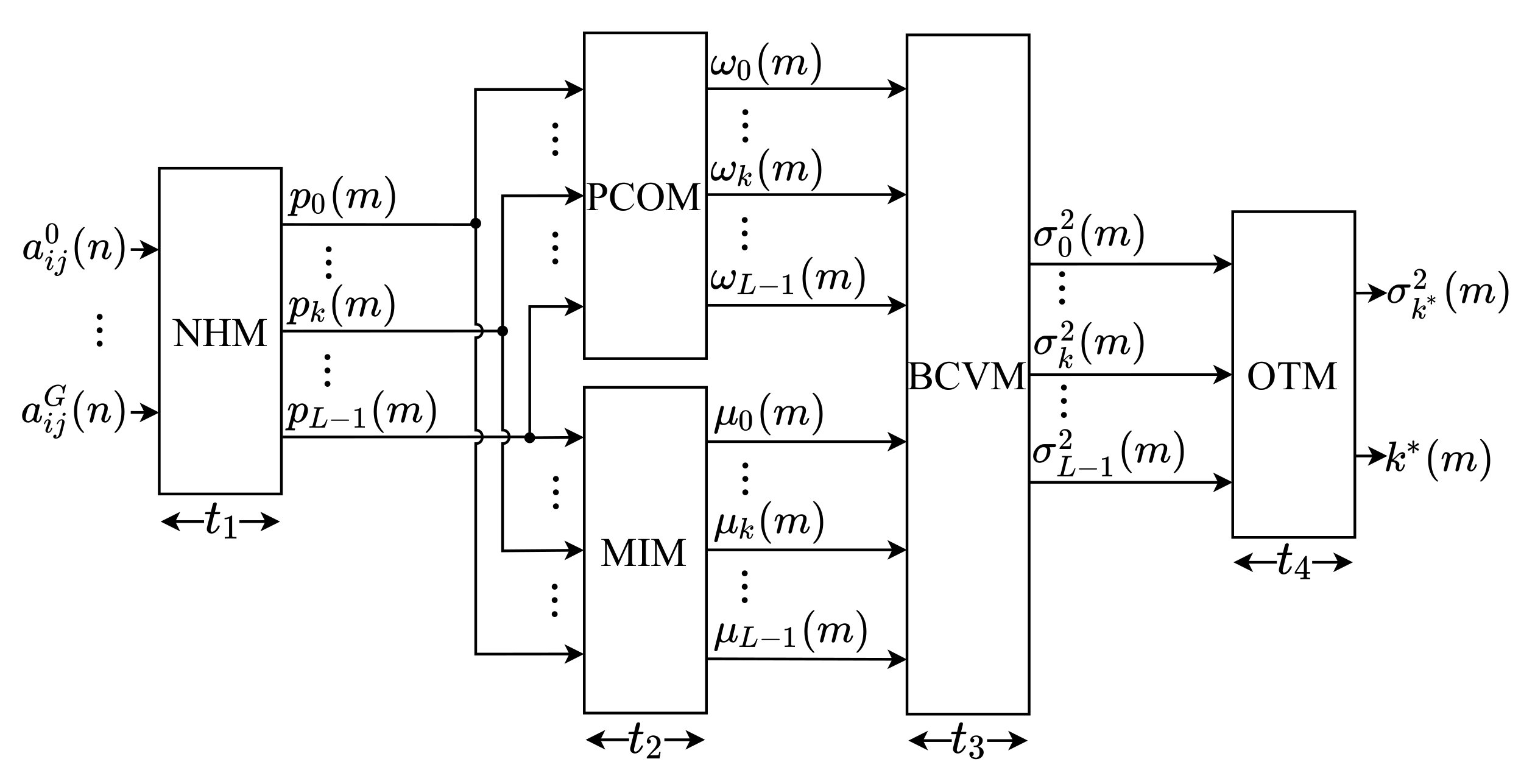
The general hardware architecture implemented for the Otsu algorithm is presented through a block diagram, shown in Figure 1. As can be observed, the architecture was developed based on the description presented in Section 3. Therefore, it consists of five main modules: Normalized Histogram Module (NHM), Probability of Class Occurrence Module (PCOM), Mean Intensity Module (MIM), Between-Class Variance Module (BCVM), and Optimal Threshold Module (OTM).
Initially, the NHM module receives the parallel input of G image pixels, where G is the number of submodules internal to the NHM that simultaneously calculate the normalized histogram, according to Equations (3) and (4). Subsequently, the PCOM module uses the histogram components to calculate the class occurrence probabilities, according to Equation (9), while the MIM module calculates the average intensities, based on Equation (10). The PCOM and MIM modules perform their calculations simultaneously. Afterward, these two modules’ outputs are supplied to BCVM, in which the values of the between-class variance are computed, according to Equation (8). Finally, the calculated between-class variances are compared in the OTM to select the optimal threshold value, as described in Equation (7).
All variables and constants shown in Figure 1 were implemented in fixed point to reduce the bit-width compared to floating-point implementations, the bits number used can be adjusted to adapt the precision of the results obtained to the desired application. Therefore, each pixel, , of the input image were configured with 8 bits in the integer part (without sign), then is defined. For the histogram components, , and the probabilities of class occurrence, , which has a positive value less than 1, only 24 bits are used in the decimal part. For the average intensity elements, , 8 bits are used in the integer part (without sign) and 24 bits in the decimal part. For the between-class variances, , 27 bits are used in the integer part (one bit for sign) and 24 bits in the decimal part. Finally, for the optimal threshold, , only 8 bits are used in the integer part (without sign).
The modules of this architecture are pipelined, and the system operates on the same sample time, . Nonetheless, each module has a different execution time, characterized here as , , and . To minimize control, due to the lack of synchronism between the modules, the hardware proposed here defines , where is the time to process a complete image, being equal to the m-th moment that an image is processed. The time is defined by the NHM block, since has the longest execution time. Thus, the system has an initial latency expressed as
and a throughput characterized as
4.2. Normalized Histogram Module (NHM)
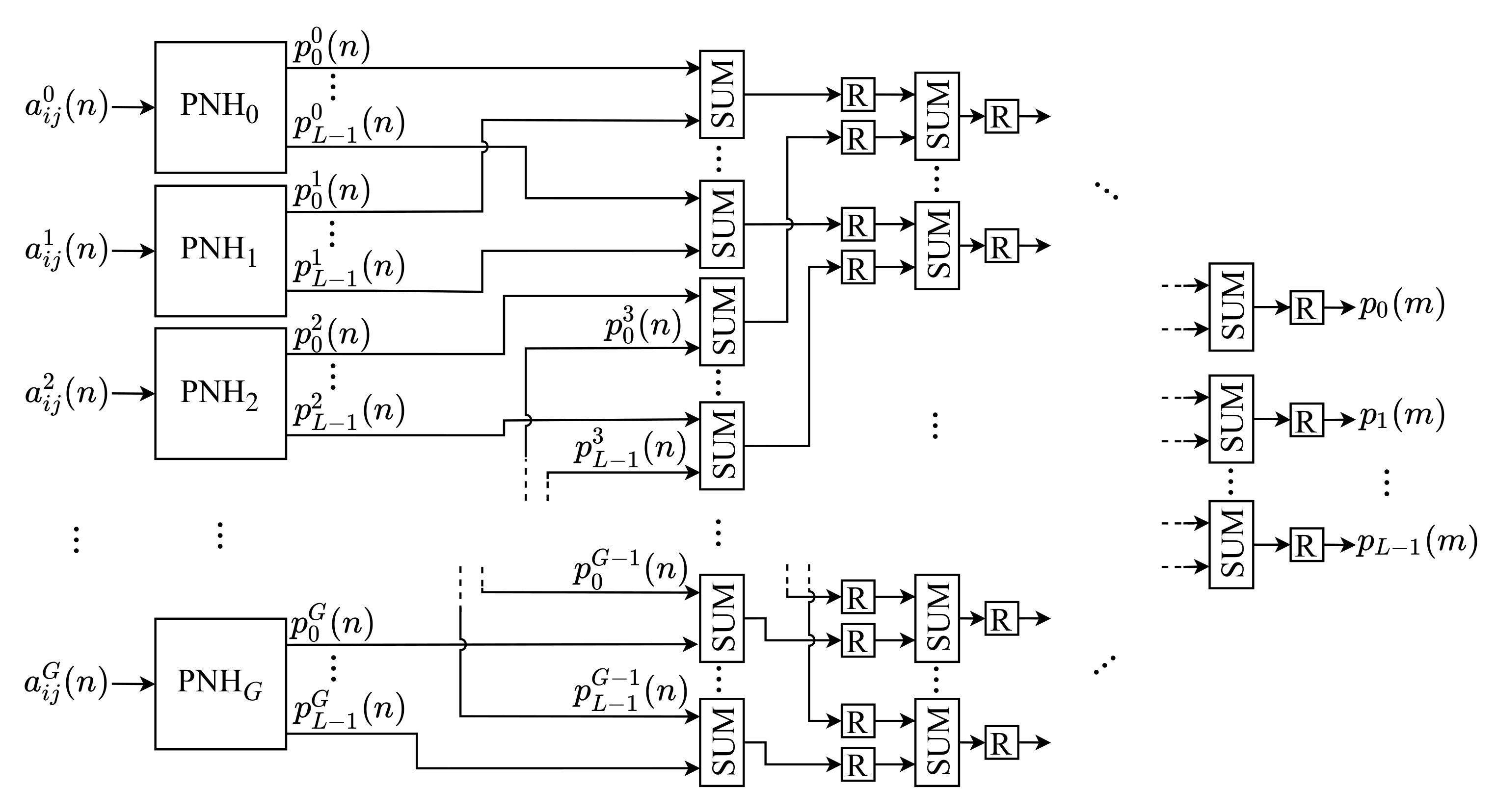
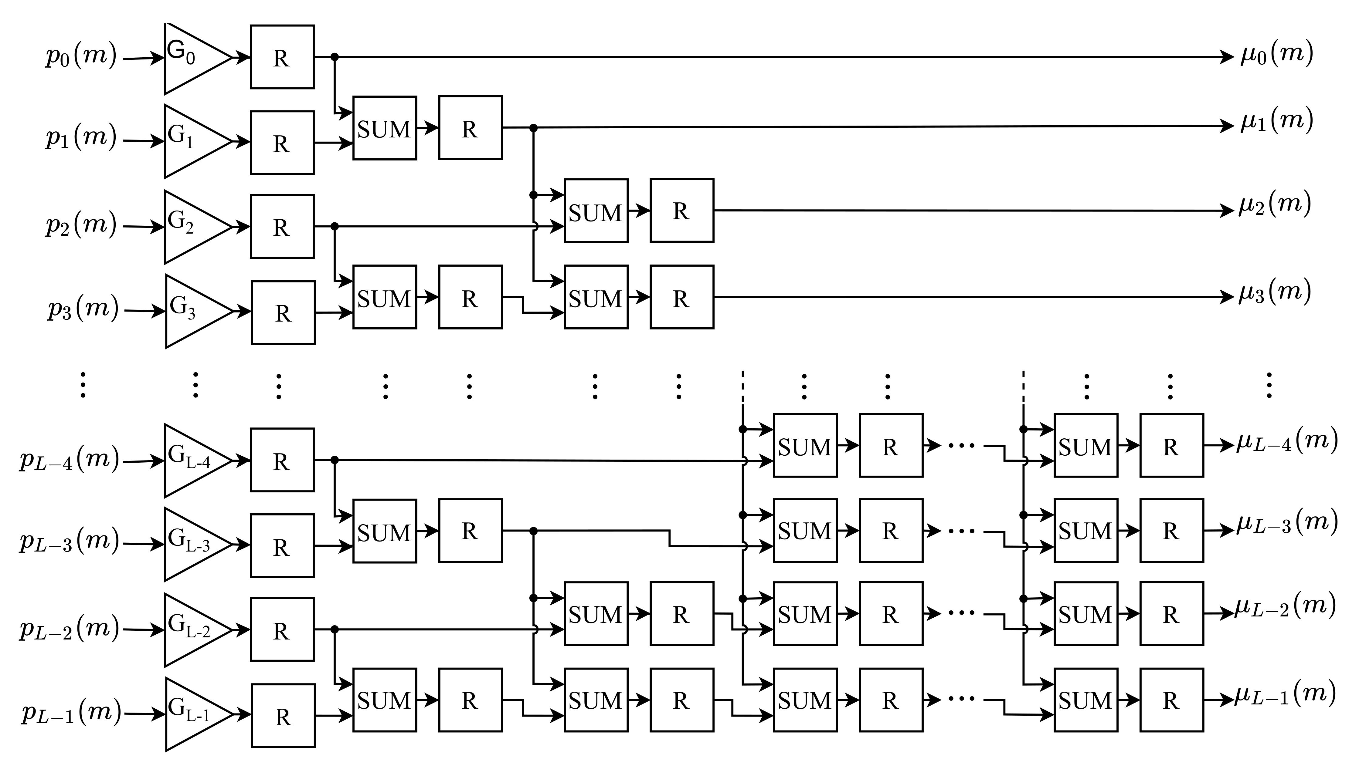
The NHM is responsible for generating the normalized histogram of the input image, by performing the Equations (3) and (4). Usually, this step of the algorithm costs more clock cycles to complete than other steps, as the entire image needs to be scanned to obtain the histogram components. We propose the parallelization of this step by calculating the components’ partial values in a parallel way to optimize this process. Afterward, these values are summed to obtain their final values. The architecture of this module is shown in Figure 2.
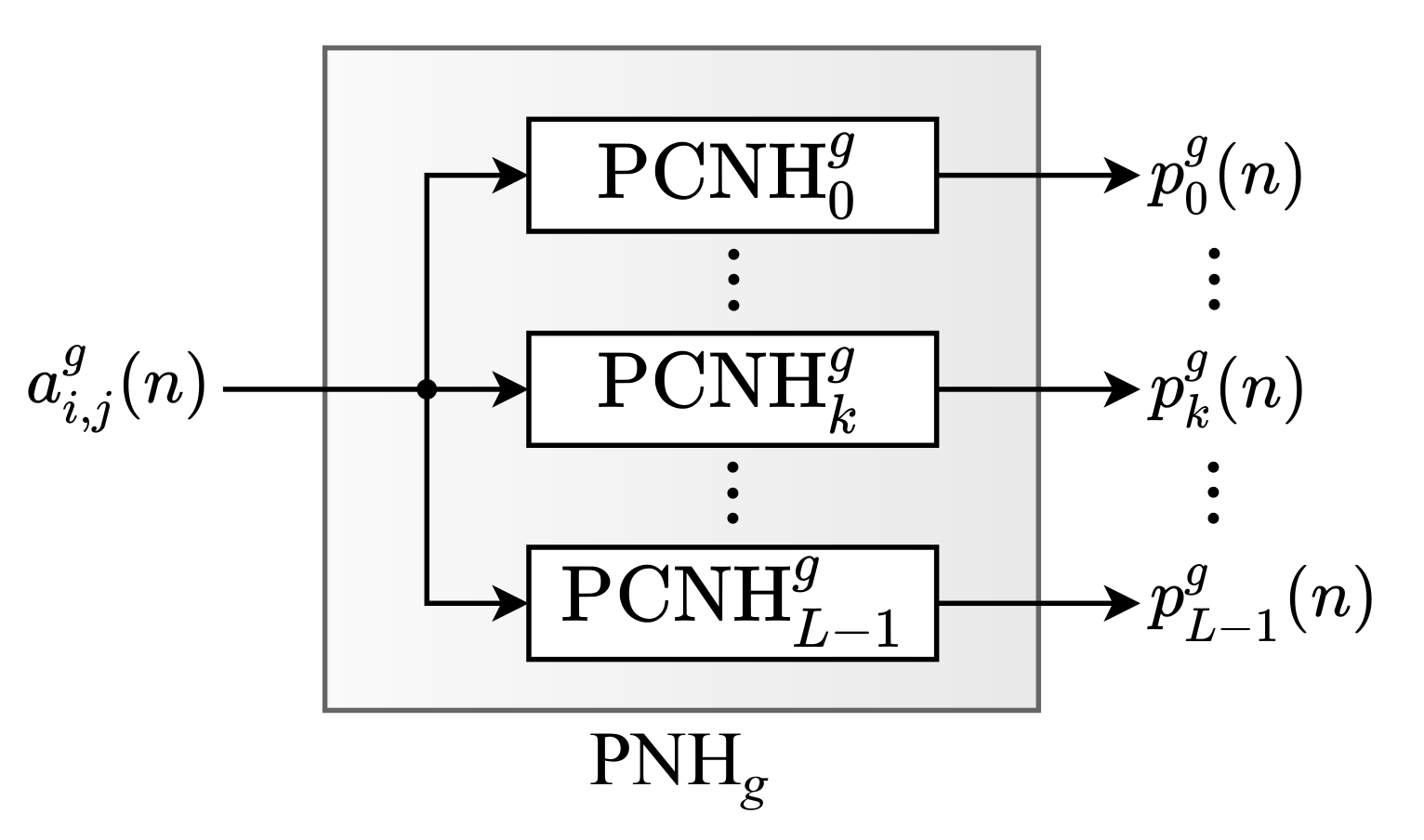
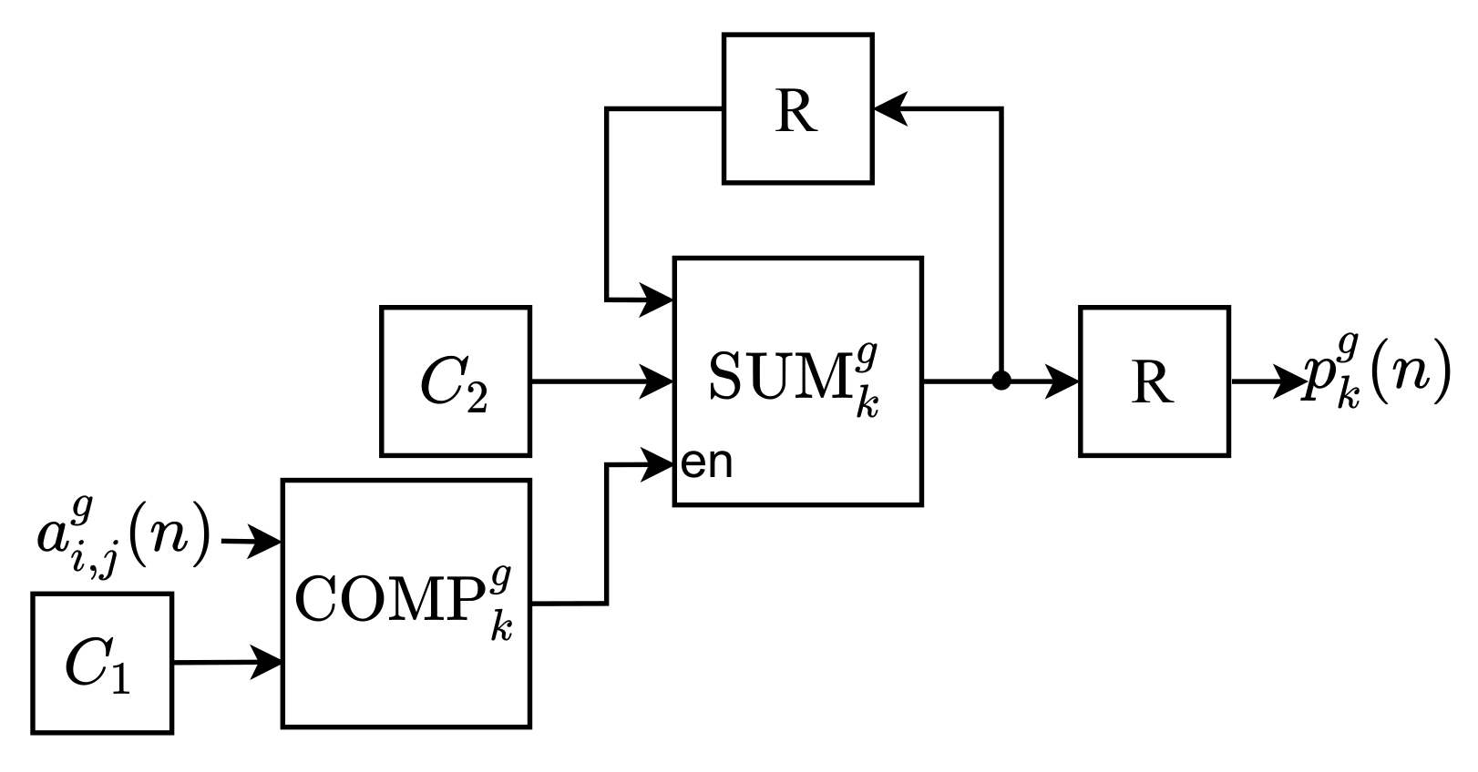
As can be observed, the NHM module is constituted of G identical submodules, called Partial Normalized Histogram (PNH), responsible for computing the partial values of the histogram components. Each g-th input pixel, , is processed by the g-th . Likewise, the PNH modules are internally constituted of L submodules, called Partial Component of the Normalized Histogram (PCNH), as shown in Figure 3. Thus, each k-th partial component of the histogram calculated by the g-th PNH, , is computed in parallel by a submodule. Figure 4 shows the internal circuit of each PCNH module, consisting of a comparator (), an adder (), two registers (R) and two constants ( and ).
Initially, in each k-th comparator of the g-th , , it is checked whether the input pixel, , has value equal to , according to Equation (6). The constant has a different value of k in each submodule. Following, the output, , which is a Boolean value, enables the adder, , when equal to 1. Therefore, when is enabled, the constant is summed with its previous value, thus operating as an accumulator. The constant is defined as , so it determines the value of when summed times, according to Equation (4). After entering all the image pixels, each outputs the k-th partial component of the normalized histogram computed in the g-th PNH, .
After that, the final value of each k-th component of the m-th image, , is obtained by summing all the k-th partial values provided as an output of each g-th PNH, . This sum is performed for each k-th component through an adder tree (), as represented in Figure 2. This tree has a depth equal to . At the end, the value of the components of the normalized histogram, , is obtained, according to Equation (3).
Instead of processing 1 pixel per sample time in the histogram, the proposed architecture allows processing G pixels in parallel. Consequently, the amount of clock cycles required in this step is reduced and, thus, the processing time of a complete image, . Consequently, the latency is also reduced, and throughput increased. With this scheme, the value of can be defined by
Through this equation, it is possible to observe that the higher the value of G, the better the performance obtained.
In each PCNH submodule, the constant assumes a grayscale value between 0 and and is represented with only 8 bits in the integer part (without sign). The constant , which has a positive value less than 1, uses only 24 bits in the decimal part. This bit-width is also used for all the adders of the NHM module, as the normalized histogram components also assume positive values less than 1. All the k-th components of the histogram, , are transmitted in parallel to PCOM and MIM.
4.3. Mean Intensity Module (MIM)
The MIM calculates the average intensity value of the pixels up to level k, according to Equation (10). Each k-th average intensity, , is calculated in parallel. The architecture of this module, shown in Figure 5, consists of L gains submodules (), adders () and one register (R) after each component.
Based on the Equation (10), each k-th component of the normalized histogram is first multiplied by a gain with the value of k. These gains are represented in the architecture block diagram by , and the index indicates the value of the applied gains. Thereafter, each k-th average intensity, , is obtained by summing the outputs of all gains with an index from 0 to k. The sum of these values is carried out in parallel based on the adder proposed by [28], with a maximum of cascading adders using this technique.
All k-th gains of this module, , have their output represented with 8 bit in the integer part (without sign) and 24 bits in the decimal part. Similarly, this bit resolution is also used for the adders, , as the average intensity values of the pixels are at most equal to , for input images with pixels represented by 8 bits. All k-th average intensities, , are provided to BCVM in parallel.
4.4. Probability of Class Occurrence Module (PCOM)
The probability of class occurrence for a given threshold k, , is performed in PCOM based on Equation (9). This module has an architecture similar to MIM, but it does not have the gain submodule to weight the input. Therefore, the inputs are directly linked to the adders (). Thus, this architecture is composed only of adders and registers, as shown in Figure 5.
According to Equation (9), the values are obtained by adding all the components of the histogram from index 0 to k. Thus, using the parallel adder proposed by [28], all values are computed simultaneously through the sum of the k-th entries .
The adders in this module were implemented for the same bit resolution of the inputs, , since the probability of class occurrence also assumes positive values less than 1. All k-th probabilities calculated are propagated to the BCVM in parallel.
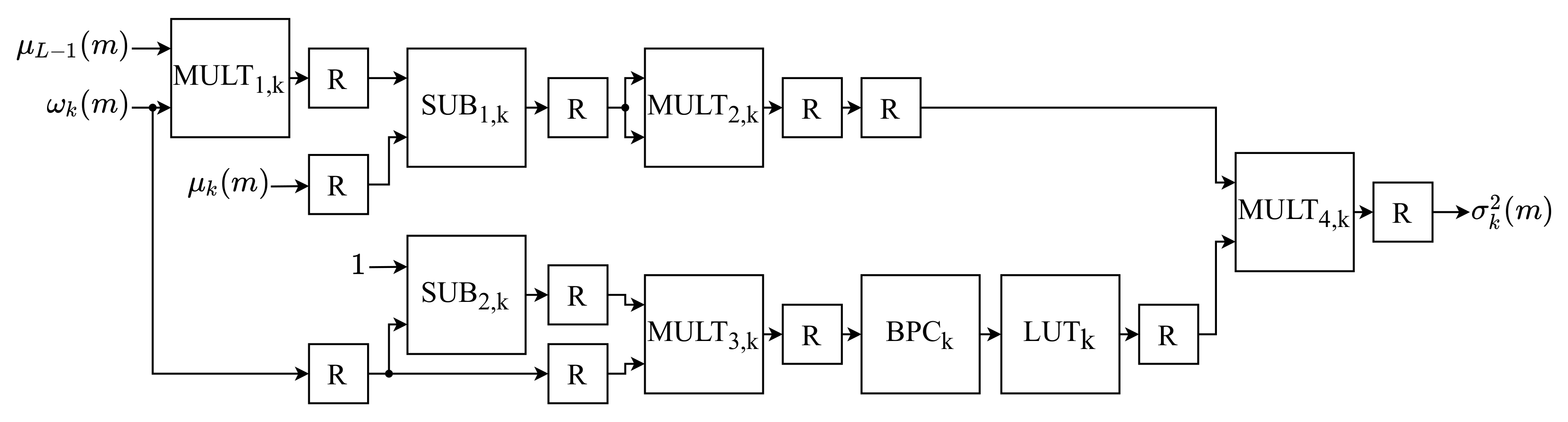
4.5. Between-Class Variance Module (BCVM)
The k-th between-class variance of the m-th image, , are calculated by BCVM based on the Equation (8). The BCVM module is internally composed of L equal submodules, named Between-Class Variance of k (), with the same architecture shown in Figure 6. Each k-th is computed in parallel by the k-th submodule . This submodule consists of four multipliers (), two subtractors (), a point shift (), a Look-Up Table () and eleven registers (R).
Equation (8) is performed in parallel in this architecture. Therefore, the numerator and denominator are performed simultaneously. Concerning the numerator, it is obtained by first multiplying the k-th probability, , by the global mean, , on . Subsequently, the k-th submodule performs the subtraction between and the output. Finally, the result of this subtraction is multiplied by itself in the k-th . Regarding the denominator, it is calculated by initially subtracting the k-th probability, , from the value 1 in the k-th . Lastly, the result is multiplied by the same in the k-th .
The division arithmetic operation is highly costly to the hardware in terms of processing speed, being the architecture’s bottleneck due to the highest critical time. One way to avoid using the division is to multiply the numerator by the reciprocal of the denominator. By definition, the reciprocal of a number is its inverse. Thereupon, the denominator’s reciprocal can be approximated for a range of predefined values and stored in a LUT. Thus, the division can be performed using only one LUT and a multiplier, and , consequently increasing the throughput of the implementation.
Thus, each k-th value in the output of has a reciprocal approximated value in the k-th . This LUT was configured with a depth of L, storing words of 33 bits, where 9 bits represent the integer part (one bit for sign) and 24 bits the fractional. The mapping of the output value of each k-th to an address of the is performed by shifting the binary point eight bits to the right by the k-th . The approximate value of the reciprocal shown at the output of each k-th is multiplied by the calculated value of the numerator in . The result of this multiplication is the k-th between-class variance of the m-th image, .
The subtractor was configured with 9 bits in the integer part (one bit for sign) and 24 bits in the decimal part, while , uses only 24 bits in the decimal part. The multiplier uses 8 bits in the integer part (without sign) and 24 bits in the decimal part, while uses 18 bits in the integer part (one bit for sign) and 24 bits in the decimal part. Meanwhile, was configured with only 24 bits in the decimal part, and uses 27 bits in the integer part (one bit for sign) and 24 bits in the decimal part. Each k-th between-class variance calculated is propagated in parallel to the OTM.
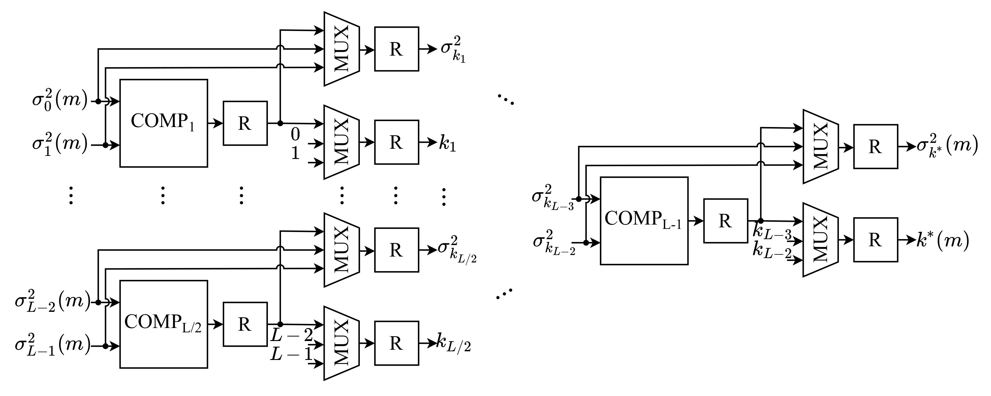
4.6. Optimal Threshold Module (OTM)
The OTM module performs the last step of the Otsu algorithm, responsible for comparing all k-th values of the between-class variance, , to determine the optimal threshold of the m-th image, , based on Equation (7). The architecture of this module is shown in Figure 7. As can be observed, it consists of comparators (), multiplexers () and a register (R) after each component.
According to Equation (7), the optimal threshold of the m-th image, , is the threshold value for which the highest value of between-class variance is obtained. For this purpose, the between-class variances of the m-th image, , are compared through a comparator tree. Each k-th compares whether a given variance is greater than the other, . This comparator is used as a key selector of two multiplexers, defining on the outputs the largest variance value that was compared and its respective threshold k. All outputs of the multiplexers are passed to the next branch of the tree until the last comparator, , in which the optimal threshold value of the m-th image, , should be selected as the output of the multiplexers, as well as its between-class variance, .
Therefore, the optimal threshold of the m-th input image is determined by the proposed architecture of a fully parallel design. A new value of is computed for every m-th instant.
5. Results
The architecture presented in the previous section was developed on an FPGA Arria 10 GX 1150, and the analysis of the synthesis results was carried out concerning hardware area occupation, throughput, and power consumption.
5.1. Hardware Area Occupation Analysis
Initially, the hardware area occupation analysis was performed for the architecture with one PNH module only. The results are shown in Table 1. The first to the third columns indicate the number of logical cells occupied (), the number of multipliers implemented using DSP blocks (), and the number of block memory bits (), respectively. It also presents the resources used in percentage.
As can be observed, only of the block memory bits available have been used, while of the logic cells were occupied. The most-used resource was the multipliers, occupying of the total DSPs available. Therefore, the data presented in Table 1 demonstrate the feasibility of implementing the proposed architecture in the target FPGA. Besides, the Arria-10 FPGA still has resources available that can be used to implement additional logic, thus allowing an increase in the number of PNH modules.
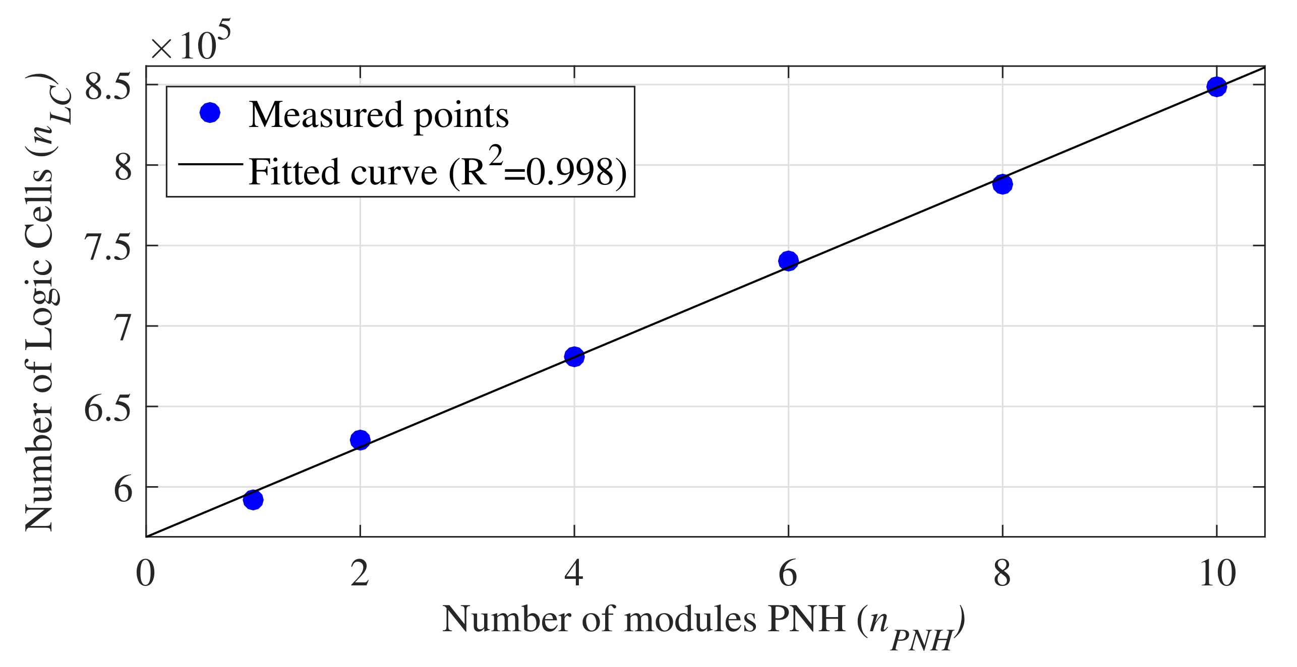
PNH modules require only logical cells for their implementation since they are not designed with multipliers and memories. Therefore, the of unused logic cells in the Arria-10 allow for the increasing of the number of PNH modules. Hence, we also analyzed the area occupation for the Arria-10 FPGA by increasing the number of PNH modules (). The number of occupied logical cells is presented in Table 2, as there is no change in the use of other resources.
Figure 8 shows the curve obtained by linear regression using the set of values presented in Table 2. The equation associated with the regression analysis is expressed by
This equation can obtain the number of logical cells occupied by the architecture without the NHM module when defining .
Therefore, Equation (14) allows for the estimation of the maximum number of PNH modules an FPGA can support. Table 3 presents the maximum number of PNH modules supported on different commercial FPGAs [29,30]. The first and second columns present the label and FPGA, respectively, while the third and fourth columns present the number of logical cells available () and the maximum number of PNH modules that can be implemented with these resources (). Hence, a high degree of parallelism can be achieved through our proposed architecture, limited only by the FPGA resources available.
5.2. Time Processing Analysis
The data related to the system’s processing time was obtained considering a clock cycle of ns, which is defined by its critical path. Moreover, as the circuit operates with the same clock, the sampling time is also defined as ns.
The system’s processing time, for different amounts of , is presented in Table 4. The first column indicates the number of . Meanwhile, from the second to fourth columns are shown, respectively, the image processing time, , defined according to Equation (13), the initial system latency, D, according to Equation (11) and the throughput, , which in this work consists of the number of images processed per second (IPS), determined through Equation (12). According to Equation (13), the processing time of an image depends on its size. Thus, the data presented in Table 4 concern the processing of a image with 4K resolution.
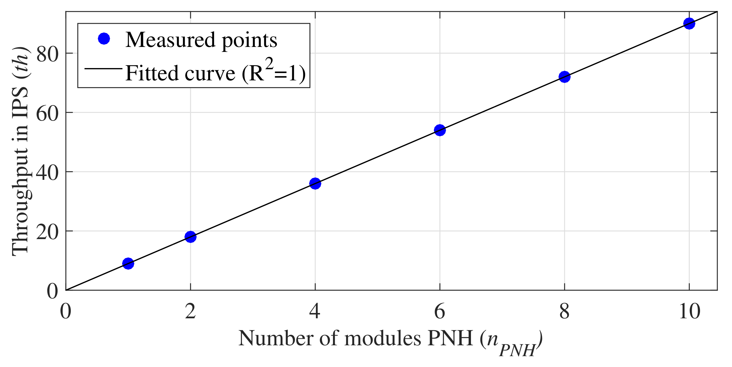
As can be observed in Table 4, the value of is directly proportional to and inversely proportional to and D. Thus, the more PNH modules employed in the implementation, the better the system performance. Figure 9 shows the curve obtained by linear regression that relates the values of and . The equation associated with this curve is expressed by
Equation (16), allows one to define values as
When comparing this equation to Equation (13), it is observed that the only difference between them is the absence of the sum of the logarithm. The reason for that is
Thus, this component can be disregarded in the calculation of .
Afterward, the proposed architecture’s processing time was analyzed for other commercial FPGAs, previously presented in Table 3, adopting for each FPGA an . For this purpose, the values and were defined according to Equations (16) and (17), respectively, and different image resolutions were considered. The results are shown in Table 5.
All FPGA models analyzed achieved a high throughput in processing images with 4 K resolution, allowing real-time processing of 4 K videos in all models. For images with 8 K and 10 K resolutions, real-time processing proved to be more viable in the FPGA2 and FPGA3. Finally, a high throughput was also achieved by the FPGA3 in processing 16 K images, allowing real-time processing of videos with this resolution. Therefore, the FPGA3 offers better performance due to the high number of PNH modules that can be implemented, i.e., the increased architecture’s parallelism.
6. Comparison with State-of-the-Art Works
Comparisons with the state-of-the-art works were performed for the three commercial FPGAs previously mentioned. The architectures were implemented using the maximum number of PNH modules, presented in Table 3. The results were compared only with works that presented data about hardware area occupation and processing time.
6.1. Hardware Occupation Comparison
Table 6 presents the comparison of the hardware area occupation. The first column indicates the reference analyzed. The second to fifth columns show the FPGA, the number of logical cells, multipliers, and the number of bits of memory blocks, respectively, of the reference. Meanwhile, the last four columns present the commercial FPGA to be compared and the ratio between the hardware components used in our proposed implementation, , and those used in the literature, . The ratio of the hardware occupation can be expressed as
where and can be replaced by , , or . This ratio was calculated using the hardware occupancy data presented in Table 1 and Table 3.
The proposal presented by [21] was deployed on a Spartan-6 LX45 FPGA and occupied an area of 1859 LUTs and 44 RAM blocks. This FPGA uses about logic cells (LC) per LUT, having used about LC, and each block of RAM has 18 Kbits, so 792 Kbits of memory is used [31]. The number of multipliers used was not available.
In [19], results were presented for two different implementations of the Otsu method, deployed on the Altera Cyclone IV EP4CE115F29C6N FPGA. The comparison with this work was performed considering the best results presented by its authors, i.e., the method using logarithmic functions. The implemented hardware used 2440 LC, Kbits of memory and 46 multipliers.
The proposal presented in [20] uses the Virtex-5 xc5vfx70tffg1-136-1 FPGA and occupied a total of 161 slices, 4 BRAMs and 5 multipliers. Each slice of this FPGA has 4 LUTs of 6-input, hence, LC per slice was used, and each memory block has 36 Kbits [32]. Thus, about 1030 LC and 144 Kbits of memory were used.
Through Table 6, we found that in all comparisons performed our design presented a more significant hardware area occupation, due to the high degree of parallelism adopted in our proposed implementation, which results in more hardware resources.
6.2. Time Processing Comparison
Table 7 presents a throughput comparison. The analysis was carried out for all the commercial FPGAs previously presented. As can be seen, the first column presents the analyzed reference, while the second to fourth columns show the image resolution (IR), the clock (Clk), and the throughput achieved (), respectively, by the reference. The last three columns indicate, respectively, the FPGAs analyzed, the throughput (), and speedup reached with our architecture. The values of are calculated according to Equation (16), employing the same clock and image size adopted by the compared reference. The speedup calculation is defined as
In [21], the runtime results are presented using a clock of 10 ns and a input image, with pixels represented by 8 bits. The processing time is ms, achieving a throughput of IPS.
In [19], time and latency data were presented considering a clock of ns and the processing of a image, also with pixel representation for 8 bits. As the processing time of an image was not presented by the authors, it was estimated as the clock value times the number of cycles required to enter an image and obtain its respective output. The processed image’s input and output are performed serially, requiring clocks cycles to scan the entire image. The latency indicated for the implementation of the Otsu method using logarithmic optimization is equal to 536. Thus, the calculated time for processing an image is equal to ms per image. Hence, achieving a throughput of IPS.
The proposal presented by [20] displays results from throughput for processing a image, with pixels represented by 8 bits, and adopting a clock of ns. The throughput shown indicates the number of megabits processed per second (Mbps), which in turn is Mbps. As each pixel has 8 bits, the number of images processed per second can be obtained by IPS.
According to the results presented in Table 7, our proposed architecture obtained better throughput values than other works in the literature in all comparisons performed. High speedup values were obtained, varying between and . The performance achieved by the developed architecture is mainly due to the high degree of parallelism explored in this proposal, with a focus on parallelizing the calculation of the histogram. In contrast, works in the literature present implementations with a low degree of parallelism and are focused on optimizing the calculation of between-class variance.
6.3. Power Consumption Comparison
Table 8 presents a comparison of our design’s dynamic power consumption compared to other proposals in the literature. The dynamic power consumption can be expressed as
where is the dynamic power consumption, is the number of hardware components, is the frequency and is the supply voltage. The frequency at which a circuit can operate is proportional to the voltage [12,33]. Thus, the Equation (21) can be rewritten as
For all comparisons, the value of was calculated as
Based on the Equation (22), the saved dynamic energy, , can be expressed by
where and are the number of hardware components and clock of literature works, respectively, and and are the number of components and the clock adopted in this work to obtain the same throughput of the reference to which it is being compared.
Table 8 shows that our implementation presents a significant reduction in energy consumption. The results presented indicate an energy saving, regarding works in the literature, between and . This reduction is obtained through the high degree of parallelism of the technique, which allows one to obtain high throughput with the circuit operating at a low clock frequency. Therefore, although the circuit uses many hardware components, the energy consumed is reduced due to the low-frequency operation.
7. Conclusions
This work presented a parallel implementation proposal of the Otsu method in FPGA. The hardware architecture was developed using RTL design and fixed-point representation. All the implementation details were presented, and the synthesis results were related to the hardware area occupation and processing time. The results showed that the proposed architecture achieved high throughput, enabling real-time processing of high-resolution videos. Comparisons with state-of-the-art works were also performed regarding the hardware area occupancy, throughput and dynamic power consumption. Our proposed architecture outperformed the compared ones in terms of throughput and power consumption, achieving a speedup from until and reducing the power from until . However, the amount of hardware resources required is higher than in other architectures due to the high degree of parallelism adopted in our method. Finally, as future work, a study will be carried out to analyze the impact on the result’s accuracy by reducing the number of bits used. Besides, tests will be conducted with the processing of videos in real-time.
Author Contributions
All the authors have contributed in various degrees to ensure the quality of this work. (e.g., W.K.P.B. and M.A.C.F. conceived the idea and experiments; W.K.P.B. and M.A.C.F. designed and performed the experiments; W.K.P.B., L.A.D. and M.A.C.F. analyzed the data; W.K.P.B., L.A.D. and M.A.C.F. wrote the paper. M.A.C.F. coordinated the project.). All authors have read and agreed to the published version of the manuscript.
Funding
This study was financed in part by the Coordenação de Aperfeiçoamento de Pessoal de Nível Superior (CAPES)—Finance Code 001.
Acknowledgments
The authors wish to acknowledge the financial support of the Coordenação de Aperfeiçoamento de Pessoal de Nível Superior (CAPES) for their financial support.
Conflicts of Interest
The authors declare no conflict of interest.
References
- Barros, W.K.; Morais, D.S.; Lopes, F.F.; Torquato, M.F.; Barbosa, R.d.M.; Fernandes, M.A. Proposal of the CAD system for melanoma detection using reconfigurable computing. Sensors 2020, 20, 3168. [Google Scholar] [CrossRef] [PubMed]
- Menaka, R.; Janarthanan, R.; Deeba, K. FPGA implementation of low power and high speed image edge detection algorithm. Microprocess. Microsystems 2020, 75, 103053. [Google Scholar] [CrossRef]
- Younis, D.; Younis, B.M. Low Cost Histogram Implementation for Image Processing using FPGA. In IOP Conference Series: Materials Science and Engineering; IOP Publishing: Bristol, UK, 2020; Volume 745, p. 012044. [Google Scholar]
- Sreenivasulu, M.; Meenpal, T. Efficient hardware implementation of 2d convolution on FPGA for image processing application. In Proceedings of the 2019 IEEE International Conference on Electrical, Computer and Communication Technologies (ICECCT), Coimbatore, India, 20–22 February 2019; pp. 1–5. [Google Scholar]
- Altuncu, M.A.; Kösten, M.M.; Çavuşlu, M.A.; Şahın, S. FPGA-based implementation of basic image processing applications as low-cost IP core. In Proceedings of the 2018 26th Signal Processing and Communications Applications Conference (SIU), Izmir, Turkey, 2–5 May 2018; pp. 1–4. [Google Scholar]
- Bailey, D. Design for Embedded Image Processing on FPGAs; Wiley-IEEE, Wiley: Atlanta, GA, USA, 2011. [Google Scholar]
- Gonzalez, R.C.; Woods, R.E. Digital Image Processing, 4th ed.; Pearson: New York, NY, USA, 2018. [Google Scholar]
- Otsu, N. A Threshold Selection Method from Gray-Level Histograms. IEEE Trans. Syst. Man Cybern. 1979, 9, 62–66. [Google Scholar] [CrossRef] [Green Version]
- Gokhale, M.; Graham, P. Reconfigurable Computing: Accelerating Computation with Field-Programmable Gate Arrays; Springer: Dordrecht, The Netherland, 2005. [Google Scholar]
- Vahid, F. Digital Design with RTL Design, Verilog and VHDL, 2nd ed.; John Wiley & Sons: Hoboken, NJ, USA, 2010. [Google Scholar]
- Dias, L.A.; Damasceno, A.M.; Gaura, E.; Fernandes, M.A. A full-parallel implementation of Self-Organizing Maps on hardware. Neural Netw. 2021. [Google Scholar] [CrossRef] [PubMed]
- Silva, S.N.; Lopes, F.F.; Valderrama, C.; Fernandes, M.A. Proposal of Takagi–Sugeno Fuzzy-PI Controller Hardware. Sensors 2020, 20, 1996. [Google Scholar] [CrossRef] [PubMed] [Green Version]
- Torquato, M.F.; Fernandes, M.A. High-performance parallel implementation of genetic algorithm on fpga. Circuits Syst. Signal Process. 2019, 38, 4014–4039. [Google Scholar] [CrossRef] [Green Version]
- Da Costa, A.L.; Silva, C.A.; Torquato, M.F.; Fernandes, M.A. Parallel implementation of particle swarm optimization on fpga. IEEE Trans. Circuits Syst. Ii Express Briefs 2019, 66, 1875–1879. [Google Scholar] [CrossRef] [Green Version]
- Coutinho, M.G.; Torquato, M.F.; Fernandes, M.A. Deep neural network hardware implementation based on stacked sparse autoencoder. IEEE Access 2019, 7, 40674–40694. [Google Scholar] [CrossRef]
- Jianlai, W.; Chunling, Y.; Min, Z.; Changhui, W. Implementation of Otsu’s thresholding process based on FPGA. In Proceedings of the 2009 4th IEEE Conference on Industrial Electronics and Applications, Xi’an, China, 25–27 May 2009; pp. 479–483. [Google Scholar] [CrossRef]
- Tian, H.; Lam, S.K.; Srikanthan, T. Implementing Otsu’s thresholding process using area-time efficient logarithmic approximation unit. In Proceedings of the 2003 International Symposium on Circuits and Systems, Bangkok, Thailand, 25–28 May 2003; Volume 4, p. IV. [Google Scholar] [CrossRef]
- Pandey, J.G.; Karmakar, A.; Shekhar, C.; Gurunarayanan, S. A Novel Architecture for FPGA Implementation of Otsu’s Global Automatic Image Thresholding Algorithm. In Proceedings of the 2014 27th International Conference on VLSI Design and 2014 13th International Conference on Embedded Systems, Mumbai, India, 5–9 January 2014; pp. 300–305. [Google Scholar] [CrossRef]
- Torres-Monsalve, A.F.; Velasco-Medina, J. Hardware implementation of ISODATA and Otsu thresholding algorithms. In Proceedings of the 2016 XXI Symposium on Signal Processing, Images and Artificial Vision (STSIVA), Bucaramanga, Colombia, 31 August–2 September 2016; pp. 1–5. [Google Scholar] [CrossRef]
- Pandey, J.G.; Karmakar, A. Unsupervised image thresholding: Hardware architecture and its usage for FPGA-SoC platform. Int. J. Electron. 2019, 106, 455–476. [Google Scholar] [CrossRef]
- Das, R.K.; De, A.; Pal, C.; Chakrabarti, A. DSP hardware design for fingerprint binarization and thinning on FPGA. Proceedings of The 2014 International Conference on Control, Instrumentation, Energy and Communication (CIEC), Calcutta, India, 31 January–2 February 2014; pp. 544–549. [Google Scholar] [CrossRef]
- Wang, W.; Huang, X. An FPGA co-processor for adaptive lane departure warning system. In Proceedings of the 2013 IEEE International Symposium on Circuits and Systems (ISCAS2013), Beijing, China, 19–23 May 2013; pp. 1380–1383. [Google Scholar] [CrossRef]
- Zhao, J.; Bingqian, X.; Huang, X. Real-time lane departure and front collision warning system on an FPGA. In Proceedings of the 2014 IEEE High Performance Extreme Computing Conference (HPEC), Waltham, MA, USA, 9–11 September 2014; pp. 1–5. [Google Scholar] [CrossRef]
- Alhamwi, A.; Vandeportaele, B.; Piat, J. Real Time Vision System for Obstacle Detection and Localization on FPGA. In Computer Vision Systems; Nalpantidis, L., Krüger, V., Eklundh, J.O., Gasteratos, A., Eds.; Springer International Publishing: Cham, Switzerland, 2015; pp. 80–90. [Google Scholar]
- Ren, X.; Wang, Y. Design of a FPGA hardware architecture to detect real-time moving objects using the background subtraction algorithm. In Proceedings of the 2016 5th International Conference on Computer Science and Network Technology (ICCSNT), Changchun, China, 10–11 December 2016; pp. 428–433. [Google Scholar] [CrossRef]
- Tulasigeri, C.; Irulappan, M. An advanced thresholding algorithm for diagnosis of glaucoma in fundus images. In Proceedings of the 2016 IEEE International Conference on Recent Trends in Electronics, Information Communication Technology (RTEICT), Bangalore, India, 20–21 May 2016; pp. 1676–1680. [Google Scholar] [CrossRef]
- Kim, H.S. FPGA-based of thermogram enhancement algorithm for non-destructive thermal characterization. Int. J. Eng. 2018, 31, 1675–1681. [Google Scholar]
- Ladner, R.E.; Fischer, M.J. Parallel Prefix Computation. J. ACM 1980, 27, 831–838. [Google Scholar] [CrossRef]
- Intel. Intel® Stratix® 10 GX/SX Device Overview. Available online: https://www.intel.com/content/dam/www/programmable/us/en/pdfs/literature/hb/stratix-10/s10-overview.pdf (accessed on 2 January 2021).
- Intel. Intel® Agilex™ FPGAs and SoCs Advanced Information Brief (Device Overview). Available online: https://www.intel.com/content/dam/www/programmable/us/en/pdfs/literature/hb/agilex/ag-overview.pdf (accessed on 2 January 2021).
- Xilinx. Spartan-6 FPGA Configurable Logic Block. Available online: https://www.xilinx.com/support/documentation/user_guides/ug384.pdf (accessed on 13 June 2021).
- Xilinx. Virtex-5 Special Edition. Available online: https://www.xilinx.com/publications/archives/xcell/Xcell59.pdf (accessed on 13 June 2021).
- McCool, M.; Robison, A.D.; Reinders, J. Chapter 2—Background. In Structured Parallel Programming; Morgan Kaufmann: Boston, MA, USA, 2012; pp. 39–75. [Google Scholar]
Figure 1.
General architecture of the proposed Otsu Algorithm implementation.

Figure 2.
Architecture of the NHM.

Figure 3.
Architecture of the .

Figure 4.
Architecture of the .

Figure 5.
Architecture of the MIM.

Figure 6.
Architecture of the submodule.

Figure 7.
Architecture of the OTM.

Figure 8.
Linear regression curve for the hardware area occupation (logic cells) per .

Figure 9.
Throughput in IPS, , per .


Table 1.
Hardware area occupation for .
| 591,946 (69.3%) | 1222 (80.5%) | 2162 K (3.9%) |
Table 2.
Number of logic cells required per PNH module.
| 1 | 591,946 (69.3%) |
| 2 | 629,096 (73.6%) |
| 4 | 680,884 (79.7%) |
| 6 | 740,368 (86.6%) |
| 8 | 788,092 (92.2%) |
| 10 | 848,630 (99.3%) |
Table 3.
Estimated number of PNH modules, , for some commercial FPGAs.
| Label | FPGA | ||
|---|---|---|---|
| FPGA1 | Arria 10 GX 1150 | 854,400 | 10 |
| FPGA2 | Agilex AGF 027 | 1,825,600 | 44 |
| FPGA3 | Stratix 10 GX 10M | 6,932,160 | 227 |
Table 4.
System’s processing time.
| (ms) | D (ms) | (IPS) | |
|---|---|---|---|
| 1 | 110.32 | 441.28 | 9 |
| 2 | 55.16 | 220.64 | 18 |
| 4 | 27.58 | 110.32 | 36 |
| 6 | 18.39 | 73.56 | 54 |
| 8 | 13.79 | 55.16 | 72 |
| 10 | 11.03 | 44.12 | 90 |
Table 5.
Values of and for some commercial FPGAs for different image sizes.
| Image Size | FPGA1 | FPGA2 | FPGA3 | |||
|---|---|---|---|---|---|---|
| (ms) | (IPS) | (ms) | (IPS) | (ms) | (IPS) | |
| 4 K () | 90 | 398 | 2057 | |||
| 8 K () | 22 | 99 | 514 | |||
| 10 K (10,240) | 16 | 74 | 385 | |||
| 16 K (15,360) | 5 | 24 | 128 | |||
Table 6.
Hardware occupation comparison with other works.
| Ref. | FPGAref | FPGAwork | Roccupation | |||||
|---|---|---|---|---|---|---|---|---|
| [21] | Spartan 6 | 2975 | - | 792 K | FPGA1 | ≈ | - | ≈ |
| FPGA2 | ≈ | - | ≈ | |||||
| FPGA3 | ≈ | - | ≈ | |||||
| [19] | Cyclone IV | 2440 | 46 | K | FPGA1 | ≈ | ≈ | ≈ |
| FPGA2 | ≈ | ≈ | ≈ | |||||
| FPGA3 | ≈ | ≈ | ≈ | |||||
| [20] | Virtex 5 | 1031 | 5 | 144 K | FPGA1 | ≈ | ≈ | ≈ |
| FPGA2 | ≈ | ≈ | ≈ | |||||
| FPGA3 | ≈ | ≈ | ≈ | |||||
Publisher’s Note: MDPI stays neutral with regard to jurisdictional claims in published maps and institutional affiliations. |
© 2021 by the authors. Licensee MDPI, Basel, Switzerland. This article is an open access article distributed under the terms and conditions of the Creative Commons Attribution (CC BY) license (https://creativecommons.org/licenses/by/4.0/).
Share and Cite
MDPI and ACS Style
Barros, W.K.P.; Dias, L.A.; Fernandes, M.A.C. Fully Parallel Implementation of Otsu Automatic Image Thresholding Algorithm on FPGA. Sensors 2021, 21, 4151. https://0-doi-org.brum.beds.ac.uk/10.3390/s21124151
AMA Style
Barros WKP, Dias LA, Fernandes MAC. Fully Parallel Implementation of Otsu Automatic Image Thresholding Algorithm on FPGA. Sensors. 2021; 21(12):4151. https://0-doi-org.brum.beds.ac.uk/10.3390/s21124151
Chicago/Turabian StyleBarros, Wysterlânya K. P., Leonardo A. Dias, and Marcelo A. C. Fernandes. 2021. "Fully Parallel Implementation of Otsu Automatic Image Thresholding Algorithm on FPGA" Sensors 21, no. 12: 4151. https://0-doi-org.brum.beds.ac.uk/10.3390/s21124151
Note that from the first issue of 2016, this journal uses article numbers instead of page numbers. See further details here.