
Design and Analysis of the Capacitive RF MEMS Switches with Support Pillars
School of Applied Science and Technology, Hainan University, Haikou 570228, China
*
Author to whom correspondence should be addressed.
Sensors 2022, 22(22), 8864; https://0-doi-org.brum.beds.ac.uk/10.3390/s22228864
Submission received: 23 October 2022
/
Revised: 8 November 2022
/
Accepted: 11 November 2022
/
Published: 16 November 2022
(This article belongs to the Special Issue Microwave Communication and Signal Transmission Based on Antennas and Metamaterials)
Abstract
:Conventional parallel capacitive RF MEMS switches have a large impact during the suction phase. In general, RF MEMS switches have to be switched on and off in a considerably fast manner. Increasing the driving voltage enables fast switching but also increases the impact force, which causes the beam membrane to be prone to failure. In the present study, the addition of two support pillars was proposed for slowing down the fall of the beam membrane based on the conventional RF MEMS parallel switch, so as to reduce the impact velocity. As such, a novel RF MEMS switch was designed. Further, simulation software was used to scan and analyze the positioning and height of the support pillars with respect to electromechanical and electromagnetic performance. The simulation results show that the optimal balance of impact velocity and pull-in time was achieved at a height of 0.8 um, a distance of 10 um from the signal line, and an applied voltage of 50 V. The impact velocity was reduced from 1.8 m/s to 1.1 m/s, decreasing by nearly 40%. The turn off time increased from 3.9 us to 4.2 us, representing an increase of only 0.05%. The insertion loss was less than 0.5 dB at 32 GHz, and the isolation was greater than 50 dB at 40 GHz.
1. Introduction
Due to their low power consumption, high isolation, low insertion loss, and ability to integrate with other electronic devices, RF MEMS (Radio Frequency Micro-Electro-Mechanical System) switches have been receiving increasing attention. Such advantages render RF MEMS switches an attractive alternative to PIN or FET RF switches [1]. RF MEMS switches are widely used in the fields of aerospace [2], radar [3], mobile communications [4], tunable filters [5], phase shift networks [6], and other notable fields. These switches must satisfy stringent reliability requirements of failure-free operation over billions of cycles. However, due to the special structure thereof, such switches are frequently prone to failures.
Long term reliability still remains a matter of concern in the commercial utilization of RF MEMS switches [7]. The reliability of RF MEMS switches is affected by mechanical and electrical phenomena such as stiction [8], fatigue [9], creep [10], impact force [11], residual stresses [12], and dielectric charging [13]. Among all these reliability issues, the presence of impact force is a major problem. Due to the mechanical nature thereof, the impact force during the suction phase of the switch is considerably high, causing the beam membrane to be prone to failure [14]. Although significant efforts have been made to develop materials that can maintain high switching speeds while keeping structural failures low, high impact force remains one of the leading causes of device failure [15]. For capacitive RF MEMS switches, the higher the impact force when the top and bottom electrodes of the switch come into contact, the faster the impact velocity. This results in more damage to the beam of the switch, which leads to a shorter switch life. In practice, there is always a trade-off between impact velocity and pull-in time. The variation of the fall time and impact velocity with the applied voltage was given in a previous study [11]. Common methods of reducing impact velocity include tailoring the shape of the actuation pulse [15], applying step voltage [16], and using charge drive [17]. A number of researchers have achieved significant results by adjusting the shape of the driving pulse to reduce the impact velocity [18]. Despite such efforts, the customized pulse technique can only be applied in relatively slow switches with switching times Ts ≥ 10 us, requiring sufficient time to form an effective pulse train [19]. The use of a charge drive from a constant current source to reduce the impact velocity in previous research [19] resulted in an 80% reduction in the impact velocity with a bias resistance of 33 MΩ, but caused a 182% increase in the switching time.
In the present study, a new method was established for reducing the impact velocity of RF MEMS capacitive switches while keeping the pull-in time essentially unchanged. A new shunt capacitive MEMS switch was designed based on the support pillars being added to both sides of the signal line of the conventional MEMS switch. The effect of the positioning of the support pillars on the pull-in voltage was analyzed, and the effects of different positions and heights of the support pillars on the electromechanical and electromagnetic performance of the MEMS switch were simulated and compared. The new structure proposed in this paper can be used in satellite, mobile phone communication, radar, and other applications requiring high life.
2. Proposed MEMS Switch Model
2.1. Working Principle
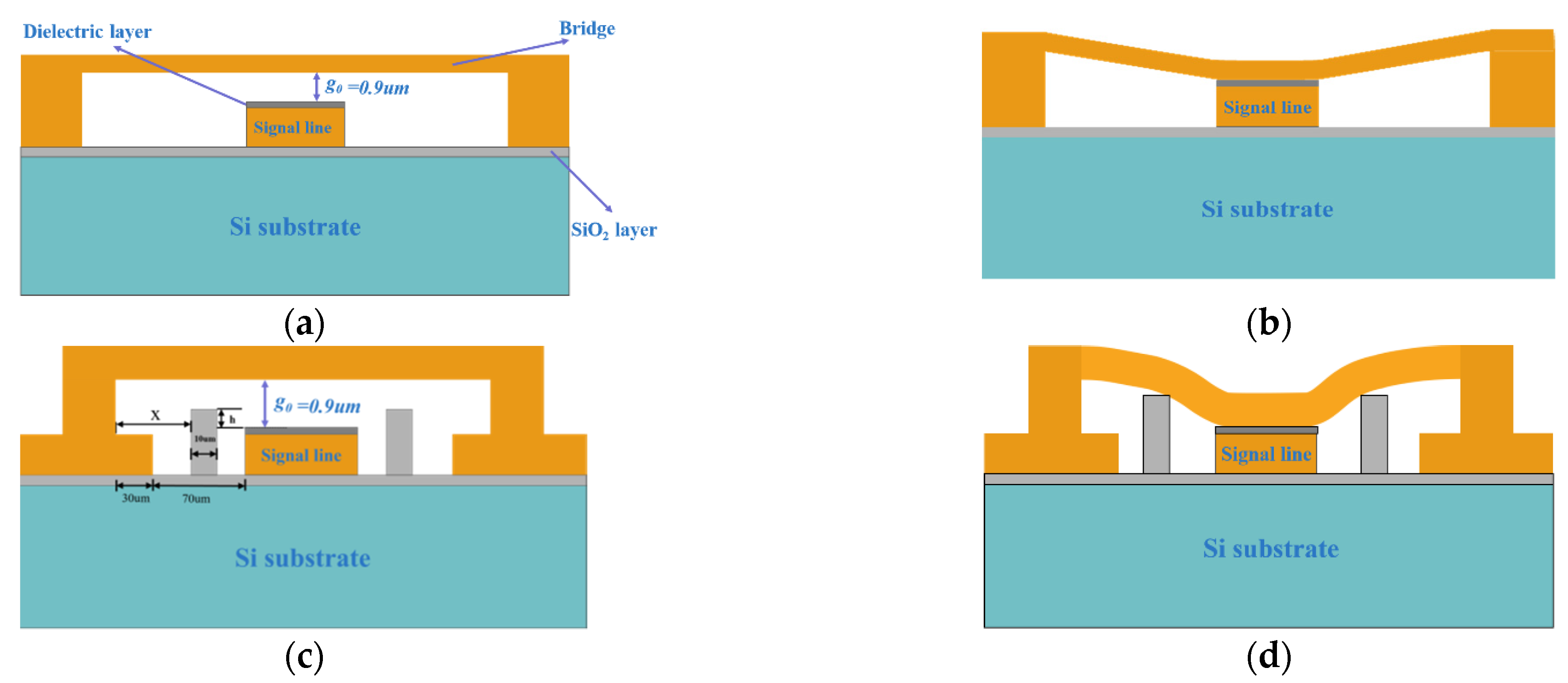
The simplified capacitive RF MEMS switch structure is shown in Figure 1a. The shunt capacitive RF MEMS switch beam is suspended above the signal line at and connected to the left and right sides of the ground line through anchor points. When no driving voltage is applied to the switch, the capacitance between the bridge and the signal line is small, which can be described as denoted in Equation (1) [20]. The microwave signal can hardly be coupled to ground through such capacitance and thus propagates naturally in the waveguide, and the switch is on.
where g0 is the initial distance of the air gap between the top-electrode and the insulating medium; A is the area of driving electrode; is the thickness of the insulating medium film; is the dielectric constant of air; and is the relative dielectric constant of the insulating medium film material.
When a driving voltage is applied between the beam and the bottom-electrode, the bridge is pulled down by the electrostatic force. The capacitance between the bridge and the signal line increases substantially. When the applied driving voltage is greater than a certain critical limit voltage, the electrostatic force overcomes the mechanical stress limit of the beam, causing the bridge to collapse rapidly into contact with the dielectric layer. Here, the microwave signal is coupled to ground through such capacitance, which can be described as denoted in Equation (2) [20]. The signal cannot be transmitted here and the switch is off, at which point the critical voltage is referred to as the pull-in voltage (). We define the time needed for the top electrode to reach the dielectric from its up state position as the pull-in time, and the velocity with which the top electrode lands on the dielectric as the impact velocity.
2.2. Figures, Tables and Schemes
Parallel MEMS switches are typically integrated in a coplanar waveguide (CPW) or microstrip lines, being a surface strip transmission line formed by a central signal line and two ground electrodes extending in parallel on the immediate sides thereof. The signal line and the ground electrode are located on the same surface of the substrate. The center of the signal line is covered with a dielectric layer with a thickness of and a dielectric constant of . To improve the adhesion of the metal to the substrate, a 1 um thick SiO2 layer was added between the substrate and the CPW transmission line. The length of the beam is L, the width is w, and the thickness is t. The width of the signal line is W and the gap is G. The top view of the capacitive parallel switch is shown in Figure 2.
The modified structure of the new MEMS switch is shown in Figure 1c,d and Figure 3. Two symmetrical support pillars, which are made of silicon, are added on both sides of the signal line. Although similar to the working principle of the conventional MEMS switch, the difference is that, during the process of applying driving voltage to pull-down the bridge, the bridge first contacts the support pillars to slow down the descent of the bridge before being pulled onto the dielectric layer. The equivalent elastic coefficient of the beam membrane becomes larger and the impact velocity decreases after the beam contacts the support pillars.
The new MEMS switch designed in the present study has high resistance silicon with a relative dielectric constant of 11.9 and a thickness of 300 um as the substrate. The CPW transmission lines, anchors, and the bridge are all made of gold. G/W/G = 70 um/100 um/70 um; the characteristic impedance is 50 Ω. The dielectric layer uses silicon nitride with a thickness of 0.1 um. The material of the support pillars is silicon with a width of 60 um, which should be no less than the width of the beam film in order to effectively support the beam film. There is also a 1 um thick silica buffer between the substrate and the CPW transmission line. The beam film length of the switch is l = 300 um, the thickness t is 2 um, and the gap is 0.9 um. The material parameters of each component of the switch are shown in Table 1.
2.3. Proposed Pull-In Voltage Model
For capacitive MEMS switches as shown in Figure 4, an electrostatic force is generated when the driving voltage is applied between the beam membrane and the pull-down electrode, which can be simplified to a parallel-plate capacitance equivalent model.
The pull-in voltage of MEMS switch can be expressed as follows [21]:
where is the dielectric constant in vacuum; and is the area of the driving electrode. The formula for calculating the switching elastic coefficient can be obtained as follows:
where E is the Young’s modulus of the beam membrane material; w is the width of the beam; t is the thickness of the switch; and l is the length of the beam membrane.
When the load is uniformly applied to the central 1/3 length range of the solid-supported beam, the elasticity coefficient of the switch at this time can be obtained as denoted in Equation (5):
Two support pillars were added to the new MEMS switch. When the beam touches the support pillars during the pull-down process, the support pillars act as the anchor points of the beam, and the length between the support pillars can be equated to the length of the beam membrane. The gap between the beam membrane and the electrode is reduced from the original to h. The equivalent beam membrane length l is reduced so that increases, rendering the beam membrane more difficult to pull-down. The distance between the support pillars and the anchor point is x, as shown in Figure 5.
Then, for the equivalent model, the length of the new beam film is:
Thus, Equations (3) and (5) can be updated as:
As such, for the new MEMS switch, the beam membrane pull-down process can be divided into two parts: the first part refers to before the beam contacts the support pillars, and the pull-in voltage and spring coefficient are the same as those of the conventional MEMS switch. The second part refers to after the beam contacts the support pillars, and the pull-in voltage and spring coefficient are related to the support pillars positioning and height , as shown in Equations (9) and (10):
where g is the descent displacement of the beam membrane; is the positioning of the support pillars; is the distance between the beam membrane and the dielectric layer; and is the height of the support pillars. g < g0 − h indicates that the beam membrane is not in contact with the support pillars, and indicates that the beam membrane is in contact with the support pillars.
Figure 6 depicts the relationship between the support post position , the height , and the pull-in voltage . From Figure 6, the following observation can be made when the positioning of the support pillars is fixed: the larger the height , the larger the gap between the beam film and the dielectric layer, and the larger the pull-in voltage . When the position is increased, the equivalent beam film length decreases and gradually increases. Therefore, in order to ensure the pull-in voltage is within a reasonable range, the positioning and height of the support pillars need to be chosen reasonably.
3. Electromechanical Performance Analysis
Simulation software was used to model and simulate the new MEMS switch. Two support pillars were placed on both sides of the central signal line, as shown in Figure 3. The theoretical value of ranged from 30 um to 90 um. The positions of the support pillars were on both sides of the signal line at 90 um and close to the ground line at 30 um. The height of the support pillars was the equivalent gap after the beam membrane contacted the support pillars, and the theoretical value ranged from 0 um to 0.9 um. If the height of the support pillars was 0 um, the pillars were not in contact with the beam membrane during the pull-down process. If the height was 0.9 um, the pillars were always in contact with the beam membrane and the support pillars became the new anchor points.
Equation (8) shows that when the position of the support pillars changed, the length of the equivalent beam membrane changed and the pull-in voltage would also change. Figure 7 depicts the relationship between the position of the support pillar and the pull-in voltage . The black curve is the theoretical value and the red curve is the simulated value. The distance between the top of the support pillars and the insulating dielectric layer was 0.75 um, but since the effect of the insulating dielectric layer is not considered in Equation (8), the initial distance needed to be added to the height of the insulating dielectric layer by 0.1 um. In the case of = 0.85 um, changing the value of yielded a different pull-in voltage.
As the position increased, the pull-in voltage gradually increased, and the larger was, the faster the pull-in voltage increased, reaching the maximum pull-in voltage at = 90 um. Such findings could be attributed to a larger , indicating that the support column is closer to the centerline. The stronger the hindering effect of the support pillars on the bridge, the larger the equivalent elasticity coefficient of the beam membrane. The more difficulties in pulling down the bridge, the higher the pull-in voltage of the bridge. The indication is that the positioning of the support pillars has a large influence on the driving voltage of the MEMS switch. For the MEMS switch, a suitable pull-in voltage can weaken the ion injection into the dielectric layer to cause shielding failure or adhesion failure [22]. Therefore, suitable support pillar positioning should be selected to keep the pull-in voltage within an acceptable range. The theoretical values in Figure 7 are basically consistent with the simulated data curves, indicating that the equivalent model is physically reasonable.
Figure 8 depicts the falling displacement of the beam membrane at different times. The displacement changed slowly until 3 us, and the falling displacement was about 1/3 of the gap g0 at 3 us. Subsequently, the displacement of the beam membrane increased rapidly and reached the maximum displacement at 3.9 us. The MEMS switch closed completely at 5 us. The simulation performance was as expected, and thus, the simulation software could be used for further analysis.
Figure 9a depicts the impact velocity and descent displacement as a function of time with and without the addition of the support pillars, respectively, with a driving voltage of 50 V. The velocity and displacement of both were the same from 0 to 3 us, indicating that the beam membrane was not in contact with the support pillars. The velocity slowed down and fluctuated around 0.5 m/s after 1 us of contacting the support pillars, and then the velocity increased rapidly. The bridge contacted the dielectric layer at 4.2 us when the instantaneous impact velocity reached a maximum of 1.1 m/s. Compared with the conventional MEMS switch, the pull-in time was only slightly increased, but the impact velocity was significantly reduced. Figure 9b shows that there was a significant difference in the descent displacement after the beam membrane came into contact with the support pillars, which acted as a buffer for the descent of the bridge.
Figure 7 indicates that when the positioning of the support pillars changed, the MEMS switch pull-in voltage also changed. The impact velocity and pull-in time were not only related to the positioning of the support pillars but also to the applied voltage. If the applied voltage was less than the pull-in voltage causing the switch to fail to close, the impact velocity and pull-in time did not exist. As such, a voltage three to four times higher than the pull-in voltage was applied to weaken the effect of different pull-in voltages in order to observe the effect of the change of the support pillar positioning on the impact velocity and the pull-in time. The simulations were performed by applying 45 V and 50 V, respectively, and the height of the support pillars was 0.75 um. Figure 10a shows the variation of the pull-in time by different positions of the support pillars, and Figure 10b shows the variation of the impact velocity by different positions of the support pillars.
The impact velocity and pull-in time of the conventional MEMS switch and the new MEMS switch were considerably close to each other because the obstruction of the beam membrane by the support pillars was considerably small until 30 um. Figure 10a shows that the pull-in time changed only slightly until 80 um, and the time increased significantly afterwards. Figure 10b shows that the impact velocity decreased slightly with the increase in the support pillar positioning until 60 um, while the impact velocity decreased significantly between 60 um and 80 um, compared with the conventional MEMS switch. From the aforementioned analysis, a conclusion can be drawn that the increase in the support pillar position led to an increase in the pull-in time and a decrease in the impact velocity. Therefore, a suitable position can be found where the pull-in time remains the same while the impact velocity decreases significantly. As an example, at x = 80 um, the closing time was 4.2 us and the impact velocity was 1.1 m/s. Compared with the pull-in time of 3.9 us and the impact velocity of 1.8 m/s without the support pillars, the closing time increased by 0.05% and the impact velocity decreased by almost 40%.
As shown in Figure 11, the simulation was repeated several times when the driving voltage was 50 V and the positioning of the support pillars was changed to 80 um to analyze the change of the positioning of the support pillars on impact velocity and pull-in time.
Since the beam membrane did not come into contact with the support pillars during the pull-down process when the height was less than 0.4 um, the impact velocity and pull-in time were basically the same as when no support pillars were added. After 0.5 um, the pull-in time increased gradually with the increase in height. Further, as the height of the support pillars increased, the increase in the pull-in time became increasingly larger. Because the instantaneous velocity change of the bridge contacting with the dielectric layer was significantly large, the simulation results of the impact velocity had some errors due to the limitation of the mesh division accuracy of the simulation. However, an observation can be made from Figure 11 that the overall change of impact velocity after 0.5 um exhibited a decreasing trend. A conclusion can be drawn that the higher the height of the support pillars, the longer the pull-in time and the smaller the impact velocity. Therefore, a suitable height can be found to make the best balance between pull-in time and impact velocity. For instance, for x = 0.8 um, the impact velocity was 0.8 m/s, which was 45% less than 1.8 m/s without the support pillars, and the pull-in time was 4.7 us, which was 0.2% more than 3.9 us without the support pillars.
From the aforementioned analysis, a conclusion can be drawn that the positioning and height of the support pillars had a significant influence on the impact velocity and the pull-in time of the MEMS switch. The closer the positioning of the support pillars to the signal line and the higher the height, the lower the impact velocity and the longer the pull-in time, which is not suitable for high frequency applications. Thus, choosing the right position and height is critical. The positioning and height of the support pillars were not only related to the impact velocity and pull-in time, but also to the electromagnetic performance of the MEMS switch.
4. Electromagnetic Performance Analysis
In the present study, an electromagnetic simulation model of a parallel-connected capacitive RF MEMS switch was constructed. Further, the positioning and height of the support pillars were scanned and optimized by means of simulation software to derive the effect thereof on the electromagnetic performance. A total of nine combinations of x = 70 um, 80 um, and 90 um, and h = 0.7 um, 0.8 um, and 0.9 um were simulated.
As shown in Figure 12, the curves of different heights at the same position approximately overlap, indicating that the height of the support pillars had basically no effect on the electromagnetic performance of the switch. Figure 12a,b shows that the curves of S11 and S21 at = 70 um and = 80 um in the open-state approximately overlap, and the electromagnetic performance became worse at = 90 um. Such results show that the increase in the position of the support pillars decreased the electromagnetic performance of the MEMS switch. An observation can be made that the closer the support pillars are to the center signal line, the larger the S21 in the open-state and the smaller the S21 in the off-state. Such findings can be attributed to the contact between the support pillars and the signal line changing the equivalent capacitance of the MEMS switch, thereby degrading the electromagnetic performance of the switch. Thus, the actual support pillars should not be positioned too close to the center signal line. The influence of the height and position of the support pillars on the electromagnetic performance was considered to be optimal for the MEMS switch at = 80 um and = 0.8 um. The insertion loss was less than 0.5 dB up to 32 GHz, and the isolation was more than 50 dB at 40 GHz. Therefore, the effect of adding the support pillars on the electromagnetic performance of the MEMS switch was considerably small, and the suitable positioning of the support pillars could be selected to weaken the effect thereof. Overall, the proposed scheme of adding the support pillars is practical and feasible.
5. Conclusions
The present study provides a new method for reducing the impact velocity of the MEMS switch. Specifically, two symmetric support pillars were added under the bridge to buffer the beam during the falling process, thus reducing the impact velocity of the MEMS switch. The effect of adding the support pillars on the impact velocity and pull-in time of the MEMS switch was also analyzed, and the positioning and height of the support pillars were scanned and optimized. A conclusion can be drawn that the closer the support pillars are to the signal line and the higher the height, the lower the impact velocity and the longer the pull-in time. The electromagnetic performance of the switch was largely unaffected by the height of the support pillars. However, when the support pillars were considerably close to the signal line, the electromagnetic performance became considerably poor. The influence of the height and positioning of the support pillars on the impact velocity, pull-in time, and electromagnetic performance was found to be reduced by 40% from 1.8 m/s to 1.1 m/s at = 80 um, = 0.8 um, and 50 V applied voltage. The closing time increased from 3.9 us to 4.2 us, which was only 0.05%, the insertion loss was less than 0.5 dB up to 32 GHz, and the isolation degree was more than 50 dB at 40 GHz. The experimental data suggest that the RF MEMS switch designed in the present study has lower impact speed, shorter closing time, and better electromagnetic performance. Among other methods to reduce the impact velocity, the charge drive of the constant current source is used in the literature [2] to reduce the impact velocity by 80%. The switching time increased by 182%. In the literature [3], the impact velocity was reduced by 21.6% by modulating the actuation force with open-loop operations. We provided the method of adding support pillars, which reduced the impact velocity by 40% but increased the pull-in time by 0.05%.
However, the proposed new method is not perfect. The proposed switch reduces the impact velocity and increases the closing time at the same time, although the increased closing time is acceptable. In addition, manufacturing the proposed MEMS switch requires more than one process to manufacture the support column, which means that manufacturing this switch is technically complicated.
Author Contributions
Conceptualization, M.S. and H.F.; methodology, M.S. and H.F.; software, H.F.; validation, J.Z. and H.F.; formal analysis, C.Z.; investigation, J.Z.; resources, M.S.; data curation, M.S.; writing—original draft preparation, H.F.; writing—review and editing, C.Z. and M.S.; visualization, J.Z.; supervision, M.S.; project administration, M.S.; funding acquisition, M.S. All authors have read and agreed to the published version of the manuscript.
Funding
This work is supported by Hainan Provincial Natural Science Foundation of China (No.620RC553) and Research Initiation Fund of Hainan University (No.KYQD(ZR)20062).
Data Availability Statement
Data available on request from the authors.
Conflicts of Interest
The authors declare no conflict of interest.
References
- Deng, Z.; Wang, Y.; Deng, K.; Lai, C.; Zhou, J. Novel High Isolation and High Capacitance Ratio RF MEMS Switch: Design, Analysis and Performance Verification. Micromachines 2022, 13, 646. [Google Scholar] [CrossRef] [PubMed]
- Sastry, D.V.K. Radio Frequency Microelectromechanical Systems in Defence and Aerospace. Def. Sci. J. 2009, 59, 568–579. [Google Scholar] [CrossRef] [Green Version]
- Gopichand, C.; Maity, R.; Maity, N.P.; Srinivasa Rao, K.; Guha, K.; Maity, S.; Eisnawi, A. Design of a Non-uniform Serpentine Asymmetric Cantilever RF-MEMS Shunt Capacitive Switch for RADAR Applications. Trans. Electr. Electron. Mater. 2020, 21, 406–412. [Google Scholar] [CrossRef]
- Zhang, Y.; Gong, Z.; Guo, X.; Liu, Z. A High Linearity SP12T RF MEMS Switch Using Parallel Dual-Cantilevers for 5G and Beyond Applications. IEEE Electron Device Lett. 2018, 39, 1608–1611. [Google Scholar] [CrossRef]
- Guo, X.L.; Sun, C.W.; Bao, Z.H.; Xu, C.; Zhang, G.; Wang, Z.L.; Yin, H.H.; Zhang, X.F.; Jiang, H. Tunable low-pass Ka-band MEMS filter based on Electromagnetic-Bandgap Structure. Sens. Actuators A: Phys. 2016, 247, 83–89. [Google Scholar] [CrossRef]
- Wang, C.S.; Ying, K.; Li, H.H.; Gao, W.; Yin, L.; Wang, M.; Peng, X.L.; Wang, S.X. Electromechanical coupling modelling of distributed MEMS phase shifter for phased array antennas. Int. J. Electron. 2018, 105, 1358–1373. [Google Scholar] [CrossRef]
- Saleem, M.M.; Nawaz, H. A systematic review of reliability issues in RF-MEMS switches. Micro Nanosyst. 2019, 11, 11–33. [Google Scholar] [CrossRef]
- De Wolf, I.; van Spengen, W.M. Techniques to study the reliability of metal RF MEMS capacitive switches. Microelectron. Reliab. 2002, 42, 1789–1794. [Google Scholar] [CrossRef]
- Soma, A.; De Pasquale, G. MEMS mechanical fatigue: Experimental results on gold microbeams. J. Microelectromech. Syst. 2009, 18, 828–835. [Google Scholar] [CrossRef]
- Somà, A.; Saleem, M.M.; De Pasquale, G. Effect of creep in RF MEMS static and dynamic behavior. Microsyst. Technol. 2016, 22, 1067–1078. [Google Scholar] [CrossRef]
- Jain, A.; Palit, S.; Alam, M.A. A Physics-Based Predictive Modeling Framework for Dielectric Charging and Creep in RF MEMS Capacitive Switches and Varactors. J. Microelectromech. Syst. 2012, 21, 420–430. [Google Scholar] [CrossRef]
- Somà, A.; Saleem, M.M. Modeling and experimental verification of thermally induced residual stress in RF-MEMS. J. Micromechanics Microeng. 2015, 25, 055007. [Google Scholar] [CrossRef]
- Van Spengen, W.M.; Puers, R.; Mertens, R.; De Wolf, I. Experimental characterization of stiction due to charging in RF MEMS. In Proceedings of the Digest. International Electron Devices Meeting, San Francisco, CA, USA, 8–11 December 2002; pp. 901–904. [Google Scholar]
- Mirsaeedi, M.; Anis, M. A statistical yield optimization framework for interconnect in double patterning lithography. Microelectron. J. 2011, 42, 1231–1238. [Google Scholar] [CrossRef]
- Spasos, M.; Tsiakmakis, K.; Charalampidis, N.; Nilavalan, R. RF-MEMS switch actuation pulse optimization using Taguchi’s method. Microsyst. Technol. 2011, 17, 1351–1359. [Google Scholar] [CrossRef] [Green Version]
- De Pasquale, G.; Barbato, M.; Giliberto, V.; Meneghesso, G.; Somà, A. Reliability improvement in microstructures by reducing the impact velocity through electrostatic force modulation. Microelectron. Reliab. 2012, 52, 1808–1811. [Google Scholar] [CrossRef]
- Spasos, M.; Nilavalan, R. On the investigation of a reliable actuation control method for ohmic RF MEMS switches. Microelectron. J. 2011, 42, 1239–1251. [Google Scholar] [CrossRef]
- Czaplewski, D.A.; Dyck, C.W.; Sumali, H.; Massad, J.E.; Kuppers, J.D.; Reines, I.; Cowan, W.D.; Tigges, C.P. A Soft-Landing Waveform for Actuation of a Single-Pole Single-Throw Ohmic RF MEMS Switch. J. Microelectromech. Syst. 2006, 15, 1586–1594. [Google Scholar] [CrossRef]
- Spasos, M.; Nilavalan, R. Resistive damping implementation as a method to improve controllability in stiff ohmic RF-MEMS switches. Microsyst. Technol.-Micro-Nanosyst.-Inf. Storage Process. Syst. 2013, 19, 1935–1943. [Google Scholar] [CrossRef] [Green Version]
- Girish Gandhi, S.; Govardhani, I.; Venkata Narayana, M.; Sarat Kumar, K. Design and performance analysis of novel bridge type RF MEMS switch for X-band. Mater. Today: Proc. 2021. [Google Scholar] [CrossRef]
- Kim, J.-M.; Park, J.-H.; Back, C.-W.; Kim, Y.-K. The SiOG-Based Single-Crystalline Silicon (SCS) RF MEMS Switch with Uniform Characteristics. J. Microelectromech. Syst. A Jt. IEEE ASME Publ. Microstruct. Microactuators Microsens. Microsyst. 2004, 13, 1036–1042. [Google Scholar] [CrossRef]
- Wang, L.F.; Tang, J.Y.; Huang, Q.A. Effect of Environmental Humidity on Dielectric Charging Effect in RF MEMS Capacitive Switches Based on C-V Properties. J. Microelectromech. Syst. 2013, 22, 637–645. [Google Scholar] [CrossRef]
Figure 1.
(a) Simplified capacitive RF MEMS switch OFF, (b) RF MEMS Switch ON, (c) The up state of the new RF MEMS switch, (d) The down state of the new RF MEMS switch.
Figure 1.
(a) Simplified capacitive RF MEMS switch OFF, (b) RF MEMS Switch ON, (c) The up state of the new RF MEMS switch, (d) The down state of the new RF MEMS switch.

Figure 2.
MEMS capacitive parallel switch top view.

Figure 3.
Schematic view of the proposed RF MEMS device.

Figure 4.
MEMS Switch Parallel Plate Equivalent Model.

Figure 5.
(a) MEMS Switch Membrane Equivalent Length Model, (b) MEMS Switch Equivalent Pull-in Model.
Figure 5.
(a) MEMS Switch Membrane Equivalent Length Model, (b) MEMS Switch Equivalent Pull-in Model.

Figure 6.
Relationship between position x, height h, and pull-in voltage.

Figure 7.
Influence of position of support pillars on pull-in voltage; the black curve is the theoretical value and the red curve is the simulation value.
Figure 7.
Influence of position of support pillars on pull-in voltage; the black curve is the theoretical value and the red curve is the simulation value.

Figure 8.
Shape of the beam at different instants of time during pull-down.

Figure 9.
(a) Influence of adding support pillars on impact velocity, (b) Influence of adding support pillars on pull-in displacement.
Figure 9.
(a) Influence of adding support pillars on impact velocity, (b) Influence of adding support pillars on pull-in displacement.

Figure 10.
(a) Pull-in time at different positions of the support pillar, (b) Impact velocity at different positions of the support pillar.
Figure 10.
(a) Pull-in time at different positions of the support pillar, (b) Impact velocity at different positions of the support pillar.

Figure 11.
Effect of changing the height of the support pillars on impact velocity and pull-in time.
Figure 11.
Effect of changing the height of the support pillars on impact velocity and pull-in time.

Figure 12.
Variation of the position and height of the support pillars on the electromagnetic performance of the MEMS switch, (a) MEMS open-state S11, (b) MEMS open-state S21, (c) MEMS off-State S11, (d) MEMS off-state S21.
Figure 12.
Variation of the position and height of the support pillars on the electromagnetic performance of the MEMS switch, (a) MEMS open-state S11, (b) MEMS open-state S21, (c) MEMS off-State S11, (d) MEMS off-state S21.


Table 1.
Dimensions of the proposed switch.
| Component | Width (μm) | Depth (μm) | Height (μm) | Material | Dielectric Constant |
|---|---|---|---|---|---|
| Substrate | 300 | 500 | 300 | High Resistivity Silicon | 11.9 |
| Oxide layer | 300 | 500 | 1 | Silicon Dioxide | 4.2 |
| Anchor | 60 | 50 | 1 | Gold | - |
| Ground electrode | 300 | 130 | 2 | Gold | - |
| Signal line | 300 | 100 | 2 | Gold | - |
| Electrode layer | 60 | 100 | 0.1 | Silicon Nitrate | 9.7 |
| Beam | 60 | 400 | 2 | Gold | - |
| Support pillar | 60 | 10 | 2.80 | Silicon | 4.5 |
Publisher’s Note: MDPI stays neutral with regard to jurisdictional claims in published maps and institutional affiliations. |
© 2022 by the authors. Licensee MDPI, Basel, Switzerland. This article is an open access article distributed under the terms and conditions of the Creative Commons Attribution (CC BY) license (https://creativecommons.org/licenses/by/4.0/).
Share and Cite
MDPI and ACS Style
Feng, H.; Zhao, J.; Zhou, C.; Song, M. Design and Analysis of the Capacitive RF MEMS Switches with Support Pillars. Sensors 2022, 22, 8864. https://0-doi-org.brum.beds.ac.uk/10.3390/s22228864
AMA Style
Feng H, Zhao J, Zhou C, Song M. Design and Analysis of the Capacitive RF MEMS Switches with Support Pillars. Sensors. 2022; 22(22):8864. https://0-doi-org.brum.beds.ac.uk/10.3390/s22228864
Chicago/Turabian StyleFeng, Hongbo, Jiabin Zhao, Chengsi Zhou, and Mingxin Song. 2022. "Design and Analysis of the Capacitive RF MEMS Switches with Support Pillars" Sensors 22, no. 22: 8864. https://0-doi-org.brum.beds.ac.uk/10.3390/s22228864
Note that from the first issue of 2016, this journal uses article numbers instead of page numbers. See further details here.