
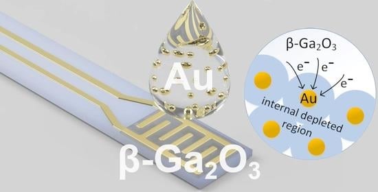
P-type Inversion at the Surface of β-Ga2O3 Epitaxial Layer Modified with Au Nanoparticles

 , , , and
Abstract
:
1. Introduction
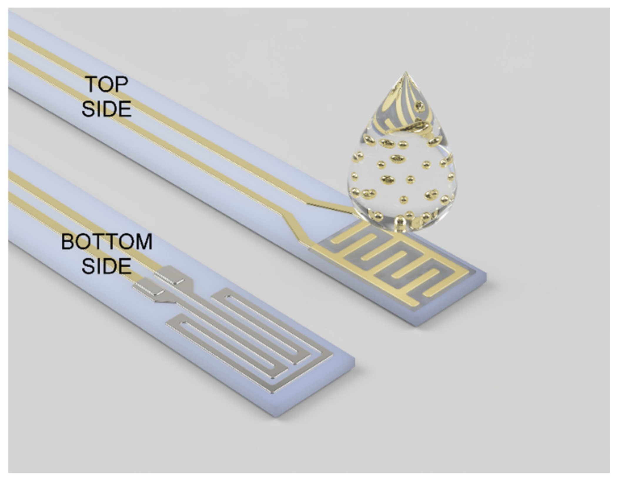
2. Materials and Methods
3. Results
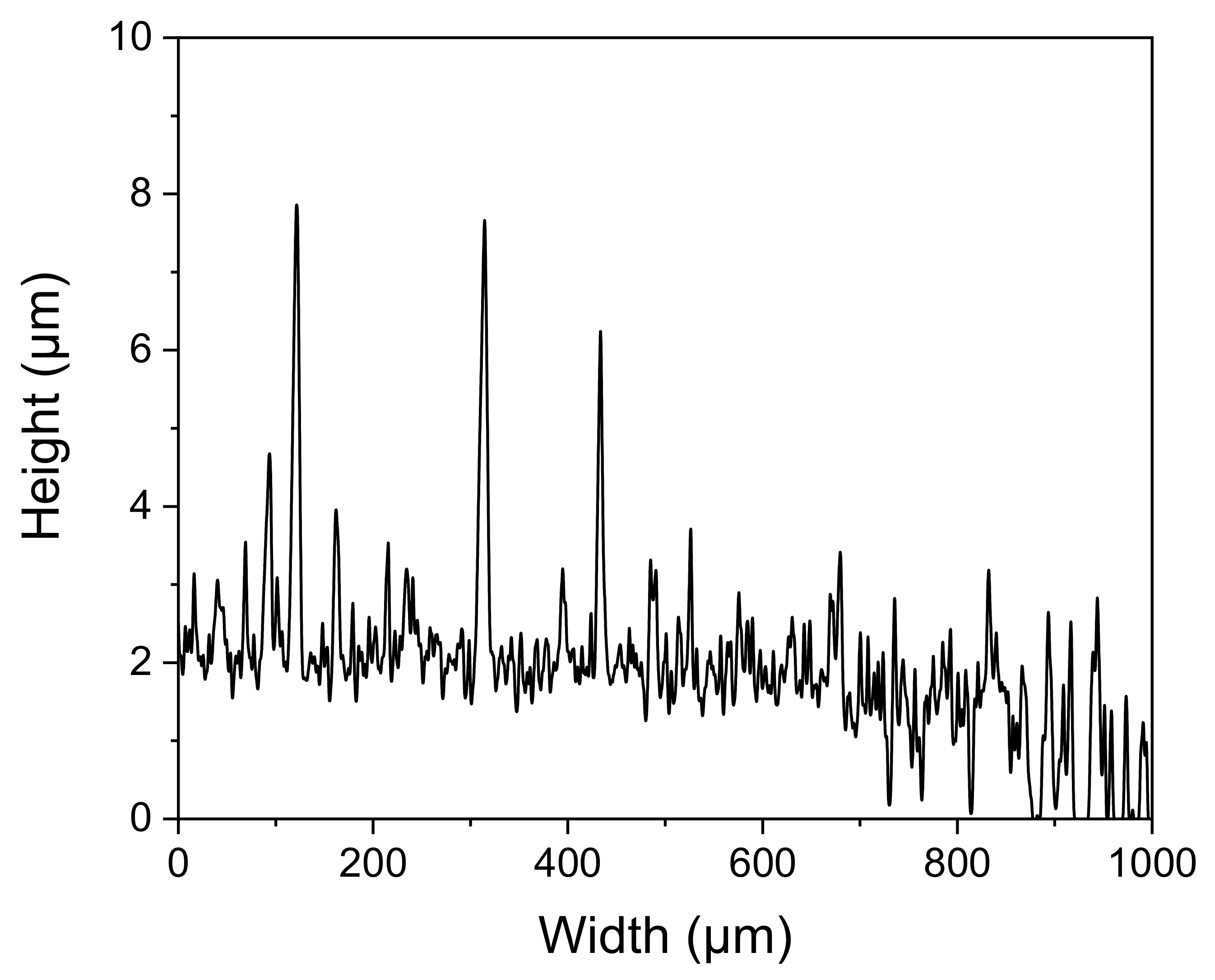
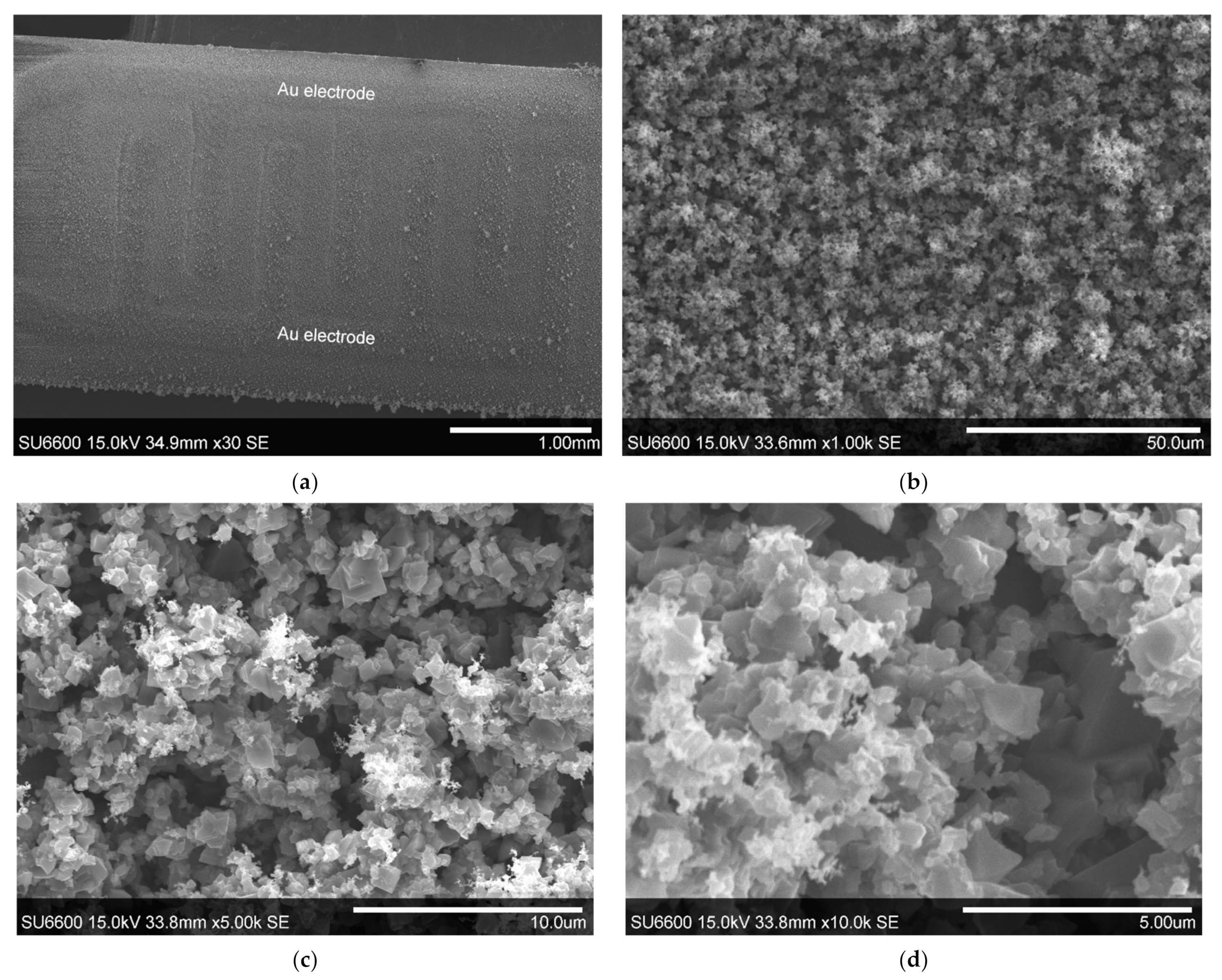
3.1. Microstructure
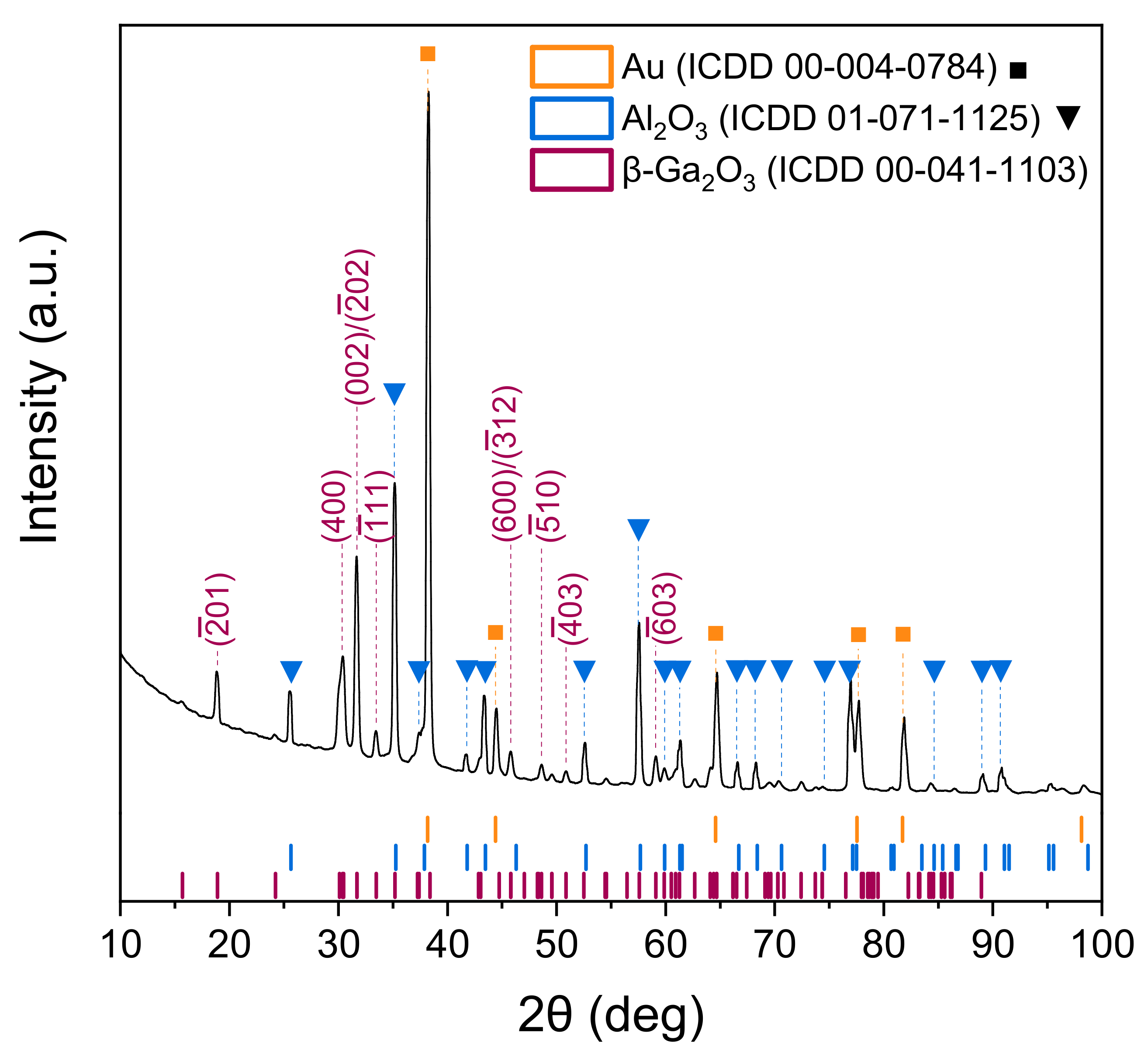
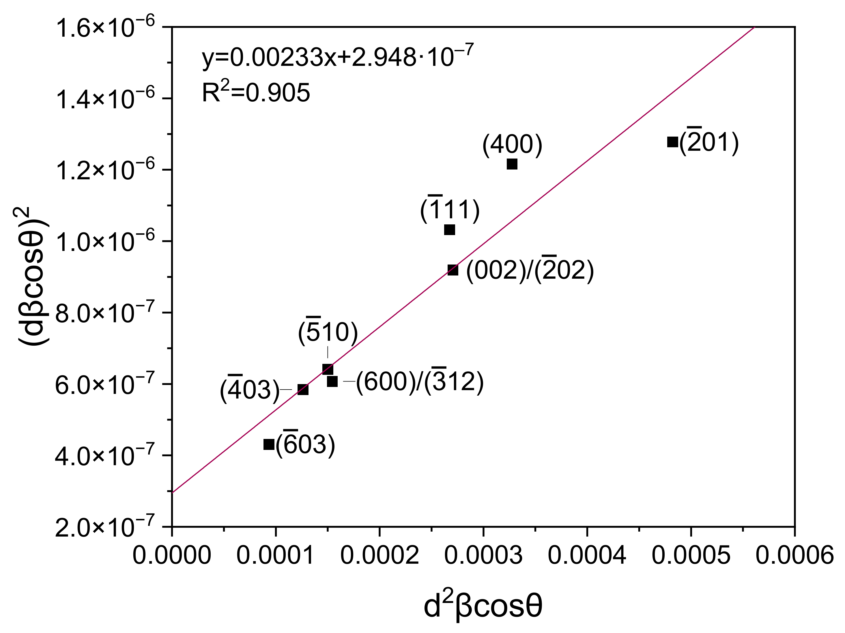
3.2. Crystal Structure
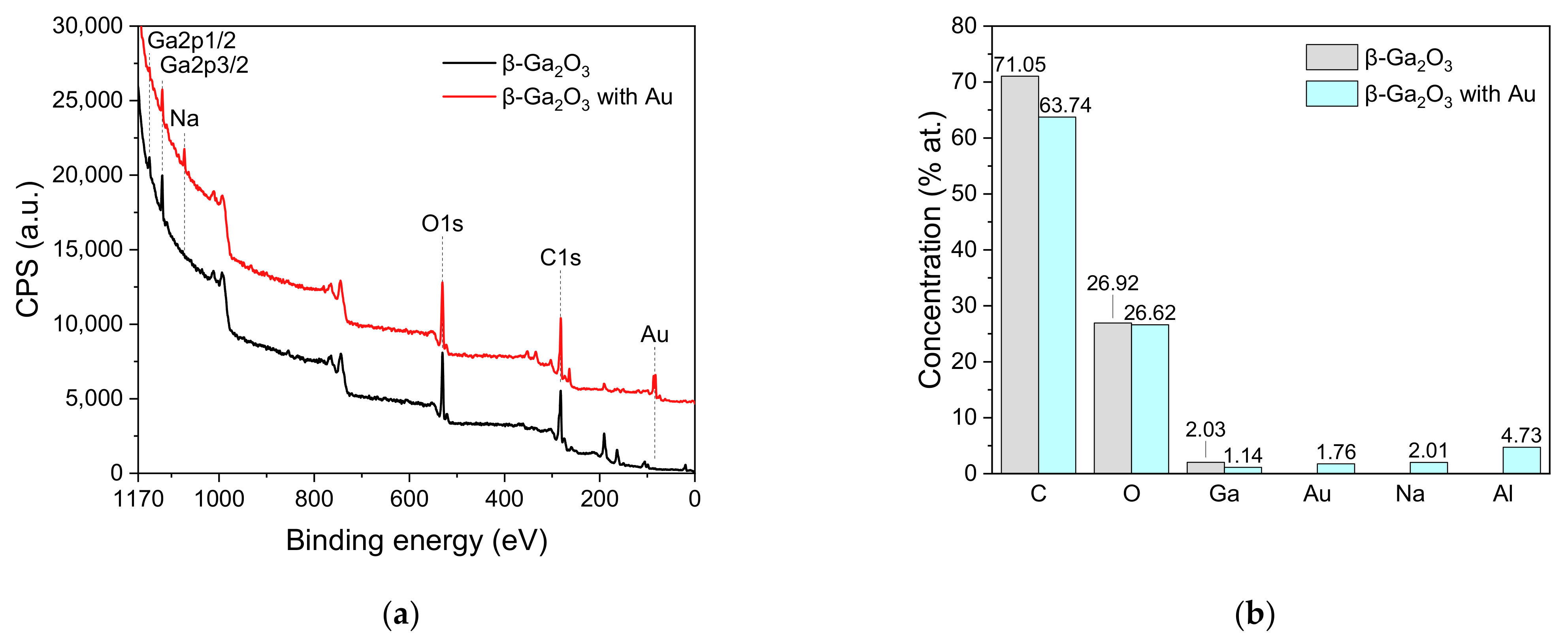
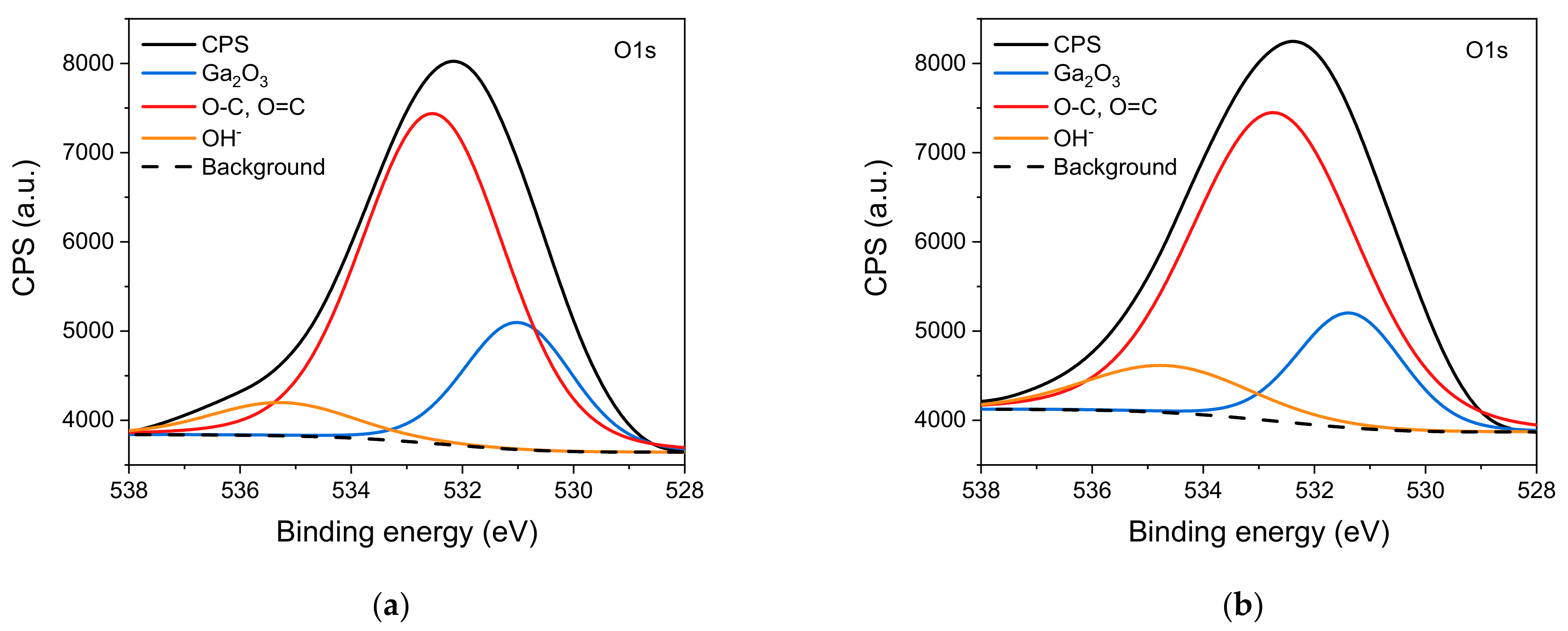
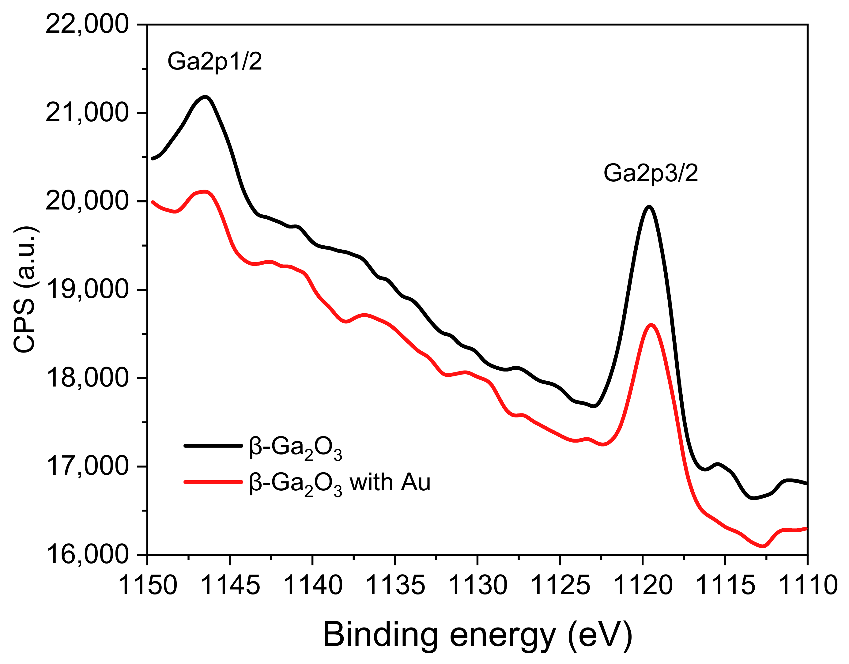
3.3. Chemical Composition of the Surface
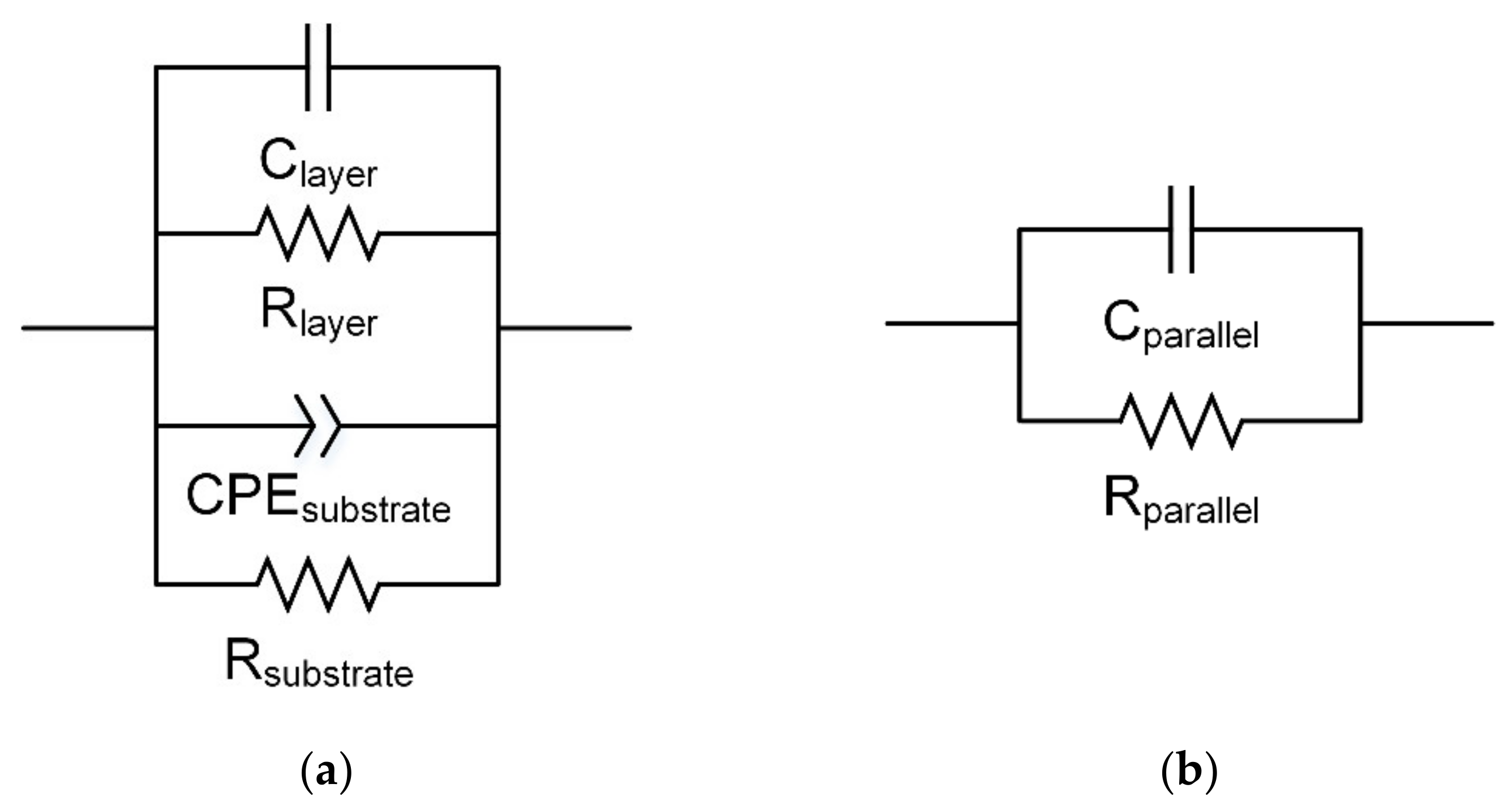
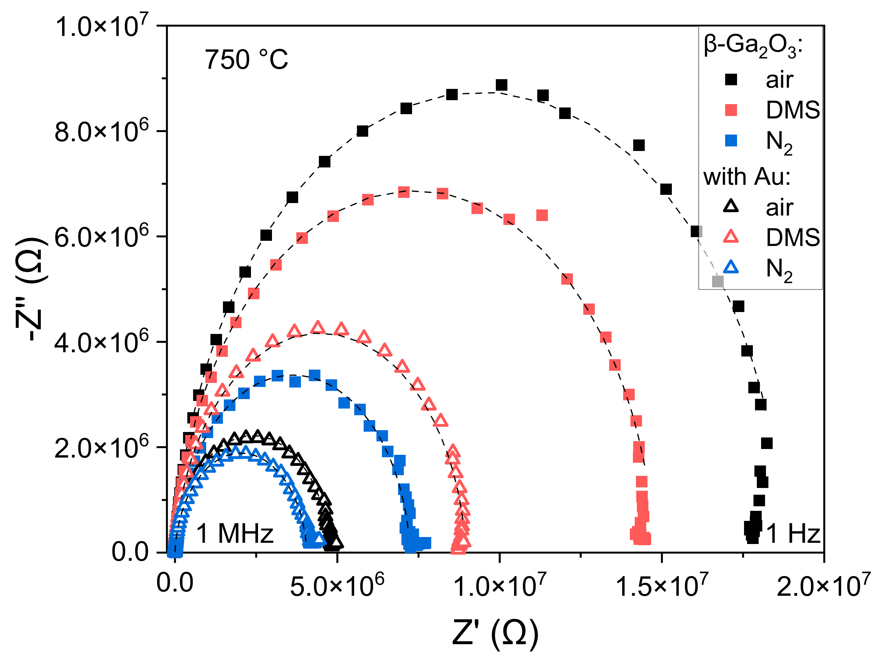
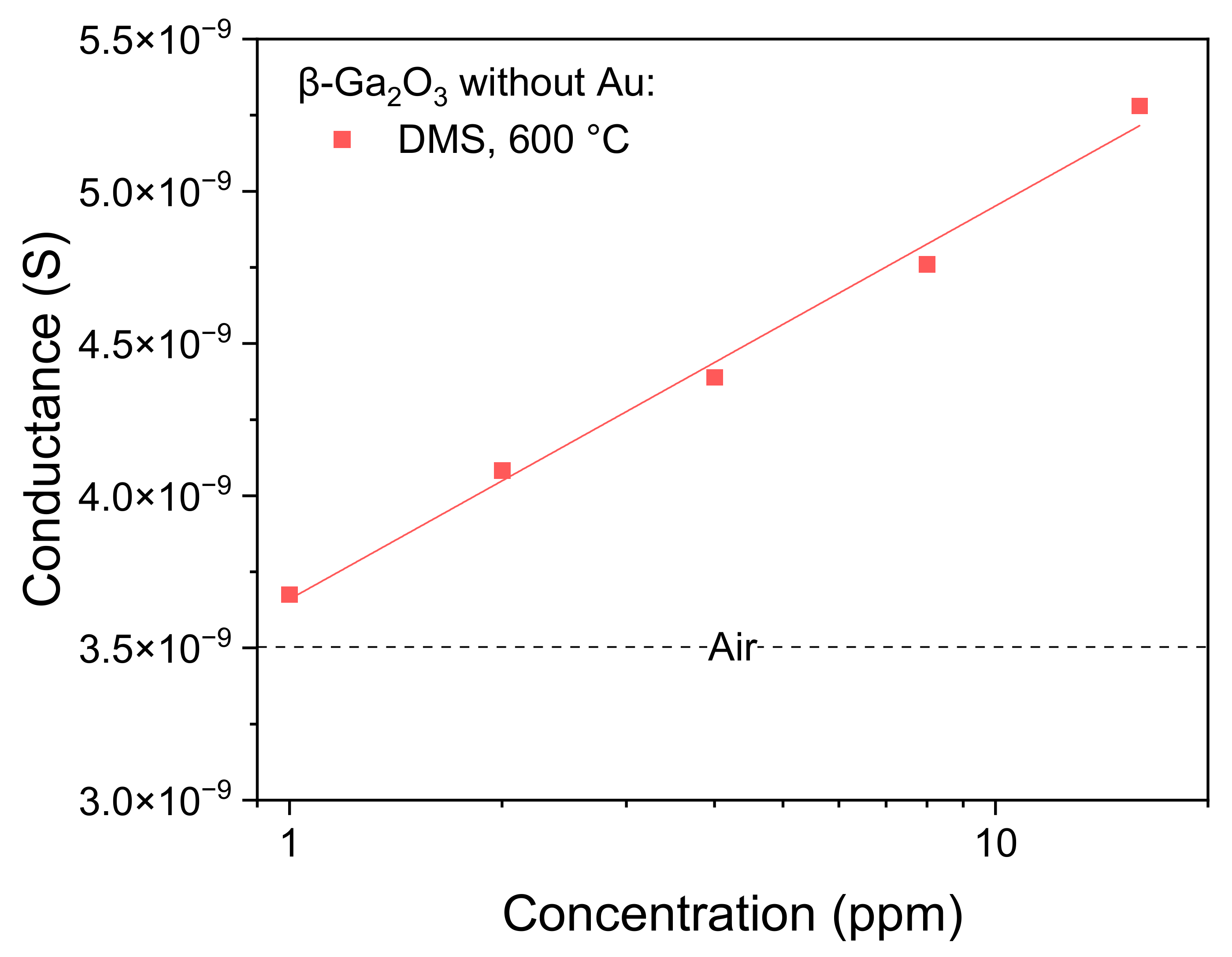
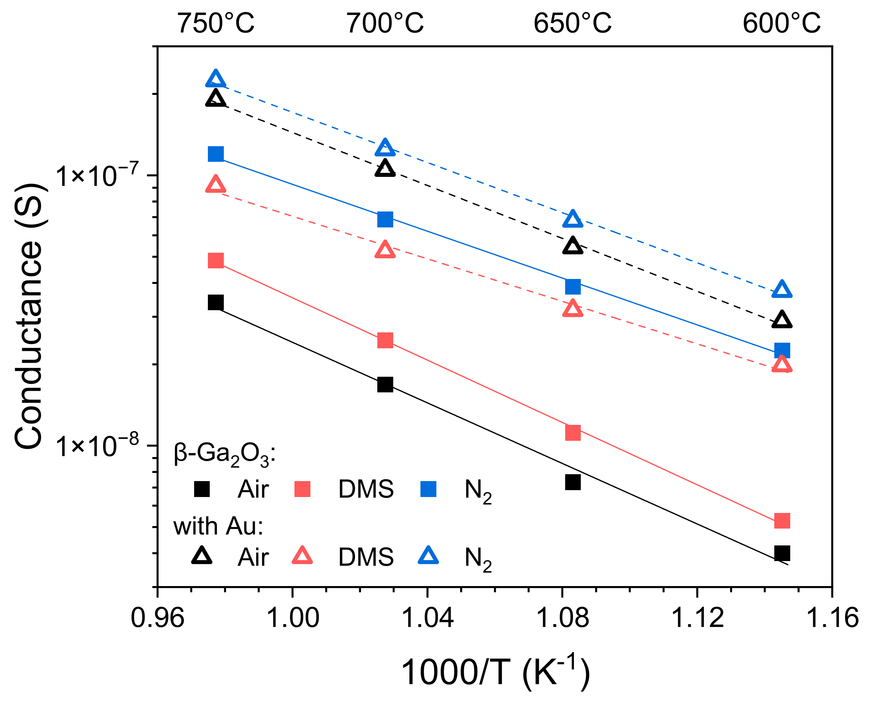
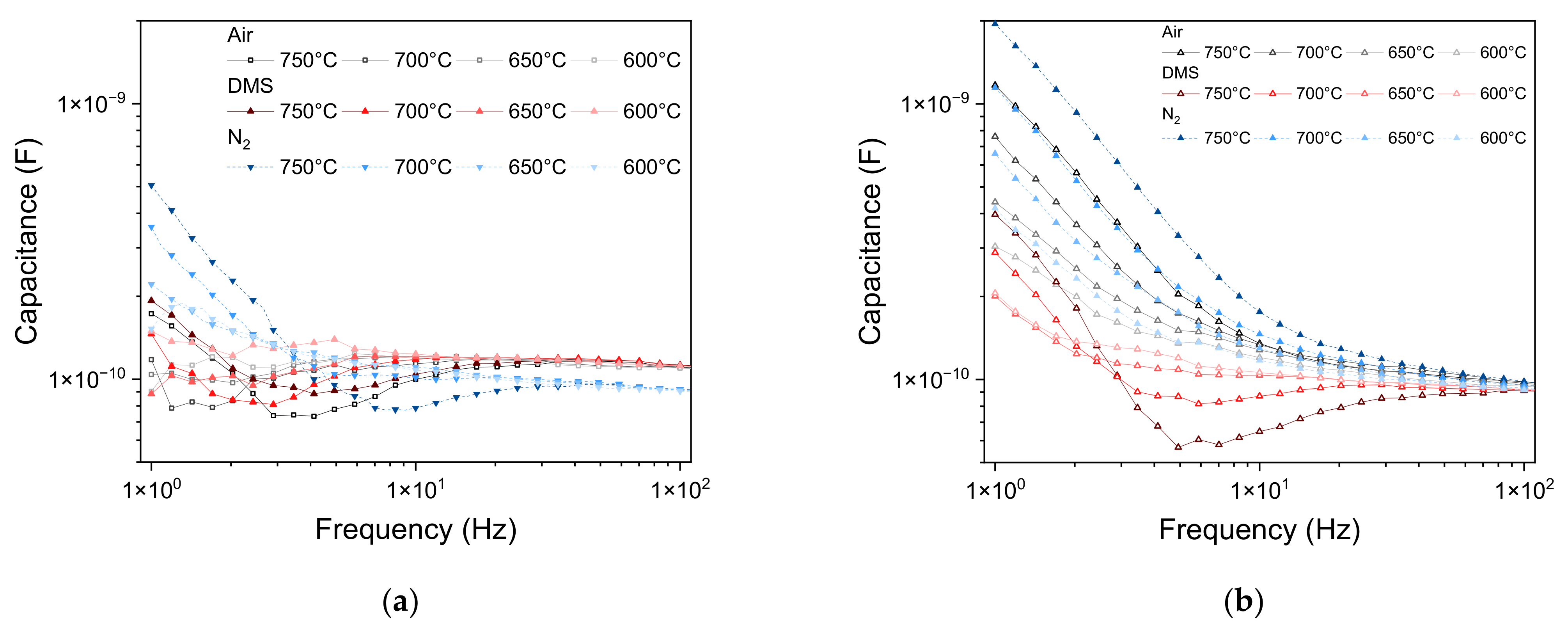
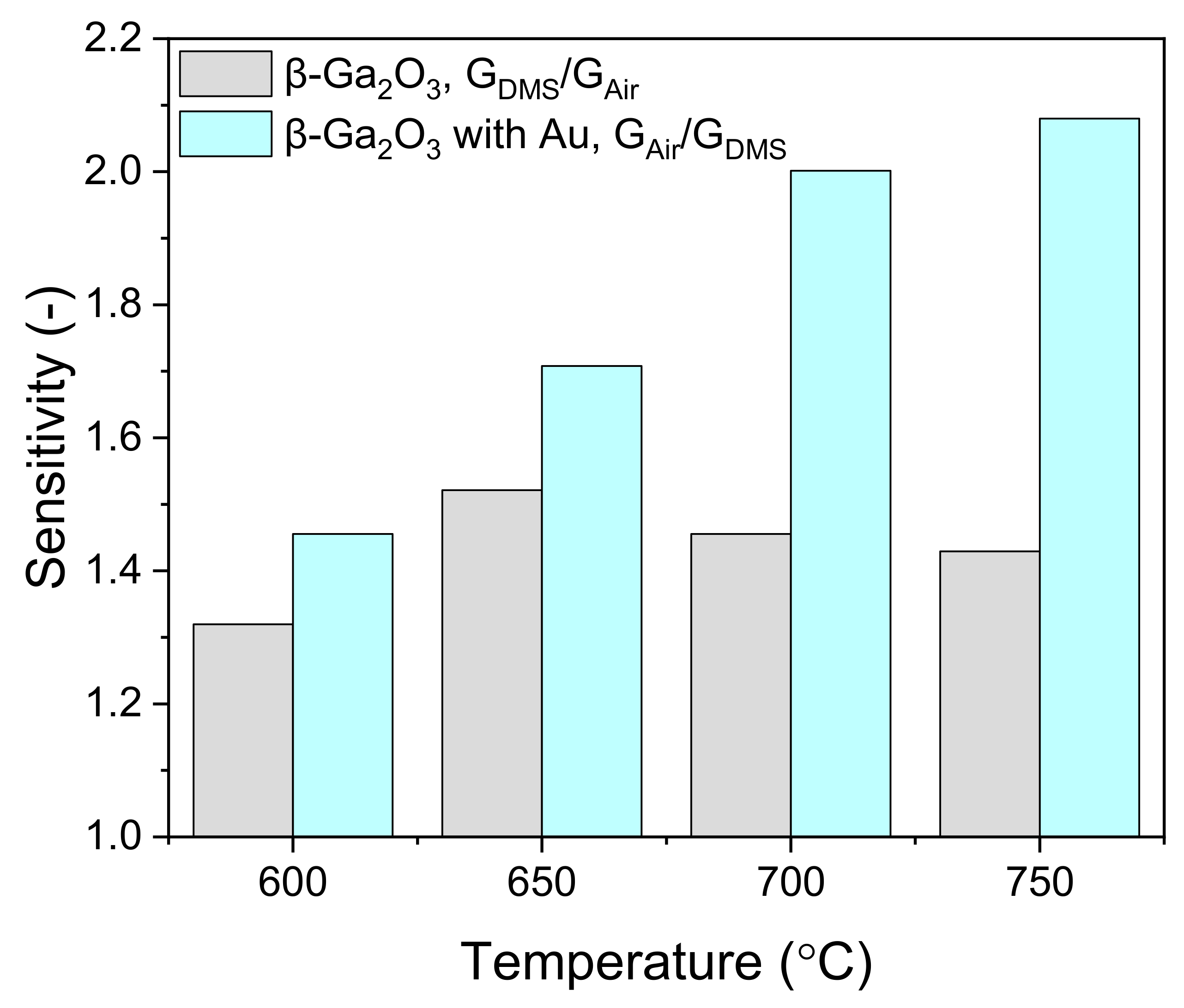
3.4. Impedance Spectroscopy
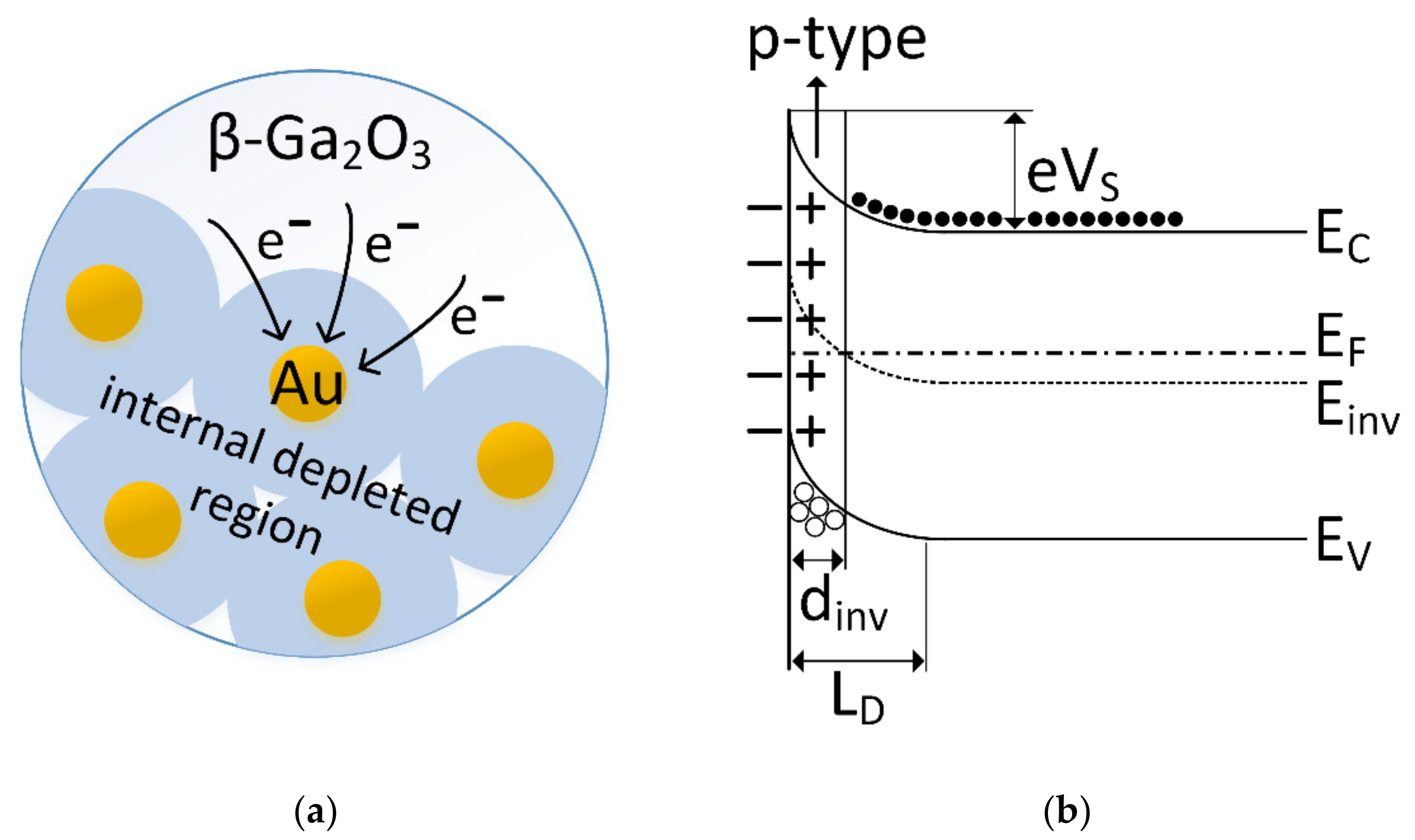
4. Discussion
5. Conclusions
Author Contributions
Funding
Institutional Review Board Statement
Informed Consent Statement
Data Availability Statement
Conflicts of Interest
References
- Kuramata, A.; Koshi, K.; Watanabe, S.; Yamaoka, Y.; Masui, T.; Yamakoshi, S. High-quality β-Ga2O3 single crystals grown by edge-defined film-fed growth. Jpn. J. Appl. Phys. 2016, 55, 1202A2. [Google Scholar] [CrossRef]
- Zhang, J.; Shi, J.; Qi, D.-C.; Chen, L.; Zhang, K.H.L. Recent progress on the electronic structure, defect, and doping properties of Ga2O3. APL Mater. 2020, 8, 020906. [Google Scholar] [CrossRef] [Green Version]
- Higashiwaki, M.; Sasaki, K.; Kuramata, A.; Masui, T.; Yamakoshi, S. Gallium oxide (Ga2O3) metal-semiconductor field-effect transistors on single-crystal β-Ga2O3 (010) substrates. Appl. Phys. Lett. 2012, 100, 013504. [Google Scholar] [CrossRef]
- Arora, K.; Kumar, M. Sputtered-Growth of High-Temperature Seed-Layer Assisted β-Ga2O3 Thin Film on Silicon-Substrate for Cost-Effective Solar-Blind Photodetector Application. ECS J. Solid State Sci. Technol. 2020, 9, 065013. [Google Scholar] [CrossRef]
- Shi, Y.-L.; Huang, D.; Ling, F.C.-C. Band offset and electrical properties of ErZO/β-Ga2O3 and GZO/β-Ga2O3 heterojunctions. Appl. Surf. Sci. 2022, 576, 151814. [Google Scholar] [CrossRef]
- Nakagomi, S.; Sai, T.; Kokubun, Y. Hydrogen gas sensor with self temperature compensation based on β-Ga2O3 thin film. Sens. Actuators B Chem. 2013, 187, 413–419. [Google Scholar] [CrossRef]
- Vorobyeva, N.; Rumyantseva, M.; Platonov, V.; Filatova, D.; Chizhov, A.; Marikutsa, A.; Bozhev, I.; Gaskov, A. Ga2O3(Sn) Oxides for High-Temperature Gas Sensors. Nanomaterials 2021, 11, 2938. [Google Scholar] [CrossRef] [PubMed]
- Patil, V.; Lee, B.-T.; Jeong, S.-H. Optical and structural characterization of high crystalline β-Ga2O3 films prepared using an RF magnetron sputtering. J. Alloys Compd. 2022, 894, 162551. [Google Scholar] [CrossRef]
- Murakami, H.; Nomura, K.; Goto, K.; Sasaki, K.; Kawara, K.; Thieu, Q.T.; Togashi, R.; Kumagai, Y.; Higashiwaki, M.; Kuramata, A.; et al. Homoepitaxial growth of β-Ga2O3 layers by halide vapor phase epitaxy. Appl. Phys. Express 2015, 8, 015503. [Google Scholar] [CrossRef]
- Boschi, F.; Bosi, M.; Berzina, T.; Buffagni, E.; Ferrari, C.; Fornari, R. Hetero-epitaxy of ε-Ga2O3 layers by MOCVD and ALD. J. Cryst. Growth 2016, 443, 25–30. [Google Scholar] [CrossRef]
- Nakagomi, S.; Kokubun, Y. Crystal orientation of β-Ga2O3 thin films formed on c-plane and a-plane sapphire substrate. J. Cryst. Growth 2012, 349, 12–18. [Google Scholar] [CrossRef]
- Shen, H.; Yin, Y.; Tian, K.; Baskaran, K.; Duan, L.; Zhao, X.; Tiwari, A. Growth and characterization of β-Ga2O3 thin films by sol-gel method for fast-response solar-blind ultraviolet photodetectors. J. Alloys Compd. 2018, 766, 601–608. [Google Scholar] [CrossRef]
- Kwon, O.S.; Hong, J.-Y.; Park, S.J.; Jang, Y.; Jang, J. Resistive Gas Sensors Based on Precisely Size-Controlled Polypyrrole Nanoparticles: Effects of Particle Size and Deposition Method. J. Phys. Chem. C 2010, 114, 18874–18879. [Google Scholar] [CrossRef]
- Korotcenkov, G. Current Trends in Nanomaterials for Metal Oxide-Based Conductometric Gas Sensors: Advantages and Limitations. Part 1: 1D and 2D Nanostructures. Nanomaterials 2020, 10, 1392. [Google Scholar] [CrossRef] [PubMed]
- Afzal, A. β-Ga2O3 nanowires and thin films for metal oxide semiconductor gas sensors: Sensing mechanisms and performance enhancement strategies. J. Mater. 2019, 5, 542–557. [Google Scholar] [CrossRef]
- Usseinov, A.; Koishybayeva, Z.; Platonenko, A.; Pankratov, V.; Suchikova, Y.; Akilbekov, A.; Zdorovets, M.; Purans, J.; Popov, A.I. Vacancy Defects in Ga2O3: First-Principles Calculations of Electronic Structure. Materials 2021, 14, 7384. [Google Scholar] [CrossRef] [PubMed]
- Kiss, G.; Krafcsik, O.H.; Kovács, K.; Josepovits, V.K.; Fleischer, M.; Meixner, H.; Deák, P.; Réti, F. Impedance spectroscopic and secondary ion mass spectrometric studies of β-Ga2O3/O2 interaction. Thin Solid Films 2001, 391, 239–242. [Google Scholar] [CrossRef]
- Bartic, M.; Baban, C.-I.; Suzuki, H.; Ogita, M.; Isai, M. β-Gallium Oxide as Oxygen Gas Sensors at a High Temperature. J. Am. Ceram. Soc. 2007, 90, 2879–2884. [Google Scholar] [CrossRef]
- Baban, C.; Toyoda, Y.; Ogita, M. Oxygen sensing at high temperatures using Ga2O3 films. Thin Solid Films 2005, 484, 369–373. [Google Scholar] [CrossRef]
- Almaev, A.V.; Chernikov, E.V.; Kushnarev, B.O.; Yakovlev, N.N. Effect of oxygen on the properties of Ga2O3:Si thin films. J. Phys. Conf. Ser. 2019, 1410, 012201. [Google Scholar] [CrossRef]
- Almaev, A.V.; Chernikov, E.V.; Novikov, V.V.; Kushnarev, B.O.; Yakovlev, N.N.; Chuprakova, E.V.; Oleinik, V.L.; Lozinskaya, A.D.; Gogova, D.S. Impact of Cr2O3 additives on the gas-sensitive properties of β-Ga2O3 thin films to oxygen, hydrogen, carbon monoxide, and toluene vapors. J. Vac. Sci. Technol. A 2021, 39, 023405. [Google Scholar] [CrossRef]
- Dyndal, K.; Zarzycki, A.; Andrysiewicz, W.; Grochala, D.; Marszalek, K.; Rydosz, A. CuO-Ga2O3 Thin Films as a Gas-Sensitive Material for Acetone Detection. Sensors 2020, 20, 3142. [Google Scholar] [CrossRef] [PubMed]
- Balasubramani, V.; Ahamed, A.N.; Chandraleka, S.; Kumar, K.K.; Kuppusamy, M.R.; Sridhar, T.M. Highly Sensitive and Selective H2S Gas Sensor Fabricated with β-Ga2O3/rGO. ECS J. Solid State Sci. Technol. 2020, 9, 055009. [Google Scholar] [CrossRef]
- Pandeeswari, R.; Jeyaprakash, B.G. High sensing response of β-Ga2O3 thin film towards ammonia vapours: Influencing factors at room temperature. Sens. Actuators B Chem. 2014, 195, 206–214. [Google Scholar] [CrossRef]
- Eastman, D.E. Photoelectric Work Functions of Transition, Rare-Earth, and Noble Metals. Phys. Rev. B 1970, 2, 1. [Google Scholar] [CrossRef]
- Michaelson, H.B. The work function of the elements and its periodicity. J. Appl. Phys. 1977, 48, 4729–4733. [Google Scholar] [CrossRef] [Green Version]
- Miao, Y.; Liang, B.; Tian, Y.; Xiong, T.; Sun, S.; Chen, C. Epitaxial growth of β-Ga2O3 nanowires from horizontal to obliquely upward evolution. Vacuum 2021, 192, 110444. [Google Scholar] [CrossRef]
- Jia, C.; Jeon, D.-W.; Xu, J.; Yi, X.; Park, J.-H.; Zhang, Y. Catalyst-Assisted Large-Area Growth of Single-Crystal β-Ga2O3 Nanowires on Sapphire Substrates by Metal–Organic Chemical Vapor Deposition. Nanomaterials 2020, 10, 1031. [Google Scholar] [CrossRef]
- Sivakumar, C.; Tsai, G.-H.; Chung, P.-F.; Balraj, B.; Lin, Y.-F.; Ho, M.-S. High-Quality Single-Crystalline β-Ga2O3 Nanowires: Synthesis to Nonvolatile Memory Applications. Nanomaterials 2021, 11, 2013. [Google Scholar] [CrossRef]
- Krawczyk, M.; Suchorska-Woźniak, P.; Szukiewicz, R.; Kuchowicz, M.; Korbutowicz, R.; Teterycz, H. Morphology of Ga2O3 Nanowires and Their Sensitivity to Volatile Organic Compounds. Nanomaterials 2021, 11, 456. [Google Scholar] [CrossRef] [PubMed]
- Lu, J.; Xing, J.; Chen, D.; Xu, H.; Han, X.; Li, D. Enhanced photocatalytic activity of β-Ga2O3 nanowires by Au nanoparticles decoration. J. Mater. Sci. 2019, 54, 6530–6541. [Google Scholar] [CrossRef]
- Zhang, H.; Deng, J.; Meng, T.; Xu, Z.; Li, R.; Sun, J.; Zhang, X.; Zhang, J.; Zhang, X. Growth of Au nanoparticles modified β-Ga2O3 film and enhanced performance in the photocatalytic decomposition. J. Mater. Sci. Mater. Electron. 2020, 31, 12522–12527. [Google Scholar] [CrossRef]
- Schwebel, T.; Fleischer, M.; Meixner, H.; Kohl, C.-D. CO-Sensor for domestic use based on high temperature stable Ga2O3 thin films. Sens. Actuators B Chem. 1998, 49, 46–51. [Google Scholar] [CrossRef]
- Feng, S.; Farha, F.; Li, Q.; Wan, Y.; Xu, Y.; Zhang, T.; Ning, H. Review on Smart Gas Sensing Technology. Sensors 2019, 19, 3760. [Google Scholar] [CrossRef] [PubMed] [Green Version]
- Wang, H.; Ma, J.; Zhang, J.; Feng, Y.; Vijjapu, M.T.; Yuvaraja, S.; Surya, S.G.; Salama, K.N.; Dong, C.; Wang, Y.; et al. Gas sensing materials roadmap. J. Phys. Condens. Matter 2021, 33, 303001. [Google Scholar] [CrossRef] [PubMed]
- Capone, S.; Forleo, A.; Francioso, L.; Rella, R.; Siciliano, P.; Spadavecchia, J.; Presicce, D.S.; Taurino, A.M. Solid state gas sensors: State of the art and future activities. J. Optoelectron. Adv. Mater. 2003, 5, 1335–1348. [Google Scholar] [CrossRef]
- Nikolaev, V.I.; Pechnikov, A.I.; Stepanov, S.I.; Nikitina, I.P.; Smirnov, A.N.; Chikiryaka, A.V.; Sharofidinov, S.S.; Bougrov, V.E.; Romanov, A.E. Epitaxial growth of (201) β-Ga2O3 on (0001) sapphire substrates by halide vapour phase epitaxy. Mater. Sci. Semicond. Process. 2016, 47, 16–19. [Google Scholar] [CrossRef]
- Suchorska-Woźniak, P.; Rac, O.; Klimkiewicz, R.; Fiedot, M.; Teterycz, H. Dehydrogenation properties of ZnO and the impact of gold nanoparticles on the process. Appl. Catal. A Gen. 2016, 514, 135–145. [Google Scholar] [CrossRef]
- Waseda, Y.; Matsubara, E.; Shinoda, K. X-ray Diffraction Crystallography; Springer: Berlin/Heidelberg, Germany, 2011; ISBN 978-3-642-16634-1. [Google Scholar]
- Zak, A.K.; Majid, W.A.; Abrishami, M.E.; Yousefi, R. X-ray analysis of ZnO nanoparticles by Williamson–Hall and size–strain plot methods. Solid State Sci. 2011, 13, 251–256. [Google Scholar] [CrossRef]
- Kushwaha, P.; Chauhan, P. Microstructural evaluation of iron oxide nanoparticles at different calcination temperature by Scherrer, Williamson-Hall, Size-Strain Plot and Halder-Wagner methods. Phase Transitions 2021, 94, 731–753. [Google Scholar] [CrossRef]
- Lasia, A. Electrochemical Impedance Spectroscopy and Its Applications; Springer: New York, NY, USA, 2014; ISBN 978-1-4614-8932-0. [Google Scholar]
- Schipani, F.; Miller, D.R.; Ponce, M.A.; Aldao, C.M.; Akbar, S.A.; Morris, P.A. Electrical Characterization of Semiconductor Oxide-Based Gas Sensors Using Impedance Spectroscopy: A Review. Rev. Adv. Sci. Eng. 2016, 5, 86–105. [Google Scholar] [CrossRef]
- Galazka, Z. β-Ga2O3 for wide-bandgap electronics and optoelectronics. Semicond. Sci. Technol. 2018, 33, 113001. [Google Scholar] [CrossRef]
- Wei, Z.; Akbari, M.K.; Hai, Z.; Ramachandran, R.K.; Detavernier, C.; Verpoort, F.; Kats, E.; Xu, H.; Hu, J.; Zhuiykov, S. Ultra-thin sub-10 nm Ga2O3-WO3 heterostructures developed by atomic layer deposition for sensitive and selective C2H5OH detection on ppm level. Sens. Actuators B Chem. 2019, 287, 147–156. [Google Scholar] [CrossRef]
- Demin, I.E.; Kozlov, A.G. In2O3–Ga2O3 thin films for ammonia sensors of petrochemical industry safety systems.; 2018; p. 050004. In AIP Conference Proceedings; AIP Publishing LLC: Melville, NY, USA.
- Wang, Y.; Duan, L.; Deng, Z.; Liao, J. Electrically Transduced Gas Sensors Based on Semiconducting Metal Oxide Nanowires. Sensors 2020, 20, 6781. [Google Scholar] [CrossRef]
- Teterycz, H.; Halek, P.; Wiśniewski, K.; Halek, G.; Koźlecki, T.; Polowczyk, I. Oxidation of Hydrocarbons on the Surface of Tin Dioxide Chemical Sensors. Sensors 2011, 11, 4425–4437. [Google Scholar] [CrossRef] [PubMed]
- Fleischer, M.; Meixner, H. Selectivity in high-temperature operated semiconductor gas-sensors. Sens. Actuators B Chem. 1998, 52, 179–187. [Google Scholar] [CrossRef]
- Xu, C.; Tamaki, J.; Miura, N.; Yamazoe, N. Grain size effects on gas sensitivity of porous SnO2-based elements. Sens. Actuators B Chem. 1991, 3, 147–155. [Google Scholar] [CrossRef]
- Sze, S.M.; Ng, K.K. Physics of Semiconductor Devices; John Wiley & Sons, Inc.: Hoboken, NJ, USA, 2006; ISBN 9780470068328. [Google Scholar]
- Stoneham, A. Oxide Surfaces: The Basic Processes of Sensor Behaviour in Solid State Gas Sensors; Hilger, A., Ed.; Adam Hilger: Bristol, UK, 1987. [Google Scholar]
- Nenov, T.G.; Yordanov, S.P. Ceramic Sensors; CRC Press: Boca Raton, FL, USA, 2020; ISBN 9781003075837. [Google Scholar]
- Meyer, R.; Lemire, C.; Shaikhutdinov, S.K.; Freund, H.-J. Surface chemistry of catalysis by gold. Gold Bull. 2004, 37, 72–124. [Google Scholar] [CrossRef] [Green Version]
- Janssens, T.V.W.; Clausen, B.S.; Hvolbæk, B.; Falsig, H.; Christensen, C.H.; Bligaard, T.; Nørskov, J.K. Insights into the reactivity of supported Au nanoparticles: Combining theory and experiments. Top. Catal. 2007, 44, 15–26. [Google Scholar] [CrossRef]
- Canning, N.D.S.; Outka, D.; Madix, R.J. The adsorption of oxygen on gold. Surf. Sci. 1984, 141, 240–254. [Google Scholar] [CrossRef]
- Outka, D.A.; Madix, R.J. The oxidation of carbon monoxide on the Au(110) surface. Surf. Sci. 1987, 179, 351–360. [Google Scholar] [CrossRef]
- Gottfried, J.; Elghobashi, N.; Schroeder, S.L.; Christmann, K. Oxidation of gold by oxygen-ion sputtering. Surf. Sci. 2003, 523, 89–102. [Google Scholar] [CrossRef]
- Gines, M.J.L.; Iglesia, E. Bifunctional Condensation Reactions of Alcohols on Basic Oxides Modified by Copper and Potassium. J. Catal. 1998, 176, 155–172. [Google Scholar] [CrossRef] [Green Version]
- Flores, F.; Miranda, R. Tuning Schottky Barriers by atomic layer control at metal-semiconductor interfaces. Adv. Mater. 1994, 6, 540–548. [Google Scholar] [CrossRef]
- Sun, L.; Zhao, D.; Song, Z.; Shan, C.; Zhang, Z.; Li, B.; Shen, D. Gold nanoparticles modified ZnO nanorods with improved photocatalytic activity. J. Colloid Interface Sci. 2011, 363, 175–181. [Google Scholar] [CrossRef] [PubMed]
- Licznerski, B.; Nitsch, K.; Teterycz, H.; Wiśniewski, K. The influence of Rh surface doping on anomalous properties of thick-film SnO2 gas sensors. Sens. Actuators B Chem. 2001, 79, 157–162. [Google Scholar] [CrossRef]
- Teterycz, H.; Licznerski, B.; Nitsch, K.; Wiśniewski, K.; Golonka, L. Anomalous behaviour of new thick film gas sensitive composition. Sens. Actuators B Chem. 1998, 47, 153–157. [Google Scholar] [CrossRef]
- Pliskin, W.A. Comparison of properties of dielectric films deposited by various methods. J. Vac. Sci. Technol. 1977, 14, 1064–1081. [Google Scholar] [CrossRef]
- Zhong, H.; Heuss, G.; Misra, V. Electrical properties of RuO2 gate electrodes for dual metal gate Si-CMOS. IEEE Electron Device Lett. 2000, 21, 593–595. [Google Scholar] [CrossRef]
- Passlack, M.; Schubert, E.F.; Hobson, W.S.; Hong, M.; Moriya, N.; Chu, S.N.G.; Konstadinidis, K.; Mannaerts, J.P.; Schnoes, M.L.; Zydzik, G.J. Ga2O3 films for electronic and optoelectronic applications. J. Appl. Phys. 1995, 77, 686–693. [Google Scholar] [CrossRef]
- Lee, S.-A.; Hwang, J.-Y.; Kim, J.-P.; Jeong, S.-Y.; Cho, C.-R. Dielectric characterization of transparent epitaxial Ga2O3 thin film on n-GaN∕Al2O3 prepared by pulsed laser deposition. Appl. Phys. Lett. 2006, 89, 182906. [Google Scholar] [CrossRef]
- Irmscher, K.; Galazka, Z.; Pietsch, M.; Uecker, R.; Fornari, R. Electrical properties of β-Ga2O3 single crystals grown by the Czochralski method. J. Appl. Phys. 2011, 110, 063720. [Google Scholar] [CrossRef]
- Kokkin, D.L.; Zhang, R.; Steimle, T.C.; Wyse, I.A.; Pearlman, B.W.; Varberg, T.D. Au–S Bonding Revealed from the Characterization of Diatomic Gold Sulfide, AuS. J. Phys. Chem. A 2015, 119, 11659–11667. [Google Scholar] [CrossRef] [PubMed]
- Srinivasan, P.; Rayappan, J.B.B. Investigations on room temperature dual sensitization of ZnO nanostructures towards fish quality biomarkers. Sens. Actuators B Chem. 2020, 304, 127082. [Google Scholar] [CrossRef]


| Oxygen Bonds | Unmodified β-Ga2O3 | β-Ga2O3 Impregnated with Au Nanoparticles |
|---|---|---|
| Ga-O | 5.68% | 4.61% |
| O-C, O=C | 19.30% | 17.48% |
| OH- | 1.94% | 4.54% |
| Atmosphere Composition | Unmodified β-Ga2O3 | β-Ga2O3 Impregnated with Au Nanoparticles |
|---|---|---|
| Ambient air | (1.11 ± 0.07) eV | (0.97 ± 0.03) eV |
| Dry nitrogen | (0.86 ± 0.03) eV | (0.92 ± 0.03) eV |
| Ambient air + 16 ppm dimethyl sulfide | (1.14 ± 0.03) eV | (0.78 ± 0.05) eV |
Publisher’s Note: MDPI stays neutral with regard to jurisdictional claims in published maps and institutional affiliations. |
© 2022 by the authors. Licensee MDPI, Basel, Switzerland. This article is an open access article distributed under the terms and conditions of the Creative Commons Attribution (CC BY) license (https://creativecommons.org/licenses/by/4.0/).
Share and Cite
Krawczyk, M.; Korbutowicz, R.; Szukiewicz, R.; Suchorska-Woźniak, P.; Kuchowicz, M.; Teterycz, H. P-type Inversion at the Surface of β-Ga2O3 Epitaxial Layer Modified with Au Nanoparticles. Sensors 2022, 22, 932. https://0-doi-org.brum.beds.ac.uk/10.3390/s22030932
Krawczyk M, Korbutowicz R, Szukiewicz R, Suchorska-Woźniak P, Kuchowicz M, Teterycz H. P-type Inversion at the Surface of β-Ga2O3 Epitaxial Layer Modified with Au Nanoparticles. Sensors. 2022; 22(3):932. https://0-doi-org.brum.beds.ac.uk/10.3390/s22030932
Chicago/Turabian StyleKrawczyk, Maciej, Ryszard Korbutowicz, Rafał Szukiewicz, Patrycja Suchorska-Woźniak, Maciej Kuchowicz, and Helena Teterycz. 2022. "P-type Inversion at the Surface of β-Ga2O3 Epitaxial Layer Modified with Au Nanoparticles" Sensors 22, no. 3: 932. https://0-doi-org.brum.beds.ac.uk/10.3390/s22030932