Article

PLL-Based Readout Circuit for SiC-MOS Capacitor Hydrogen Sensors in Industrial Environments

1
Faculty of Electronics, Telecommunications and Information Technology, University Politehnica of Bucharest, 061071 Bucharest, Romania
2
National Institute for Research and Development in Microtechnologies (IMT), 077190 Voluntari, Romania
3
Romanian Young Academy, Research Institute of the University of Bucharest, University of Bucharest, 030018 Bucharest, Romania
*
Authors to whom correspondence should be addressed.
Submission received: 29 December 2021 / Revised: 19 January 2022 / Accepted: 9 February 2022 / Published: 14 February 2022
(This article belongs to the Special Issue Hazardous Gas Sensing for Environment Safety)

Abstract

:
For proper operation in real industrial conditions, gas sensors require readout circuits which offer accuracy, noise robustness, energy efficiency and portability. We present an innovative, dedicated readout circuit with a phase locked loop (PLL) architecture for SiC-MOS capacitor sensors. A hydrogen detection system using this circuit is designed, simulated, implemented and tested. The PLL converts the MOS nonlinear small-signal capacitance (affected by hydrogen) into an output voltage proportional to the detected gas concentration. Thus, the MOS sensing element is part of the PLL’s voltage-controlled oscillator. This block effectively provides a small AC signal (around 70 mV at 1 MHz) for the sensor and acquires its response. The correct operation of the proposed readout circuit is validated by simulations and experiments. Hydrogen measurements are performed for concentrations up to 1600 ppm. The PLL output exhibited voltage variations close to those discernable from experimental C-V curves, acquired with a semiconductor characterization system, for all investigated MOS sensor samples.

1. Introduction

The applications of gas sensors have broadened considerably over time, extending from monitoring concentrations under the olfactory human limit to detecting the presence of dangerous compounds and ensuring work safety. Notably, volatile organic compounds (VOCs), H2S and NO2 are among the substances of interest when checking whether an environment is habitable or work suitable. In industry, the monitoring of flammable or explosive gases has become essential for guaranteeing fast responses to leaks and avoiding casualties/infrastructure damage [1]. In the search for clean and renewable energy, hydrogen (H2) has emerged as one of the leading candidates [2,3,4,5,6,7,8,9,10]. However, it is a highly explosive gas, if its concentration in air exceeds 4.65% [11,12]. Therefore, the need for high performance sensors (and associated readout circuits) to detect H2 in multiple applications is increasing rapidly [13]. Oftentimes, these applications are in harsh environments, such as the aerospace domain [11,14,15] the industrial sector [16,17] or, more recently, the automotive field for hydrogen powered vehicles [18,19].
Among detectors with various transduction mechanisms, gas sensors with capacitive components, such as metal-oxide-semiconductor (MOS) capacitors, interdigitated electrode (IDE) capacitors and quartz crystal microbalances (QCM) resonators are preferable due to their size, low cost and sensitivity [20]. MOS structures, in particular, can be fabricated using simple, well-established technological processes and, as opposed to their IDE and QCM counterparts, they do not require special coatings for compound detection [20]. Additionally, their capacitance can also be voltage-controlled, which gives flexibility in tuning a sensor’s baseline output (in an inert atmosphere). Although their optimal operation usually requires heating, this aspect is lower for industrial applications where the various processes that demand gas monitoring also entail elevated temperatures. For such hostile environments, silicon carbide (SiC) H2 MOS capacitor sensors are a suitable variant [16,20,21,22,23,24,25]. These sensors have been shown to be able to operate at high temperatures [16,20] up to 500 °C [16]. They also exhibit short response and recovery times [20] and good sensitivity to even small concentrations of H2 (as low as 20 ppm [22]). This optimal behavior is achieved with the MOS capacitor biased in the region where the capacitance is strongly dependent on applied voltage. In most prior studies [16,20,21,22,23,24,25] these performances were measured under laboratory conditions, with the sensor small-signal C-V characteristics extracted using semiconductor parameter analyzers. In order to ensure precision, noise suppression, energy efficiency and portability requirements for sensor operation in real conditions, a readout circuit is mandatory [26,27,28,29,30]. However, contributions pertaining to such circuit architectures suitable for SiC-MOS capacitor hydrogen sensors are scarce [30].
The topology described in [30] used a quad-diode bridge circuit with the MOS capacitor sensor connected as the bridge load. In this architecture, a variation in the active sensor capacitance led to a shift in the common mode DC voltage at the bridge input.
This paper proposes a portable hydrogen detection system with alternate readout circuit architecture. The sensing element is a SiC-MOS capacitor. The innovative readout circuit is essentially a phase locked loop (PLL) [31,32,33,34].
Readout circuits with PLLs have been previously used for gas sensing [35,36,37]. In these applications, the effective PLL block performs modulation/demodulation, enabling accurate frequency sweeping (necessary for sensing with high specificity and sensitivity). The main drawback is the high operating frequency (over 200 GHz), requiring implementation in advanced SiGe processes [35,36,37].
For our work, the PLL readout circuit was used as a capacitance to voltage converter, at a relatively low operating frequency (1 MHz). Its purpose was to reproduce the measurement conditions given by the parameter analyzer, but in a cost-effective form (for use in industrial applications). As the sensor was exposed to hydrogen, its C-V characteristic shifted [22] and the PLL varied the bias to maintain a constant capacitance, thus generating a voltage value proportional to the H2 concentration. Moreover, the PLL topology allowed for selecting the initial sensor bias voltage (i.e., at 0 ppm H2) to achieve optimal sensitivity [33]. Unlike conventional readout circuit architectures [30] it does not require dedicated bias and amplification blocks.
Section 2 describes the technological process flows for the SiC-MOS capacitor sensor, the structure of the PLL architecture and constituent blocks’ design. Section 3 presents simulation and experimental results demonstrating the correct operation of the proposed PLL topology. H2 measurements were carried out to validate the functionality of the complete hydrogen detection system.

2. Materials and Methods

The proposed system comprises two main parts: a SiC-MOS capacitor hydrogen sensor and a PLL-based readout circuit, designed for implementation with discrete components. The system generates an output voltage proportional to the hydrogen concentration detected by the sensor.

2.1. Hydrogen Sensor Structure

The SiC-MOS capacitors were fabricated starting from a 4H-SiC wafer with epitaxial layer. The doping concentration of the epi layer is around 2 × 1016 cm−3, while the substrate is heavily doped (−1018 cm−3).
A top view image of the structure is depicted in Figure 1. A 1 µm thick field oxide was deposited through low pressure chemical vapor deposition on the front side of the SiC surface. The active areas (400 µm diameter circular windows) were defined by etching with a ramp oxide profile [20]. The MOS oxide (SiO2) was grown in a dry oxygen atmosphere at a temperature of 1100 °C for 4 h, resulting in a thickness of 33 nm. After the oxidation process, a rapid postoxidation annealing was performed in a N2 atmosphere, at 1100 °C for 6 min. This treatment was demonstrated to both diminish the interface states density and improve the performance of the MOS device as hydrogen sensor [22]. Subsequently, a layer of Pd (50 nm) was deposited and defined on the window (Figure 1). Pd is a well-known catalytic metal with high hydrogen solubility [16]. The backside ohmic contact and the front side pads were formed by a successive deposition of Cr (15 nm)/Au (100 nm). The final devices were diced into chips and encapsulated in TO 39 packages using wire bonding technology.
The supplementary contact pad shown in Figure 1 is a “dummy” structure used for parasitic capacitance evaluation [20].

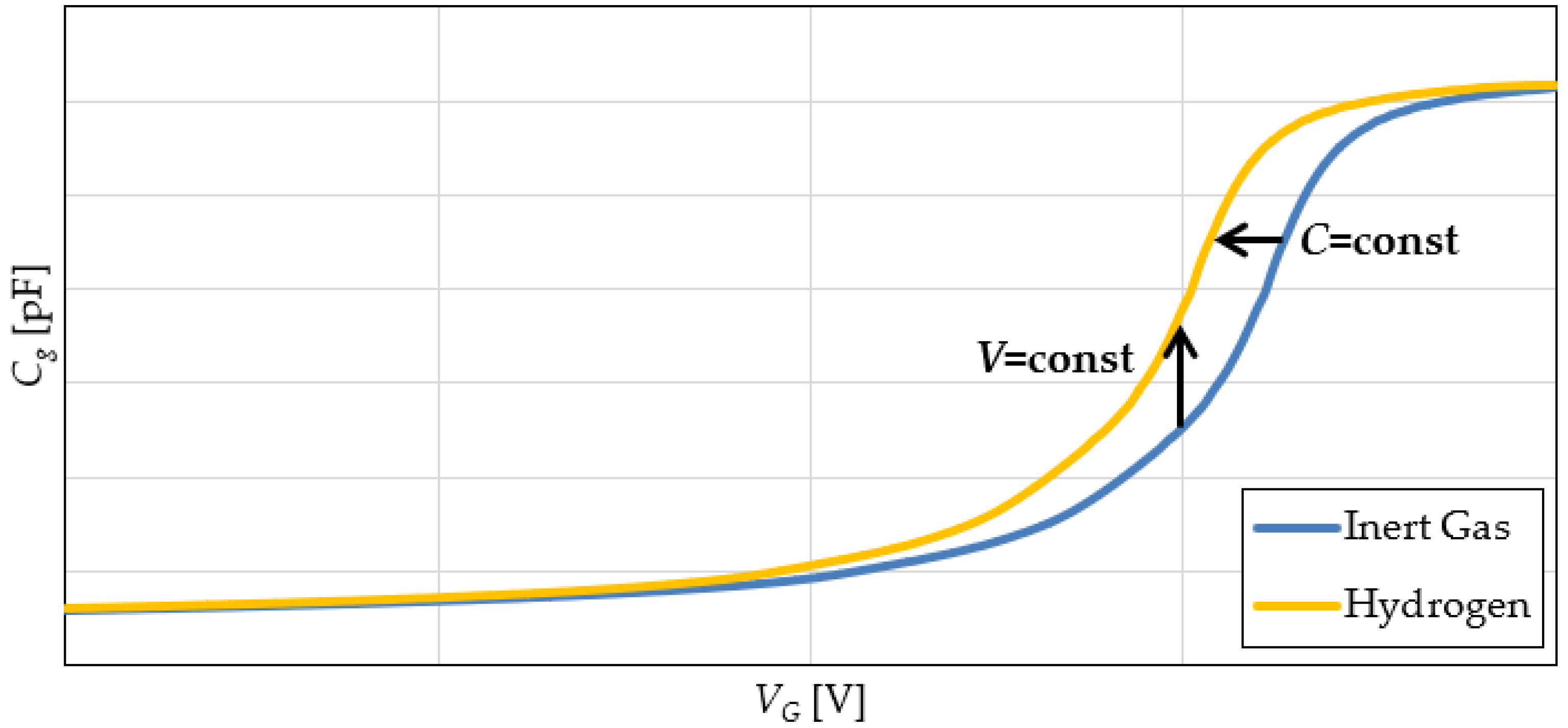
2.2. Hydrogen Detection Principle

Several interactions between hydrogen and our SiC-MOS structures were responsible for the overall sensing mechanism [22]. First, as molecular H2 was adsorbed at the active sensor area, it was dissociated into atomic form H+ at the Pd/SiO2 interface. As such, the Pd work function chemically shifted. Cumulatively with this effect, charged states presented at the metal-oxide interface were also passivated, creating a dipole layer between Pd and SiO2. However, it was shown that the main contributor to hydrogen sensitivity was given by the further diffusion of H+ deeper into the oxide and interaction with SiO2 bulk traps [22,38,39,40]. The trade-offs for this increase in susceptibility to H2 were that the structure took a longer time to both stabilize its response and to release stored hydrogen atoms as the environment becomes inert.
The characteristic of interest for the MOS capacitor sensor was the small-signal capacitance, denoted by Cg, versus the DC bias voltage, VG (C-V characteristic), measured at a frequency of 1 MHz. Two theoretical C-V curves (in an inert gas and in the presence of H2) are given in Figure 2 [22,33]. It can be seen that the presence of H2 leads to a left shift of the C-V characteristic [22]. This behavior is most obvious in the region where the capacitance is strongly dependent on the bias voltage. As a result, two hydrogen detection principles may be used, illustrated in Figure 2 [33].
Principle V = const implies maintaining a constant bias voltage across the MOS sensor and allowing its capacitance to vary. The most simple transducer in this scenario could be an oscillator which includes the capacitive sensor. Thus, the output quantity would be the oscillator frequency, which would change as the small-signal capacitance varies.
The C = const technique involves a constant sensor capacitance, which must be maintained by adjusting the DC bias voltage. In this case, the sensor can again be included in an oscillator, with a carefully chosen structure to allow for sensor bias control. This voltage controlled oscillator (VCO) will then be integrated into a phase locked loop (PLL) [31,32]. The PLL will adjust the bias voltage in order to maintain a constant VCO frequency (and thus sensor capacitance). The output quantity in this case is the sensor bias voltage. It is also the PLL error voltage [31,32].
In our implementation, the C = const approach is proposed for two reasons:
  • The frequency of the small signal applied to the sensor is constant and can be made equal to the characterization frequency. This is preferable because the sensor capacitance also depends on frequency, and frequency shifts may affect precision;
  • In a portable circuit solution, it is easier to process a constant voltage output than a frequency output.

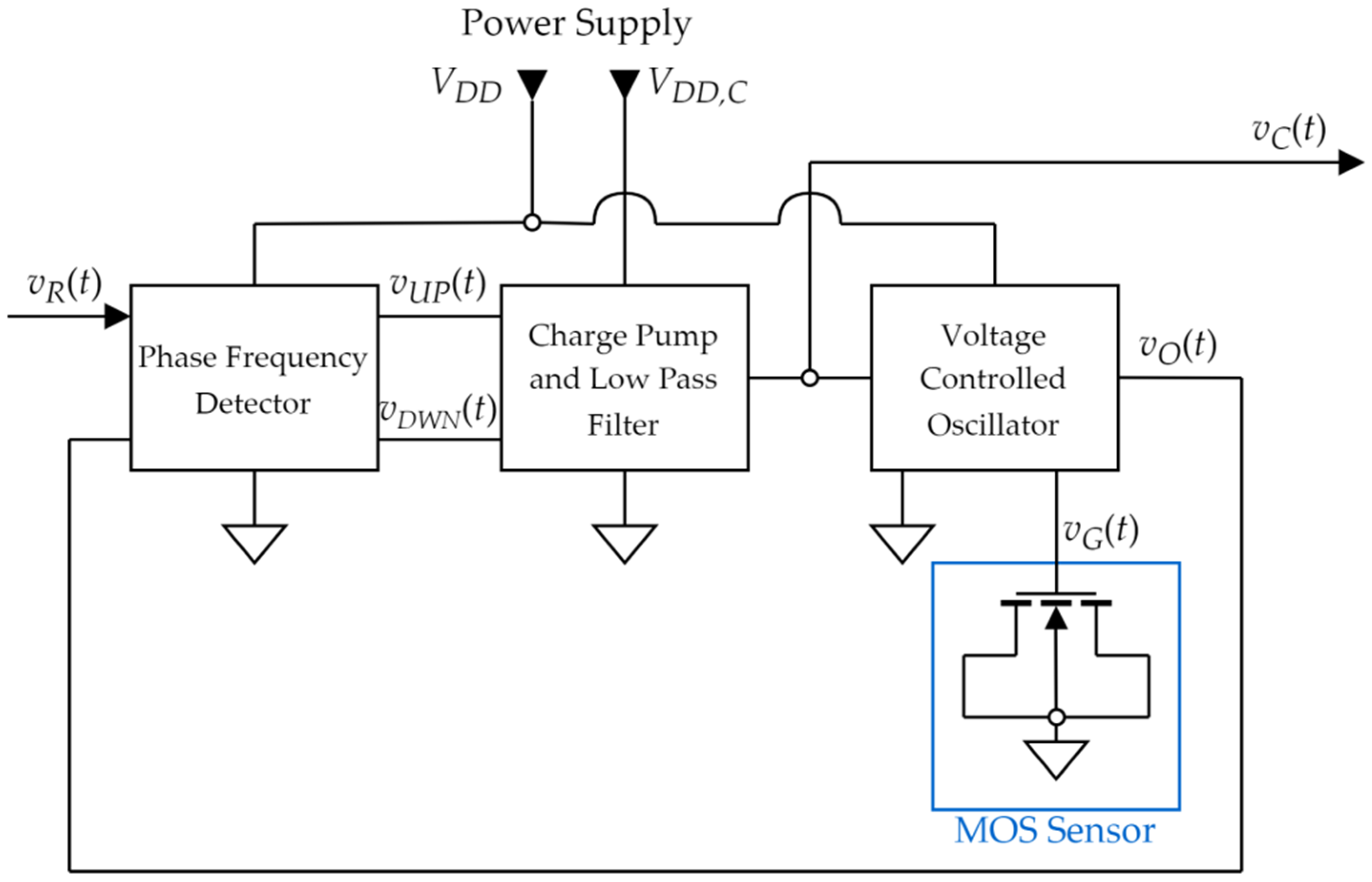
2.3. Readout Circuit

2.3.1. Phase Locked Loop

The proposed readout circuit is a digital phase locked loop (PLL) structure [31] intended to operate at a frequency of 1 MHz (the characterization frequency of the sensor). Its block schematic is shown in Figure 3.
The readout circuit architecture in Figure 3 has three main blocks:
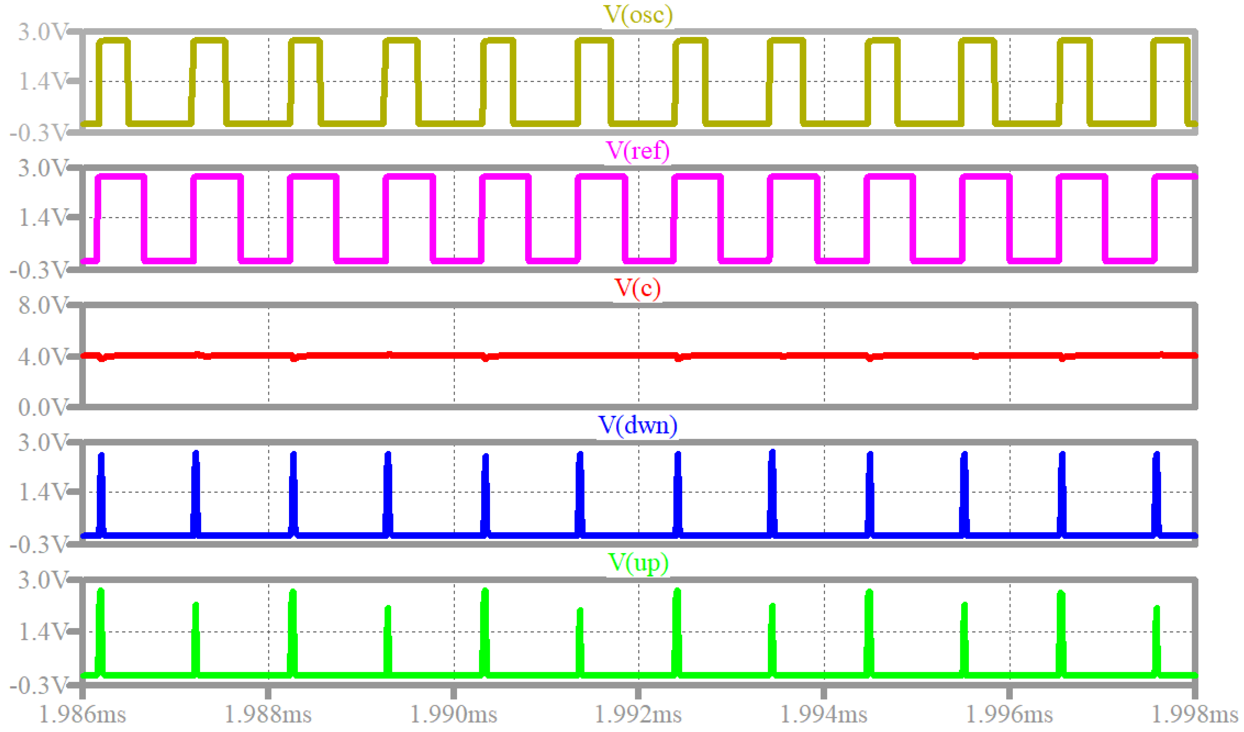
  • A voltage controlled oscillator (VCO) [33,34] generates an output periodic wave vO(t) with a frequency determined by the control voltage vC(t). It also applies a voltage vG(t) across the sensor, with a DC component (roughly equal to vC(t)) and an AC component. It is critical for accurate H2 measurement that the AC component be a small signal (<100 mV peak-to-peak).
  • A phase frequency detector (PFD) acquires the phase shift between VCO output vO(t) and a reference input signal vR(t), resulting from their frequency imbalance. It generates pulsed UP and DOWN signals (vUP(t), vDWN(t) Figure 3) with variable duty cycles, indicating whether the control voltage should be increased or decreased;
  • A charge pump (CP) and low pass filter (LPF) generate the control voltage based on the duty cycle difference between the UP and DOWN signals. The LPF uses an active inverting structure and has a key role in ensuring PLL stability [31].
  • The proposed PLL structure requires two supply voltages:
  • VDD—low voltage supply—for powering the oscillator and the low voltage logic in the phase frequency detector;
  • VDD,C—high voltage supply—for powering the charge pump and active low-pass filter.
In brief, the intended operation of the PLL is based on negative feedback: when the gas concentration increases, MOS sensor capacitance will tend to increase (see Figure 2). This leads to a decrease in the frequency of vO(t) (Figure 3), becoming lower than the frequency of vR(t). The PFD will detect this and set the UP signal to a duty cycle higher than that of the DOWN signal. Therefore, the UP command becomes dominant, and the CP and LPF blocks will decrease the control voltage vc(t). As a result, the bias voltage of the MOS gas sensor is decreased, thus also lowering the capacitance. In this manner, the PLL maintains a VCO frequency equal to the reference frequency, with the consequence being that the sensor capacitance is also kept constant (as per principle C = const from Figure 2). The output of the entire sensing ensemble is considered to be the oscillator control voltage (vC(t), Figure 3).
The supply voltages have separate filters for each of the blocks (and sometimes for individual elements of the same block, such as for the CP and the LPF). These filters are designed to ensure at least a 40 dB noise reduction from the supply of one block to the supply of another at the intended operating frequency of 1 MHz.

2.3.2. Voltage Controlled Oscillator

The proposed VCO was developed starting from the Armstrong architecture [41] and is shown in Figure 4 [33].
In the schematic from Figure 4, the bipolar transistor Q is the amplifying element [33]. Its quiescent point is set through resistors R1 and R2. The positive feedback loop is created through the coupled inductors L1 and L2. The theoretical oscillation frequency is given by [33]:
f o s c = 1 2 π L 2 [ C 1 ( C 3 + C g ) C 1 + C 3 + C g + C 2 C IN C 2 + C IN ]
where Cg is the sensor capacitance, C3 is used to trim the oscillation frequency and CIN is the input capacitance of the transistor. C1 and C2 are decoupling capacitors, which should have little effect on fosc due to their large capacitance. They are needed to separate the DC bias circuit of the transistor, the L2 inductor (DC voltage is 0) and the sensor voltage (DC voltage equal to vC(t)). For correct decoupling, C1 and C2 should be selected to be at least an order of magnitude larger than either CIN or C3 + Cg. Under these conditions, the oscillation frequency can be approximated as:
f osc = 1 2 π L 2 ( C 3 + C g + C IN )
CIN is given by
C IN = C π + C μ ( 1 + | A v | )
In which Av is the voltage gain of the amplifier formed with Q, R1 and R2.
For high system sensitivity, Cg should be dominant in establishing the oscillation frequency of the VCO. If CIN is too large, the influence of the sensor capacitance on the oscillation frequency is reduced and detecting small changes in gas concentration becomes difficult. On the other hand, Av should be large enough to ensure sufficient output (vO(t), Figure 4) amplitude, despite the small signal conditions present at the input. As such, Expressions (2) and (3) suggest a critical requirement for the bipolar transistor: internal capacitances (Cπ and Cµ) as low as possible.
RS (Figure 4) is a separation resistor which allows the sensor voltage vG(t) to have both a DC and a small signal AC component. Its presence is required since, when the PLL is locked, vC(t) is a purely DC signal provided by the LPF. For correct operation of the PLL, the RS resistance should be significantly lower than the parasitic parallel resistance of the MOS capacitor sensor but high enough to ensure correct separation. Furthermore, stability must also be taken into account when selecting RS, since it contributes to determining the loop bandwidth. This is because, as seen in Figure 4, RS, C3 and Cg form another low-pass filter (in addition to the block illustrated in Figure 3).
The oscillator is designed to achieve the target frequency of 1 MHz (trimmable via C3. Figure 4) at a control voltage vC(t) of around 4 V [33]. A small signal level (<100 mV) at the sensor node (vG(t)) is also targeted. Given the previous considerations and the design targets, the VCO component types and values from Table 1 are chosen [33].
The main advantage of this topology is that the sensor is biased with a DC voltage referred to ground. This allows for simpler control circuitry (charge pump, CP, and low-pass filter, LPF), since it only needs to generate one bias voltage. Moreover, the output voltage of the PLL (i.e., the voltage across the sensor) is also referred to ground, which simplifies the measurement. For instance, in a topology where the MOS sensor substrate is not connected to a ground, its body potential could change due to supply voltage variations, temperature, etc. Thus, it cannot be considered a constant reference and would have to be resampled for every individual measurement. Furthermore, in such a topology, the measurement could be further complicated by the fact that the substrate potential also has an AC component. Therefore, the Armstrong architecture, with the sensor body at ground, is more suitable for the proposed PLL measurement system.
Another important advantage of the Armstrong topology in Figure 4 is that, if properly designed, it allows the MOS capacitor to operate at small signal levels (<100 mV peak-to-peak). This is essential for linear operation of the sensor and thus for precise measurements.

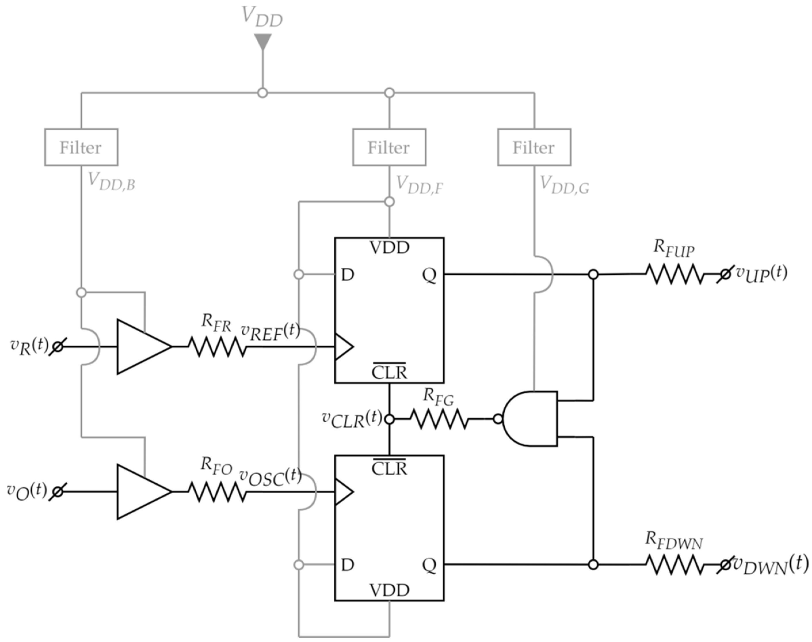
2.3.3. Phase Frequency Detector

The phase frequency detector, based on a well-known digital architecture [31,44] has the schematic shown in Figure 5. The advantage of this topology versus more simple detectors (such as a XOR detector) is that it also processes the frequency difference between the two input signals. Thus, it enables the PLL to lock even if the initial difference between the VCO frequency and the reference frequency is significant [45].
The schematic in Figure 5 comprises:
  • Two digital buffers which convert the inputs vR(t) and vO(t) into rectangle wave signals vREF(t) (REF) and vOSC(t) (OSC), respectively;
  • Two D flip-flops for generating UP and DOWN signals (vUP(t), vDWN(t));
  • A NAND gate to generate the reset vCLR(t) (CLR) signal for the flip-flops;
  • Resistors (generically denoted by RFX) which were added to set the speed of the digital circuits’ outputs by limiting the switching current.
The PFD operates as illustrated by the theoretical waveforms in Figure 6 [45]. When vR(t) has a greater frequency than vO(t), the REF rising edges will tend to appear before the ones of the OSC signal (“REF leads OSC”, Figure 6a). Thus, the UP signal goes to logic “1” first. When the rising edge of OSC appears, the DOWN signal also switches to “1”. The NAND gate then detects that both input signals are “1” and generates a short CLR pulse, resetting them both to “0”. Therefore, when REF leads OSC, the UP signal has a greater duty cycle than the DOWN signal. In a similar manner, when OSC leads REF (Figure 6b), the UP signal has a greater duty cycle than the DOWN signal.
In the PLL an increase in the UP-duty cycle drives the VCO to raise its frequency (due to the CP and LPF decreasing the control voltage). For the PLL to lock, the control voltage has to remain constant. Therefore, the PFD has to generate the same UP and DOWN pulses for each oscillation cycle. Consequently, when the loop locks, the VCO signal vO(t) (OSC) will have a constant phase difference versus the reference signal vR(t) (REF). This phase difference is designed to be 0°, as will be explained in Section 2.3.4.
With regard to component choice, first, the digital circuits should be able to operate at low supply voltages in the same domain as the VCO. Ideally, the logic circuits should also be very fast (sharp edges, low propagation delay). However, a compromise needs to be made between switching current and speed. If the maximum switching current is too high, it can create noise on the power supply lines even with filtering.
To modulate the switching current, very fast logic circuits are used, with resistors added in series with their output pins (Figure 5). In this way, for each digital output, the maximum current delivered to the capacitive load of the next stage is limited to VDD/RFX, and supply cross talk is reduced.
Note that the addition of resistors RFX to the PFD architecture yields an improved matching of the switching delays of the two signal paths (vr(t) to vUP(t) and vO(t) to vDOWN(t)). This is because the switching speed is no longer determined by the transistors in the digital circuits, but by the more easily controllable external resistors.
Given the previously mentioned requirements, the component types and values from Table 2 are chosen.
The digital circuits from Table 2 have input capacitances in the order of pF (for instance, SN74LVC74A has a typical value of 5 pF [47]). The devices from the next stage (the charge pump, connected to UP and DOWN signals) will also be selected to have similarly low input capacitance. Therefore, with RFX set to 1 kΩ, the RC time constants (τ) will be in the order of ns. If switching is considered to be completed after 3τ, then the total delay on each signal path (vR(t) to vUP(t) and vO(t) to vDOWN(t)) is roughly 6τ and thus in the order of tens of ns. These values are at least an order of magnitude lower than the oscillation period (1 µs). Therefore, the proposed PFD implementation can operate correctly at the targeted frequency of 1 MHz.

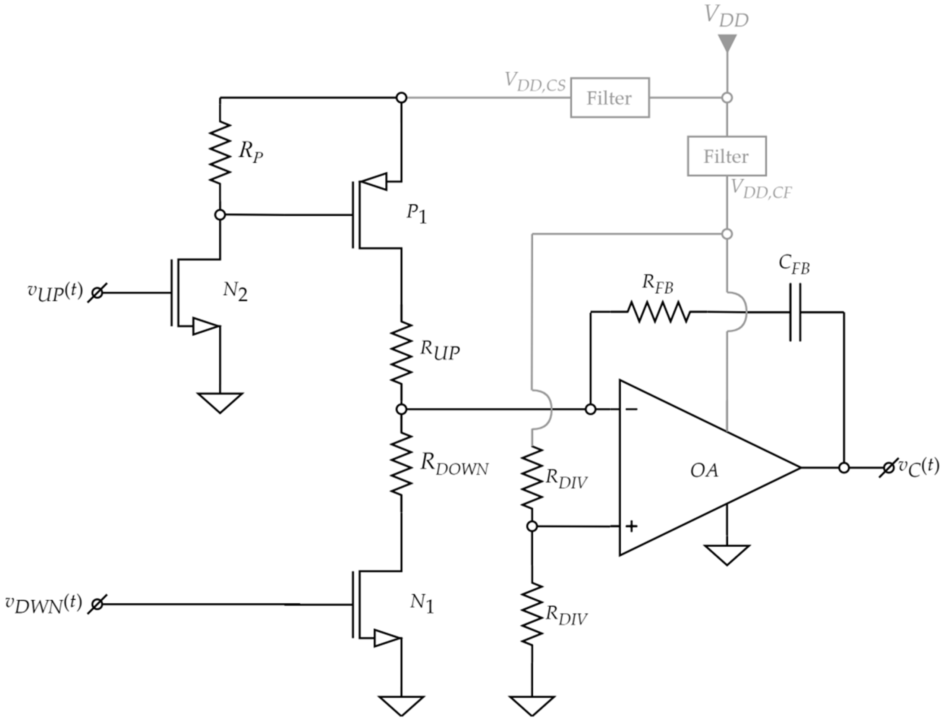
2.3.4. Charge Pump and Low-Pass Filter

The charge pump (CP) and the active low-pass Filter (LPF) are designed starting from classical topologies [45]. The proposed schematic comprising both blocks is shown in Figure 7.
The schematic in Figure 7 is powered from the high voltage supply VDD,C (as shown in Figure 3). This supply voltage must be large enough to ensure the control voltage (vC(t)) range necessary for the MOS hydrogen sensor bias.
The operational amplifier (OA) from Figure 7 needs to have a large bandwidth to operate correctly at the targeted PLL frequency of 1 MHz. OA is connected in a low-pass configuration [33] with CFB, RFB in its negative feedback loop and resistors RUP and RDWN at its input. The two identical RDIV resistors set the input common mode of the amplifier at:
v ( t ) v + ( t ) = v D D , C F 2 v D D , C 2
The role of this LPF is to ensure PLL stability at the imposed operating frequency [31,45] as well as to generate the control voltage vC(t), together with the charge pump.
The CP block requires an inverting level shifter formed with n-MOS N2 and RP, necessary for driving the gate of the pull-up p-MOS P1 within the 0–VDD,C range. An acceptable propagation delay for this simple level shifter topology can be achieved if RP is set at a low enough value. However, this leads to increased power dissipation when N2 is ON. This effect is mitigated when the PLL locks, if very short “1” pulses are generated on signals vUP(t) and vDOWN(t). Thus, in steady-state operation, the N2 ON time will be low, significantly reducing average current consumption.
The CP includes the charging stage, formed with pull-up p-MOS P1, pull-down n-MOS N1 and resistors RUP and RDWN. Using (4), constant charge (IUP) and discharge (IDWN) currents are achieved in the configuration from Figure 7 (when the respective transistors are ON):
I U P = v D D , C S v ( t ) R UP v DD , C v DD , C 2 R UP = v DD , C 2 R UP
I DWN = v ( t ) R DWN v DD , C 2 R DWN
The control voltage variation during a single oscillation cycle (ΔvC) is given by the change in the voltage across CFB (see Figure 7) as it is charged/discharged by the constant IUP or IDWN, respectively. The active times for these currents, tUP and tDWN, are given by the duty cycles of the UP and DOWN pulses (see Figure 6). Thus, ΔvC can be expressed as:
Δ v C = I DWN C FB t DWN I UP C FB t UP v DD , C 2 C FB ( t DWN R DWN t UP R UP )
With the proposed VCO, PFD, LPF and CP blocks, the negative feedback operation of the PLL described in Section 2.3.1 is validated because tUP > tDOWN, when vR(t) has a greater frequency than vO(t). Therefore, according to Relation (6), the control voltage (the sensor bias) will decrease. Consequently, the sensor capacitance will be lowered (see Figure 2), leading to an increase in the VCO frequency (per Expression (1)). The PLL thus ensures that the VCO frequency follows the reference signal frequency. When the PLL locks onto the reference frequency, the control voltage no longer changes (ΔvC = 0). Therefore:
Δ v C = 0 t DWN R DWN = t UP R UP t UP t DWN = R UP R DWN
Relation (8) shows that when the proposed PLL is locked, the ratio between the duration of the UP and DOWN pulses is constant. If RUP is chosen equal to RDWN, the duration of the two pulses will also have to be equal. The PFD structure from Figure 5 cannot generate UP and DOWN pulses of equal duration unless both are very short. This is because as soon as both signals go to logic “1”, the flip-flops are reset to “0” (see also Figure 6). Therefore, to ensure power efficiency, RDOWN = RUP is a necessary condition. In this case, the PLL will drive the VCO to generate a signal vO(t) that is in phase with the reference signal vR(t).
Regarding component choice, the transistor switches from Figure 7 must have low input capacitance/gate charge as well as low turn-on and turn-off times. These requirements are similar to those imposed in the PFD design to have a very low PLL loop delay. Furthermore, the n-MOS transistors must have a threshold voltage significantly below the chosen VDD value of 2.7 V, so that vUP(t) and vDOWN(t) signals can drive them into the ON-state. At the same time, they must be able to withstand drain-source voltages equal to VDD,C.
Considering the previous considerations regarding PLL stability and CP operation, the components from Table 3 are chosen.

3. Results

This section presents the measured results for the MOS hydrogen sensors, as well as readout circuit simulations and experimental results for the entire proposed system. Initially, the measurement setup is described.

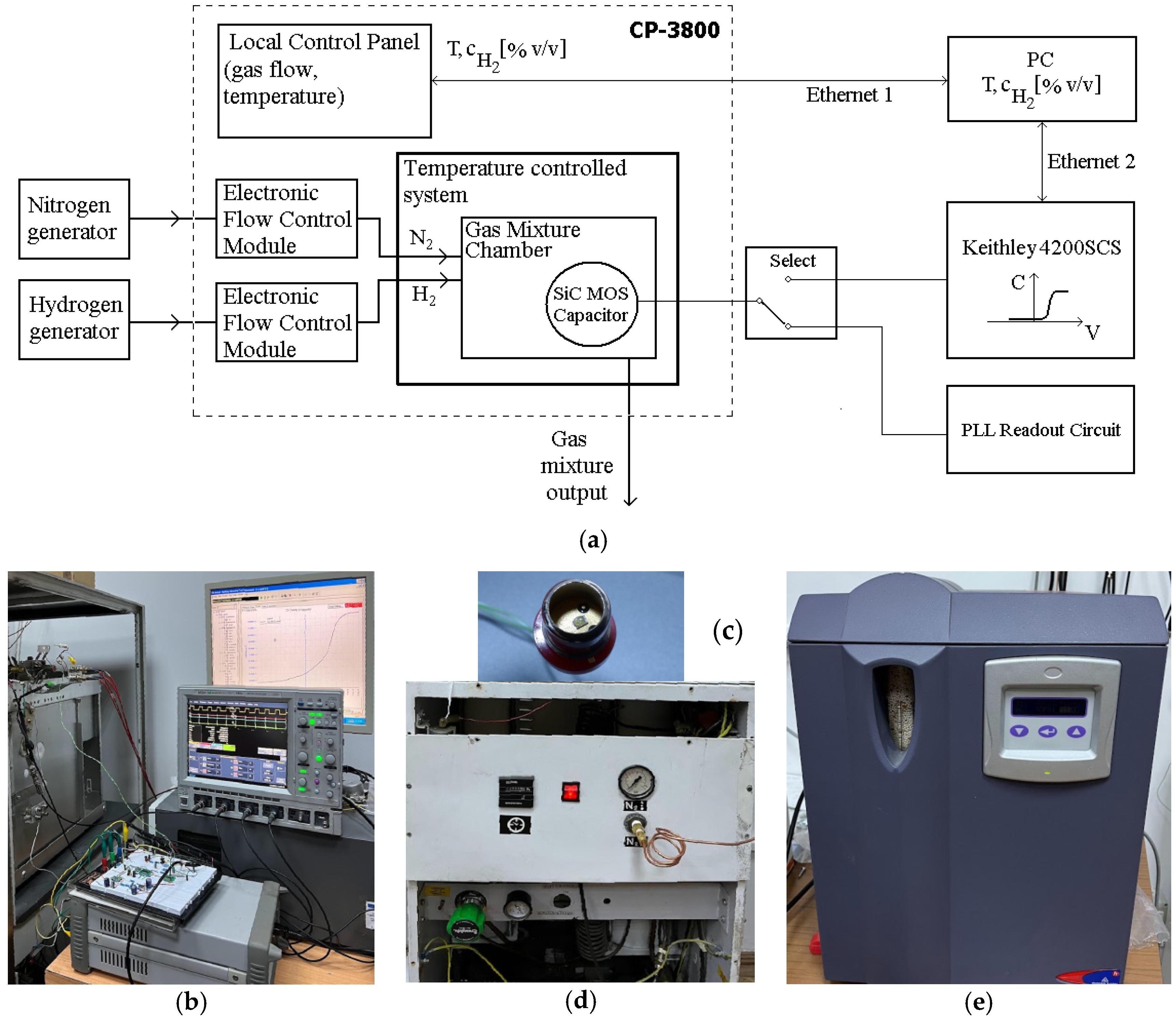
3.1. Measurement Setup

The measurement setup for the hydrogen detection system (block schematic and actual implementation) is depicted in Figure 8. It comprises a Varian CP-3800 chromatograph gas oven (for gas and temperature control) and a Keithley 4200 Semiconductor Characterization System (SCS) for MOS structure bias and C-V measurements (Figure 8b), as well as nitrogen (Figure 8d) and hydrogen (Figure 8e) generators. PLL signals are acquired using a digital oscilloscope (Figure 8b). When the PLL Readout Circuit is connected to the MOS capacitor (Figure 8c), the SCS is decoupled (Figure 8a).
The gases are controlled by mass flow controllers with integrated flow meters. The gas control unit is an adapted version of those used in gas chromatography analytical detectors and can set hydrogen concentrations between 0 and 1600 ppm with steps of 400 ppm.

3.2. Experimental Sensor Characteristics

MOS sensor C-V characteristics were extracted using a Keithley 4200-SCS Parameter Analyzer. The measurements were taken at 1 MHz and 100 °C (higher sensor temperature increases sensitivity [16]). Curves were acquired first in an inert N2 atmosphere, then with a 1600 ppm H2 concentration. Characteristics for a sample (S1) are shown in Figure 9.
The curves from Figure 9 demonstrate a sensor behavior similar to the one predicted by the theoretical characteristics from Figure 2: as the hydrogen concentration is increased, the C-V plot is variably shifted to the left. Thus, vC(t) = VG ≅ 5.3 V in inert gas is moved towards approx. 4.55 V at 1600 ppm H2 (for Cg = 96.8 pF = const).
Sensor sensitivity (S) is defined as this VG dependence on hydrogen concentration (cH2):
S = Δ v G Δ C H 2 | C g = const
Figure 9 shows that good structure sensitivity can be achieved if the PLL biases the sensor with an initial control voltage vC(t) = VG between 3 and 6 V.
Sensor response and, especially, its specificity can be affected by a number of environmental interferences, among which air humidity is the most prominent [20]. To evince this effect for our structures, the S1 sample was characterized in three consecutive days at H2 concentrations up to 1600 ppm. Figure 10 presents the SiC MOS capacitor’s voltage shift for each session. The first and third measurement (S1-M1, S1-M3) sets were acquired with the sensor introduced into the test chamber directly from ambient air, while for the second set (S1-M2), the sensor was first kept in the N2 atmosphere for 8 h at 100 °C. The baseline sensor bias was tuned for each measurement set to ensure optimal sensitivity (e.g., VG ≅ 5.3 V for S1-M1, with C-V characteristics depicted in Figure 9).
Figure 10 suggests that exposure to humid environmental air leads the MOS structure to adsorb water vapor, reducing the number of states available for hydrogen detection (S1-M1, S1-M3). Prior treatment of the sensor in a heated atmosphere releases those states and increases H2 sensitivity (S1-M2).

3.3. PLL Readout Circuit Simulation Results

The proposed VCO structure (the core of the PLL) was previously validated by simulations and experimentally [33]. It was shown to be able to generate a small-signal AC voltage across the sensor (−70 mV peak-to-peak), achieving the design target specified in Section 2.3.1. The focus in this section is on the operation of the PLL system as a whole (Figure 3).
First, the time-domain behavior of the PLL-based circuit was investigated, via transient simulations. Hence, a nonlinear capacitor model was created for the MOS sensor [45] based on the characteristic in inert gas from Figure 9.
Figure 11 presents simulated PLL waveforms. The frequency of the reference signal vR(t) (Figure 3) is set to 965 kHz. The control voltage vC(t) (panel 3, in red) is constant, which indicates that the PLL is locked. Another indication of the PLL lock is the fact that the DOWN (panel 4, in blue) and UP (panel 5, in green) signals are nearly identical periodic short “1” pulses, as anticipated in Section 2.3.4. This behavior suggests that the VCO digital output signal OSC (panel 1, in yellow, also, see vOSC(t) in Figure 5) is in phase with the digital reference input signal REF (vREF(t), panel 2, in magenta).
It is important to note that simulations in Figure 11 were carried out with separation resistor RS set to 4 kΩ. This was required because if a lower value is used, the switching noise seen on the vC(t) signal propagates to vG(t) and also affects the VCO output signal vO(t). Consequently, in simulations the PLL does not lock when RS is set to 2 kΩ (Table 1).
The simulations from Figure 11 were repeated, varying the input reference signal frequency. The control voltage was evaluated for multiple frequencies when the PLL locks resulting in the constant output voltage vC(t) vs. frequency characteristic from Figure 12.
The shape of the vC-f characteristic from Figure 12 is determined by the nonlinear sensor characteristic from Figure 9 (through the VCO). The possible control voltage range given by the PLL is between 1 and 7 V (limited by the active filter OA output range). However, above 6 V, the MOS sensor capacitance variation with bias voltage is greatly reduced (see Figure 8), so the PLL requires long simulation times to lock. For this reason, no data points with vC(t) > 6 V were included. Note that a reference frequency of 965 kHz is associated with a control voltage around 4 V.
The characteristic in Figure 12 illustrates the capability of the proposed circuit to vary the control voltage to match the internal VCO frequency to the reference frequency. This demonstrates its correct operation as a phase locked loop.

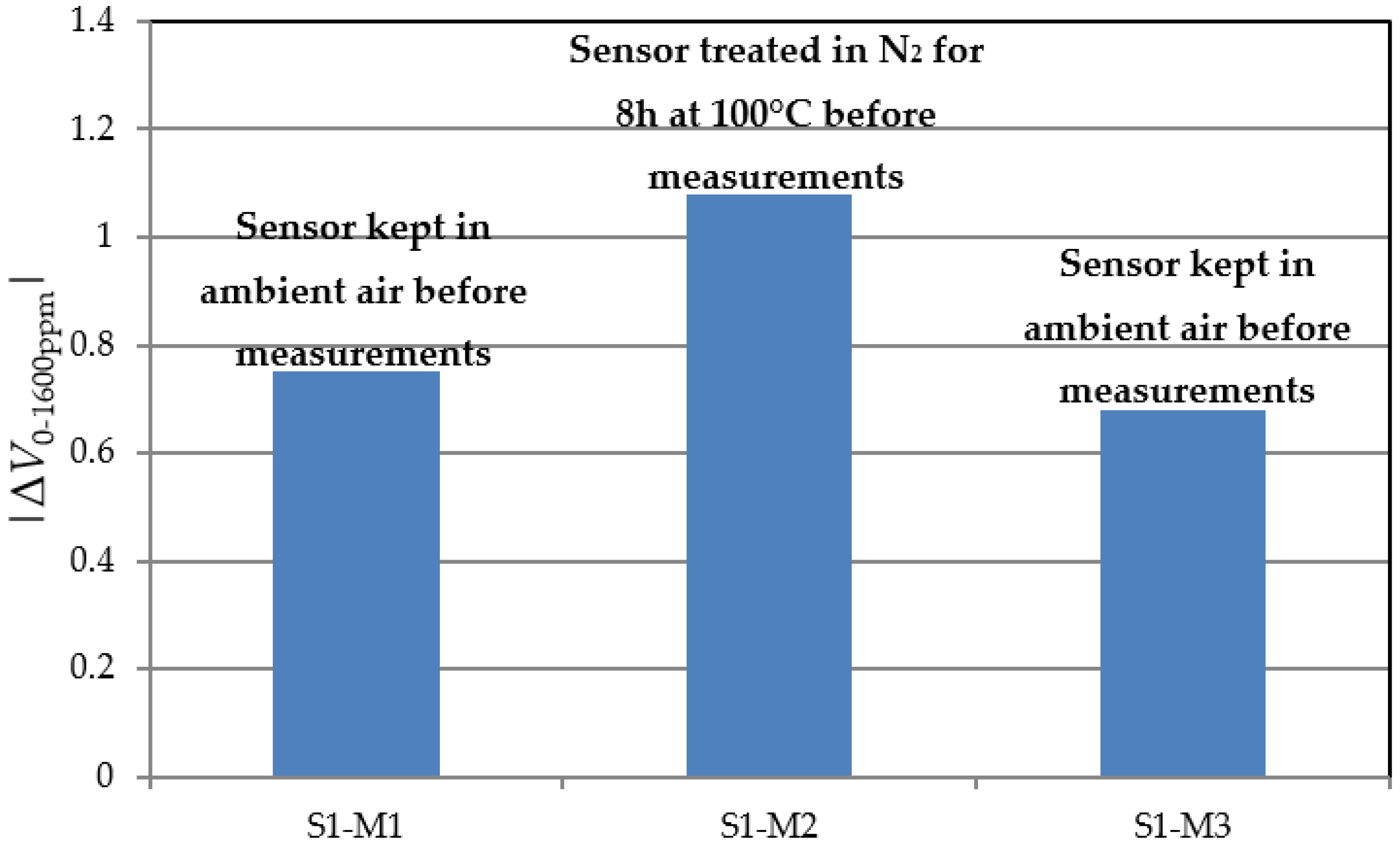
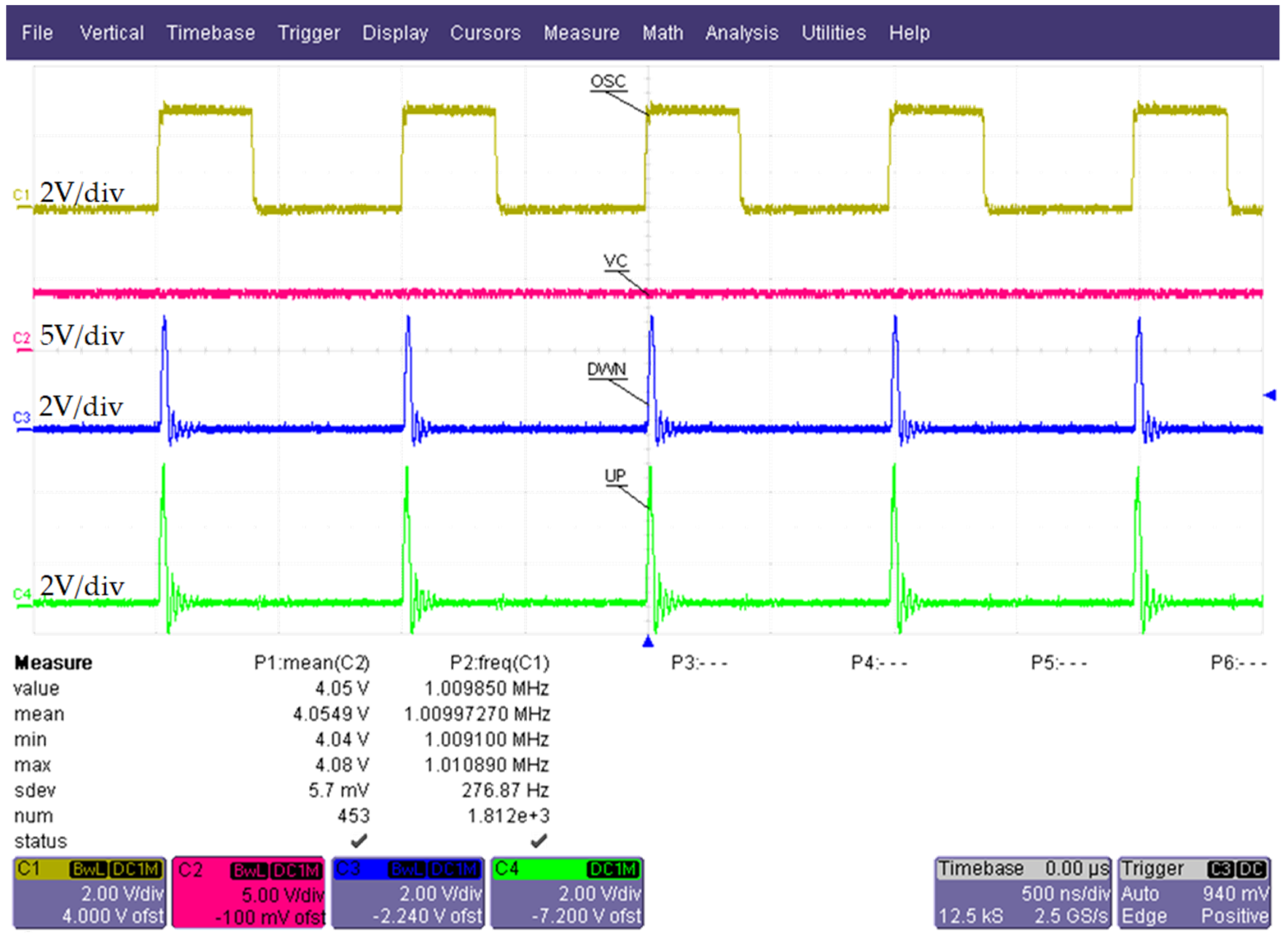
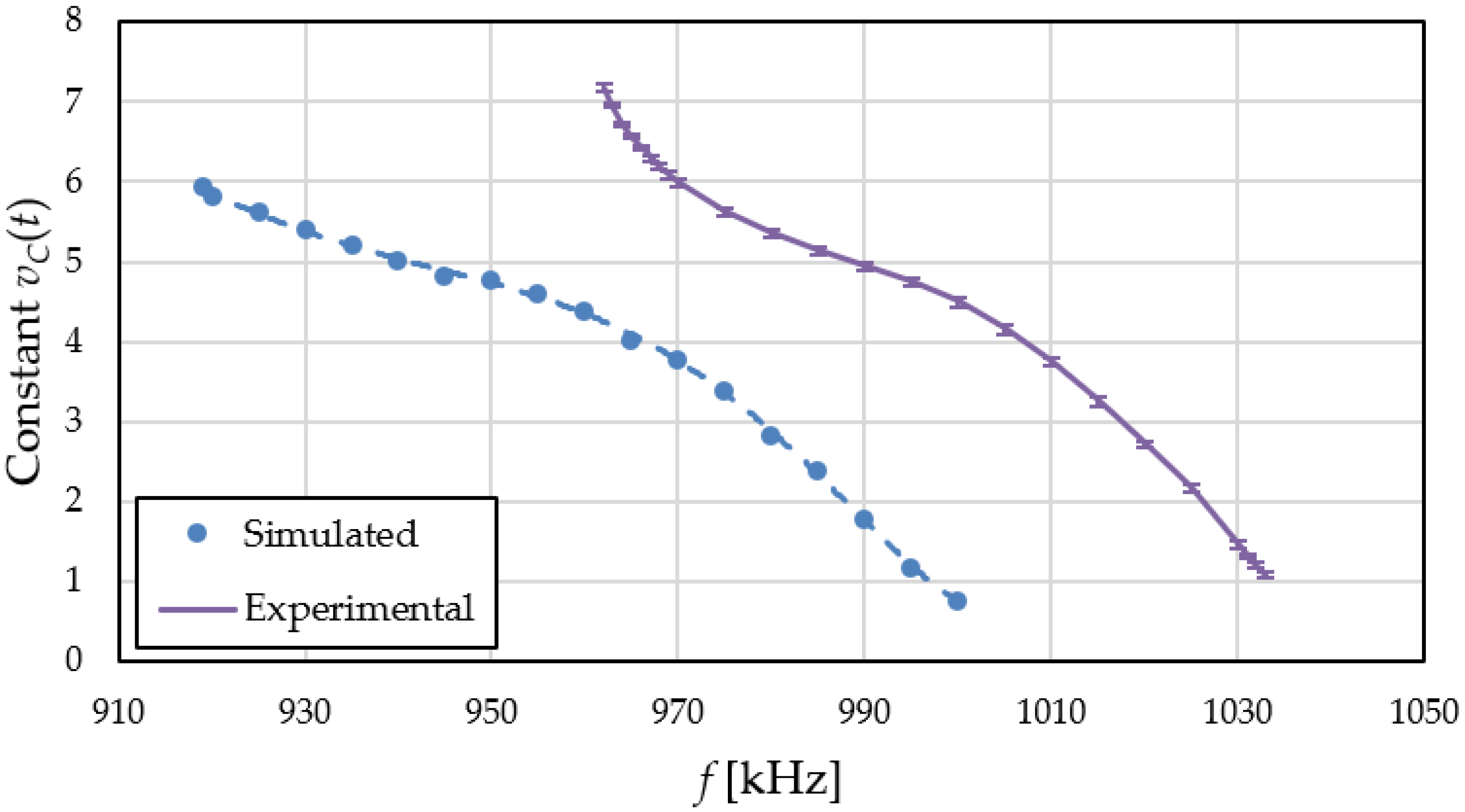
3.4. Hydrogen Detection System Measurement Results

As with simulations (Figure 11), the time-domain behavior of the proposed system was confirmed, under lock conditions. Its correct operation is demonstrated by the oscilloscope waveforms represented in Figure 13. The measurement was carried out with no H2 stimulus on the MOS sensor and with a vR frequency f 1.01 MHz.
In Figure 13 the constant control voltage vC(t) (channel 2, in pink) and the short DOWN (channel 3, in blue) and UP (channel 4, in green) pulses indicate that the PLL is locking correctly. Moreover, oscilloscope measurements P1 (vC(t) mean value) and P2 (OSC signal frequency) show that for a control voltage of approximately 4 V, the VCO outputs a center frequency of around 1 MHz, close to simulated results (Figure 11). Thus, the design target described in Section 2.3.2 was achieved experimentally (with the components from Table 1).
Furthermore, the measured average current consumption from the VDD,C supply (see Figure 3) with locked PLL is roughly 7 mA. This validates the hypothesis that the simple N2, RP level shifter from the charge pump (Figure 7) does not lead to increased steady-state power consumption.
It should be noted that the waveforms from Figure 13 were obtained with separation resistor RS (Figure 4) set to 2 kΩ (as seen in Table 1). When RS is set to 4 kΩ (shown to work in the simulation), the PLL locks very slowly or not at all. In this scenario, oscilloscope measurements show that vC(t) became less stable (oscillating within −1–2 V of its expected constant value). Thus, the PLL bandwidth decrease due to increasing RS from 2 kΩ to 4 kΩ is not acceptable experimentally (RS is part of an RC filter at the VCO input). This suggests that the cutoff frequency of the RC filter is already lower than in the simulation as a result of the equivalent VCO capacitance being larger (due to board parasitics, component tolerances and a higher input capacitance of transistor Q, Figure 4).
The measurements from Figure 13 were repeated, just as with simulations, while varying the input reference signal frequency, with no H2 stimulus. The control voltage was measured for multiple frequencies, resulting in the experimental vC-f characteristic from Figure 14. The error bars were obtained by extracting the characteristic 6 times, with the circuit being powered off between measurements.
The experimental vC-f characteristic shows a similar behavior with the simulated one. However, in Figure 14 the entire possible vC(t) range is covered by varying the frequency in a band of −70 kHz (the VCO bandwidth). Looking at Figure 12, the same band is over 80 kHz. Since the MOS sensor capacitance Cg(VG) is identical in simulations and measurements, the lower experimental bandwidth means that the VCO is less sensitive to its variation. Based on expression (2), this can be attributed to an actual C3 + CIN capacitance larger than predicted. This further validates the increased VCO capacitance as the reason for RS having to be lower in implementation.
The low voltage errors (<100 mV) observed over the entire frequency range (Figure 14) demonstrate the stability and accuracy of the proposed PLL-based readout circuit.
Figure 15 shows detection system experiments. The MOS sensors’ voltage variation at Cg = const was assessed by both the PLL readout circuit and Keithley 4200 for hydrogen concentrations between 0 and 1600 ppm, increasing every 6 min with a step of 400 ppm. The control voltage was acquired 5 min after setting the concentration to a certain step to allow the generation system to settle. Extending the exposure time past 6 min for a certain concentration would lead to sensor saturation and insensitivity past that point.
Figure 15a illustrates results for three analyzed MOS capacitor structures. For sample S1, the PLL output voltage falls by roughly 0.77 V over the entire H2 concentration range. Note that this variation in control voltage is nearly identical to Keithley 4200 measured C-V characteristics corresponding to Cg = 96.8, pF = const. (0.75 V, see Figure 8). Similar agreement was obtained for S2 and S3. Figure 15b details vC dependence on H2 concentration for sample S1 across multiple sets of measurements. The system is sensitive up to 800 ppm H2 concentration, only. Past this threshold, the states of the MOS structure become heavily occupied by hydrogen atoms, and sensitivity decreases dramatically.
Thus, the response of the proposed PLL is comparable to the one predicted by the Keithley 4200 MOS sensor measurements, and its correct operation as a readout circuit is validated.

4. Conclusions

A hydrogen detection system with a dedicated readout circuit based on a digital phase locked loop topology for SiC-MOS capacitor sensors was designed, simulated, implemented and tested. Readout blocks are essential for industrial applications, ensuring high accuracy, proper signal to noise ratio and portability. The proposed PLL schematic comprises a phase frequency detector, a voltage controlled oscillator and an active low-pass filter with charge pump. The MOS sensor is included within the VCO, and, in the presence of hydrogen, its small-signal capacitance will vary, thus leading to an oscillation frequency shift. This change is detected by the PFD, which through the LPF with CP adjusts the control voltage of the VCO (within the 1–7 V range) to maintain a frequency equal to that of the reference signal. In this manner, the readout circuit generates an output voltage proportional to the H2 concentration detected by the sensor. It applies a small AC voltage (−70 mV peak-to-peak) across the MOS sensor, a critical requirement for accurate detection. Moreover, the circuit was shown to reach a VCO frequency equal to the standard C-V characterization frequency of roughly 1 MHz at a control voltage of 4 V, evincing a good agreement between simulations and measurements.
Hydrogen measurements showed PLL control voltage shifts comparable to the variations predicted by the C-V characteristics of all investigated MOS sensor samples. Thus, the correct operation of the proposed PLL-based readout circuit was validated.
The hydrogen detection system’s obtained response variance is attributed mainly to the behavior of the SiC MOS capacitor. Structural optimizations will have to be carried out to improve its resilience to environmental conditions, such as ambient humidity.

Author Contributions

Conceptualization, F.D., F.M. and A.E.; methodology, A.E., F.M. and F.D.; software, A.E.; validation, F.D., G.B. and G.P.; formal analysis, A.E.; investigation, F.D. and A.E.; resources, G.B., F.D., F.M. and M.P.; data curation, A.E.; writing—original draft preparation, A.E. and R.P.; writing—review and editing, G.B., G.P. and A.E.; visualization, G.B., G.P. and A.E.; supervision, G.B.; project administration, G.B. and F.D.; funding acquisition, G.B. and F.D. All authors have read and agreed to the published version of the manuscript.

Funding

This research was supported in part by the PN-III-P1-1.2-PCCDI Romanian project under the contract SENSIS no. 71PCCDI ⁄ 2018 and in part by the PN-III-P2-2.1-PED-2019 Romanian Project under contract SiC-HITs 275PED/2020. Additionally, this work was supported by a grant of the Romanian Ministry of Education and Research, CNCS–UEFISCDI, project number PN-III-P1-1.1-PD-2019-0924, within PNCDI III.

Institutional Review Board Statement

Not applicable.

Informed Consent Statement

Not applicable.

Data Availability Statement

Not applicable.

Acknowledgments

The authors thank P. Varasteanu for schematic view of the test structures (Figure 1).

Conflicts of Interest

The authors declare no conflict of interest.

References

  1. Ji, H.; Zeng, W.; Li, Y. Gas sensing mechanisms of metal oxide semiconductors: A focus review. Nanoscale 2019, 11, 22664–22684. [Google Scholar] [CrossRef] [PubMed]
  2. Okolie, J.A.; Patra, B.R.; Mukherjee, A.; Nanda, S.; Dalai, A.K.; Kozinski, J.A. Futuristic applications of hydrogen in energy, biorefining, aerospace, pharmaceuticals and metallurgy. Int. J. Hydrogen Energy 2021, 46, 8885–8905. [Google Scholar] [CrossRef]
  3. Fan, L.; Tu, Z.; Chan, S.H. Recent development of hydrogen and fuel cell technologies: A review. Energy Rep. 2021, 7, 8421–8446. [Google Scholar] [CrossRef]
  4. Stern, A.G. A new sustainable hydrogen clean energy paradigm. Int. J. Hydrogen Energy 2018, 43, 4244–4255. [Google Scholar] [CrossRef]
  5. Brandon, N.P.; Kurban, Z. Clean energy and the hydrogen economy. Philos. Trans. R. Soc. A Math. Phys. Eng. Sci. 2017, 375, 20160400. [Google Scholar] [CrossRef]
  6. Hijikata, T. Research and development of international clean energy network using hydrogen energy (WE-NET). Int. J. Hydrogen Energy 2002, 27, 115–129. [Google Scholar] [CrossRef]
  7. Lee, D.-H.; Hung, C.-P. Toward a clean energy economy: With discussion on role of hydrogen sectors. Int. J. Hydrogen Energy 2012, 37, 15753–15765. [Google Scholar] [CrossRef]
  8. Chalk, S.G.; Miller, J.F. Key challenges and recent progress in batteries, fuel cells, and hydrogen storage for clean energy systems. J. Power Sources 2006, 159, 73–80. [Google Scholar] [CrossRef]
  9. Rohland, B.; Nitsch, J.; Wendt, H. Hydrogen and fuel cells—The clean energy system. J. Power Sources 1992, 37, 271–277. [Google Scholar] [CrossRef]
  10. Peraldo Bicelli, L. Hydrogen: A clean energy source. Int. J. Hydrogen Energy 1986, 11, 555–562. [Google Scholar] [CrossRef]
  11. Ajayan, J.; Nirmal, D.; Ramesh, R.; Bhattacharya, S.; Tayal, S.; Joseph, L.L.; Thoutam, L.R.; Ajitha, D. A critical review of AlGaN/GaN-heterostructure based Schottky diode/HEMT hydrogen (H2) sensors for aerospace and industrial applications. Measurement 2021, 186, 110100. [Google Scholar] [CrossRef]
  12. Kashif, M.; Ali, M.E.; Ali, S.M.U.; Hashim, U.; Hamid, S.B.A. Impact of hydrogen concentrations on the impedance spectroscopic behavior of Pd-sensitized ZnO nanorods. Nanoscale Res. Lett. 2013, 8, 68. [Google Scholar] [CrossRef] [PubMed] [Green Version]
  13. Wadell, C.; Nugroho, F.A.A.; Lidström, E.; Iandolo, B.; Wagner, J.B.; Langhammer, C. Hysteresis-Free Nanoplasmonic Pd–Au Alloy Hydrogen Sensors. Nano Lett. 2015, 15, 3563–3570. [Google Scholar] [CrossRef] [PubMed]
  14. Yew, C.K. Silicon carbide (SiC)-based sensors for harsh environment applications. Jurutera Inst. Eng. Malays. 2007, 1, 22–29. [Google Scholar]
  15. Chen, L.-Y. Survey Report of Current Status of High Temperature Microdevices Packaging. 2005. Available online: https://www.semanticscholar.org/paper/Survey-Report-of-Current-Status-of-High-Temperature-Chen/d89378e50fe050ccf6dff2d6f3a3fc8bf676236a (accessed on 19 January 2022).
  16. Kim, S.; Choi, J.; Jung, M.; Joo, S.; Kim, S. Silicon Carbide-Based Hydrogen Gas Sensors for High-Temperature Applications. Sensors 2013, 13, 13575–13583. [Google Scholar] [CrossRef]
  17. Avetisov, V.; Bjoroey, O.; Wang, J.; Geiser, P.; Paulsen, K.G. Hydrogen Sensor Based on Tunable Diode Laser Absorption Spectroscopy. Sensors 2019, 19, 5313. [Google Scholar] [CrossRef] [Green Version]
  18. Jung, S.-W.; Lee, E.K.; Kim, J.H.; Seung-Yun Lee, S.-Y. High-concentration Nafion-based hydrogen sensor for fuel-cell electric vehicles. Solid State Ion. 2020, 344, 115–134. [Google Scholar] [CrossRef]
  19. Buttner, W.; Rivkin, C.; Burgess, R.; Hartmann, K.; Bloomfield, I.; Bubar, M.; Post, M.; Boon-Brett, L.; Weidner, E.; Moretto, P. Hydrogen monitoring requirements in the global technical regulation on hydrogen and fuel cell vehicles. Int. J. Hydrogen Energy 2017, 42, 7664–7671. [Google Scholar] [CrossRef] [Green Version]
  20. Chappanda, K.N.; Tchalala, M.R.; Shekhah, O.; Surya, S.G.; Eddaoudi, M.; Salama, K.N. A Comparative Study of Interdigitated Electrode and Quartz Crystal Microbalance Transduction Techniques for Metal–Organic Framework-Based Acetone Sensors. Sensors 2018, 18, 3898. [Google Scholar] [CrossRef] [Green Version]
  21. Pascu, R.; Kusko, M.; Craciunoiu, F.; Pristavu, G.; Brezeanu, G.; Badila, M.; Avramescu, V. A new 4H-SiC hydrogen sensor with oxide ramp termination. Mater. Sci. Semicond. Process. 2016, 42, 268–272. [Google Scholar] [CrossRef]
  22. Pascu, R.; Craciunoiu, F.; Pristavu, G.; Brezeanu, G.; Kusko, M. Oxide trap states versus gas sensing in SiC-MOS capacitors—The effect of N- and P- based post oxidation processes. Sens. Actuators B Chem. 2017, 245, 911–922. [Google Scholar] [CrossRef]
  23. Andersson, M.; Lloyd Spetz, A.; Puglisi, D. Chapter Ten—Recent progress in silicon carbide field effect gas sensors. In Semiconductor Gas Sensors, 2nd ed.; Woodhead Publishing Series in Electronic and Optical Materials; Woodhead Publishing: Sawston, UK, 2020; pp. 309–346. ISBN 9780081025598. [Google Scholar] [CrossRef]
  24. Soo, M.T.; Cheong, K.Y.; Ahmad Fauzi Mohd Noor, A.F.M. Advances of SiC-based MOS capacitor hydrogen sensors for harsh environment applications. Sens. Actuators B Chem. 2010, 151, 39–55. [Google Scholar] [CrossRef]
  25. Aval, L.F.; Elahi, S.M. Hydrogen gas detection using MOS capacitor sensor based on palladium nanoparticles-gate. Electron. Mater. Lett. 2017, 13, 77–85. [Google Scholar] [CrossRef]
  26. Draghici, F.; Brezeanu, G.; Pristavu, G.; Pascu, R.; Badila, M.; Pribeanu, A.; Ceuca, E. 400 °C Sensor Based on Ni/4H-SiC Schottky Diode for Reliable Temperature Monitoring in Industrial Environments. Sensors 2019, 19, 2384. [Google Scholar] [CrossRef] [PubMed] [Green Version]
  27. Enache, A.; Rusu, I.; Draghici, F.; Pristavu, G.; Brezeanu, G.; Enache, F. High Accuracy Amperometric Sense and Control Circuit for Three-electrode Biosensors. Rom. J. Inf. Sci. Technol. 2016, 19, 295–308. [Google Scholar]
  28. Zhao, W.; Li, S.; Xu, B.; Yang, X.; Tang, X.; Shen, L.; Lu, N.; Pan, D.Z.; Sun, N. A 0.025-mm2 0.8-V 78.5-dB SNDR VCO-Based Sensor Readout Circuit in a Hybrid PLL- ΔΣ M Structure. IEEE J. Solid-State Circuits 2019, 55, 666–679. [Google Scholar] [CrossRef]
  29. Quintero, A.; Cardes, F.; Perez, C.; Buffa, C.; Wiesbauer, A.; Hernandez, L. A VCO-Based CMOS Readout Circuit for Capacitive MEMS Microphones. Sensors 2019, 19, 4126. [Google Scholar] [CrossRef] [Green Version]
  30. Chand, R.; Tanaka, S.; Esashi, M. Silicon carbide diode bridge circuit for capacitive sensor readout in high temperature (673K) environment. In Proceedings of the Transducers & Eurosensors XXVII—The 17th International Conference on Solid-State Sensors, Actuators and Microsystems, Barcelona, Spain, 16–20 June 2013; pp. 1020–1023. [Google Scholar] [CrossRef]
  31. Best, R.E. Phase-Locked Loops: Design, Simulation, and Application; McGraw-Hill Education: New York, NY, USA, 2007. [Google Scholar]
  32. Gray, P.; Hurst, P.; Lewis, S.; Meyer, R. Analysis and Design of Analog Integrated Circuits, 4th ed.; John Wiley & Sons: New York, NY, USA, 2001. [Google Scholar]
  33. Enache, A.; Drăghici, F.; Pristavu, G.; Brezeanu, G. Voltage Controlled Oscillator for Small-Signal Capacitance Sensing. In Proceedings of the 2019 International Semiconductor Conference (CAS), Sinaia, Romania, 9–11 October 2019; pp. 323–326. [Google Scholar] [CrossRef]
  34. Kang, C.-W.; Moon, H.; Yang, J.-R. Switched-Biasing Techniques for CMOS Voltage-Controlled Oscillator. Sensors 2021, 21, 316. [Google Scholar] [CrossRef]
  35. Rothbart, N.; Hübers, H.-W.; Schmalz, K.; Borngräber, J.; Kissinger, D. Towards Breath Gas Analysis Based on Millimeter-Wave Molecular Spectroscopy. Frequenz 2018, 72, 87–92. [Google Scholar] [CrossRef]
  36. Schmalz, K.; Rothbart, N.; Eissa, M.H.; Borngräber, J.; Kissinger, D.; Hübers, H.-W. Transmitters and receivers in SiGe BiCMOS technology for sensitive gas spectroscopy at 222–270 GHz. AIP Adv. 2019, 9, 015213. [Google Scholar] [CrossRef] [Green Version]
  37. Kissinger, D.; Rothbart, N.; Schmalz, K.; Borngräber, J.; Hübers, H.-W. Sensitive Millimeter-Wave/Terahertz Gas Spectroscopy Based on SiGe BiCMOS Technology. In Proceedings of the 43rd International Conference on Infrared, Millimeter, and Terahertz Waves (IRMMW-THz), Nagoya, Japan, 9–14 September 2018. [Google Scholar] [CrossRef]
  38. Kumar, V.; Mishra, S.V.N.; Dwivedi, R.; Das, R.R. Influence of gridded gate structure on gas sensing behavior of hydrogen. J. Appl. Phys. 2014, 115, 204514. [Google Scholar] [CrossRef]
  39. Lua, C.; Chen, Z. MOS hydrogen sensor with very fast response based on ultra-thin thermal SiO2 film. Int. J. Hydrogen Energy 2010, 35, 12561–12567. [Google Scholar] [CrossRef]
  40. Irokawa, Y.; Usami, M. First-principles studies of hydrogen adsorption at Pd-SiO2 interfaces. Sensors 2015, 15, 14757–14765. [Google Scholar] [CrossRef] [PubMed] [Green Version]
  41. Grebennikov, A. RF and Microwave Transistor Oscillator Design; John Wiley & Sons: New York, NY, USA, 2007. [Google Scholar]
  42. Datasheet SS9018 NPN Epitaxial Silicon Transistor. Available online: https://www.onsemi.com/pdf/datasheet/ss9018-d.pdf (accessed on 19 January 2022).
  43. Datasheet PWB-2-CL Surface Mount Wideband RF Transformers. Available online: https://www.coilcraft.com/getmedia/2623c26b-542e-49f8-90ee-c7b1fe27d34b/pwb.pdf (accessed on 19 January 2022).
  44. Razavi, B. Design of Analog CMOS Integrated Circuits; McGraw-Hill Education: New York, NY, USA, 2002. [Google Scholar]
  45. Enache, A. Prelucrarea Semnalelor de la Ieșirea Senzorilor de Gaz Cu Circuite PLL. Ph.D. Thesis, University Politehnica of Bucharest, Bucharest, Romania, 2018. [Google Scholar]
  46. Datasheet SN74LVC125A Quadruple Bus Buffer Gate With 3-State Outputs. Available online: https://www.ti.com/lit/ds/symlink/sn74lvc125a.pdf (accessed on 19 January 2022).
  47. Datasheet SN74LVC74A Dual Positive-Edge-Triggered D-Type Flip-Flops with Clear and Preset. Available online: https://www.ti.com/lit/ds/symlink/sn74lvc74a.pdf (accessed on 19 January 2022).
  48. Datasheet SN74LVC1G00 Single 2-Input Positive-NAND Gate. Available online: https://www.ti.com/lit/ds/symlink/sn74lvc1g00.pdf (accessed on 19 January 2022).
  49. Datasheet FDC6301N N-Channel Digital FET. Available online: https://www.onsemi.com/pdf/datasheet/fdc6301n-d.pdf (accessed on 19 January 2022).
  50. Datasheet FDC6302P P-Channel Digital FET. Available online: https://www.onsemi.com/pdf/datasheet/fdc6302p-d.pdf (accessed on 19 January 2022).
  51. Datasheet LT1354 12 MHz, 400 V/µs Op Amp. Available online: https://www.analog.com/media/en/technical-documentation/data-sheets/1354fa.pdf (accessed on 19 January 2022).
Figure 1. SiC MOS hydrogen sensor structure.
Sensors 22 01462 g001
Figure 2. MOS sensor C-V theoretical characteristics (in inert gas and with H2 stimulus).
Sensors 22 01462 g002
Figure 3. Proposed Digital PLL readout block schematic.
Sensors 22 01462 g003
Figure 4. Proposed Armstrong VCO schematic.
Sensors 22 01462 g004
Figure 5. Proposed digital PFD schematic.
Sensors 22 01462 g005
Figure 6. PFD waveforms: (a) REF leads OSC; (b) OSC leads REF.
Sensors 22 01462 g006
Figure 7. Proposed CP and active LPF schematic.
Sensors 22 01462 g007
Figure 8. Measurement setup for H2 detection: (a) block schematic; (b) system image; (c) SiC MOS capacitor; (d) Nitrogen generator; (e) Hydrogen generator.
Sensors 22 01462 g008
Figure 9. MOS sensor C-V experimental characteristics for sample S1: in inert gas and with 1600 ppm H2, respectively.
Sensors 22 01462 g009
Figure 10. S1 MOS sensor voltage shift after exposure to hydrogen.
Sensors 22 01462 g010
Figure 11. Simulated PLL operation: VCO digital output signal OSC (yellow); digital reference signal REF (magenta); control voltage vC(t) (red); DOWN signal vDWN(t) (blue); UP signal vUP(t) (green).
Sensors 22 01462 g011
Figure 12. Simulated PLL control voltage vs. reference frequency characteristic.
Sensors 22 01462 g012
Figure 13. Measured PLL waveforms: C1, OSC signal; C2, control voltage vC(t); C3, DOWN signal vDWN(t); C4, UP signal vUP(t).
Sensors 22 01462 g013
Figure 14. Experimental PLL control voltage vs. reference frequency characteristic alongside simulated data from Figure 10.
Sensors 22 01462 g014
Figure 15. (a) PLL output variation vs. SiC MOS capacitor voltage shift (measured with Keithley 4200); (b) experimental PLL output voltage vs. hydrogen concentration for sample S1.
Sensors 22 01462 g015
Table 1. VCO component values and types.
ComponentValue/Type
VDD2.7 V
QSS9018 (1)
R12 kΩ (2)
R26.6 kΩ
L137.5 µH (3)
L275 µH (3)
C12.2 nF
C22.2 nF
C3100 pF
RS2 kΩ
(1) High-frequency transistor, chosen for its low capacitances [42]. (2) Value used in the implemented PLL, but set to 4 kΩ in simulations (see Section 3.2 and Section 3.3). (3) Achieved using half of the windings in the transformer PWB-2-CL [43].
Table 2. PFD component values and types.
ComponentValue/Type
VDD2.7 V
Digital buffersSN74LVC125A (1)
D flip-flopsSN74LVC74A (2)
NAND gateSN74LVC1G00 (3)
RFX1 kΩ
(1) Quadruple bus buffer of which only two are used [46]. (2) Dual D flip-flops [47]. (3) Single two-input NAND gate [48].
Table 3. CP and LPF component values and types.
ComponentValue/Type
VDD,C8 V
N1FDC6301N 1
N2FDC6301N 1
P1FDC6302P 2
OALT1354 3
RP50 Ω
RUP2 kΩ
RDOWN2 kΩ
RFB250 Ω
CFB2 nF
1 n-MOS transistor with low input and output capacitances, low switching times [49]; 2 p-MOS transistor with low input and output capacitances, low switching times [50]; 3 Operational amplifier for active filters, 12 MHz gain bandwidth [51].
Publisher’s Note: MDPI stays neutral with regard to jurisdictional claims in published maps and institutional affiliations.

