
Mid-Infrared Sensor Based on Dirac Semimetal Coupling Structure

1
Institute of Semiconductors, Chinese Academy of Sciences, Beijing 100083, China
2
College of Materials Science and Opto-Electronic Technology, University of Chinese Academy of Sciences, Beijing 100049, China
3
College of Chemistry, Beijing Normal University, Beijing 100875, China
*
Author to whom correspondence should be addressed.
Sensors 2022, 22(6), 2116; https://0-doi-org.brum.beds.ac.uk/10.3390/s22062116
Submission received: 14 February 2022
/
Revised: 4 March 2022
/
Accepted: 7 March 2022
/
Published: 9 March 2022
(This article belongs to the Special Issue Nanogenerators and Self-Powered Optical Sensors)
Abstract
:A multilayer structure based on Dirac semimetals is investigated, where long-range surface plasmon resonance (LRSPR) of a dielectric layer/Dirac semimetal/dielectric layer are coupled with surface plasmon polaritons (SPPs) on graphene to substantially improve the Goos–Hänchen (GH) shift of Dirac semimetals in the mid-infrared band. This has important implications for the study of mid-infrared sensors. We studied the reflection coefficient and phase of this multilayer structure using a generalized transport matrix. We established that subtle changes in the refractive index of the sensing medium and the Fermi energy of the Dirac semimetal significantly affected the GH shift. Our numerical simulations show that the sensitivity of the coupling structure is more than , which can be used as a potential new sensor application. The novelty of this work is the design of a tunable, highly sensitive, and simple structured mid-infrared sensor that takes advantage of the excellent properties of Dirac semimetals.
1. Introduction
In condensed matter physics, topological materials have received much research interest because of their ability to contain relativistic fermions with low-energy excitations [1,2,3,4]. Dirac semimetals (DSMs) are a type of topological material, famous for their topologically protected linear dispersive energy bands. Unlike the first studied two-dimensional (2D) Dirac systems, where the graphene energy band crossings are susceptible to perturbation, the system perturbation can only slightly move the three-dimensional (3D) Dirac cone of the DSM without eliminating it, which is quite robust [5]. This unique energy band structure endows the DSM with distinctive properties that make it suitable for optoelectronic applications [6,7,8,9]. Since their theoretical prediction, numerous angle-resolved photoemission spectroscopy and scanning tunneling microscope experiments have confirmed the existence of conical features in the energy band structure [10,11,12], giving rise to a large number of subsequent theoretical and experimental follow-ups that have enriched the understanding of DSMs.
Dirac semimetals are not only scientifically attractive, but they also have many potential applications. Owing to their energy-gapless tapered energy band, they have important potential applications in high-speed, broadband optoelectronic devices owing to their ultra-high mobility and broadband optical absorption [10,13,14,15]. The mid-infrared band (2–20 ) is widely favored for scientific research due to its extremely high utility [16,17,18,19]. However, due to material limitations, it has been relatively little studied compared to the visible band. Additionally, the semi-metallic nature of DSM makes it highly promising. In the mid-infrared to terahertz band, DSM and graphene have a dielectric constant below zero, which can excite surface plasmon resonance (SPR) with less loss than conventional metals (e.g., Ag and Au) and is expected to be an excellent candidate for SPR [20,21]. Like graphene, its tunability is more prominent [22,23,24], and its thickness can be freely tailored to ensure stronger light-matter interactions.
Goos–Hänchen (GH) shifts have attracted attention for numerous studies and applications in optics, chemistry, and biomedicine [25,26,27,28,29]. However, small shifts in ordinary structures have limited their research. Currently, large GH shifts have been obtained [30,31,32] by SPR, long-range surface plasmon resonance (LRSPR), etc. In the visible band, the coupling of two electromagnetic modes can further increase the GH shift and obtain a higher sensor sensitivity [33]. Therefore, the special structure may effectively improve the GH shifts.
In this paper, we propose a Dirac semimetal-based coupling structure. The large GH shift of this coupled structure in the mid-infrared band was studied based on the generalized transfer matrix. This large GH shift can be regulated by the thickness of the coupling layer, thickness of the Dirac semimetal, and Fermi energy. We also analyzed the effect of the refractive index of the sensing medium on the GH effect, showing excellent sensing performance.
2. Theoretical Model and Method
We propose a coupling structure to improve and control GH shifts, as depicted in Figure 1. Graphene is under the prism, and the refractive index of the prism is , which is used to increase the wave vector. The second and fourth layers are the sensing medium () [34,35,36,37], and the DSM is fitted between the sensing medium. In brief, our structure can be considered as a common SPR sensor with a thin layer of Dirac semimetal immersed in the analyte solution. Graphene can be transferred to the prism with the assistance of PDMS [38].
First, we verified the SPP at the graphene/sensing medium interface. The surface conductivity of graphene can be described by the well-known Kubo formula, for [39,40,41]:
where e is elemental charge, and represent the reduced Planck constant and angular frequency of incident light, respectively; is the fermi energy, T is the temperature, and is a phenomenological scattering rate (). In the mid-infrared band, the dielectric constant of graphene is below zero, therefore it can excite SPPs instead of metals. The SPP dispersion relationship excited by the graphene/sensing medium can be expressed by the following formula [42]:
The effective dielectric constant can be defined as .
Previous studies have shown that the conductivity of the DSM can be described by the Kubo formula [21,43]. For and long-wavelength limit, the optical conductivity can be written analytically as
where g is the degeneracy factor, is the Fermi velocity, is the step function, and represents the high-energy cutoff of the linear model. Here, is the normalized frequency .
To accurately describe the dielectric function of the DSM, a two-band model considering inter-band electron transition is used instead of a simple Drude-like model [43]:
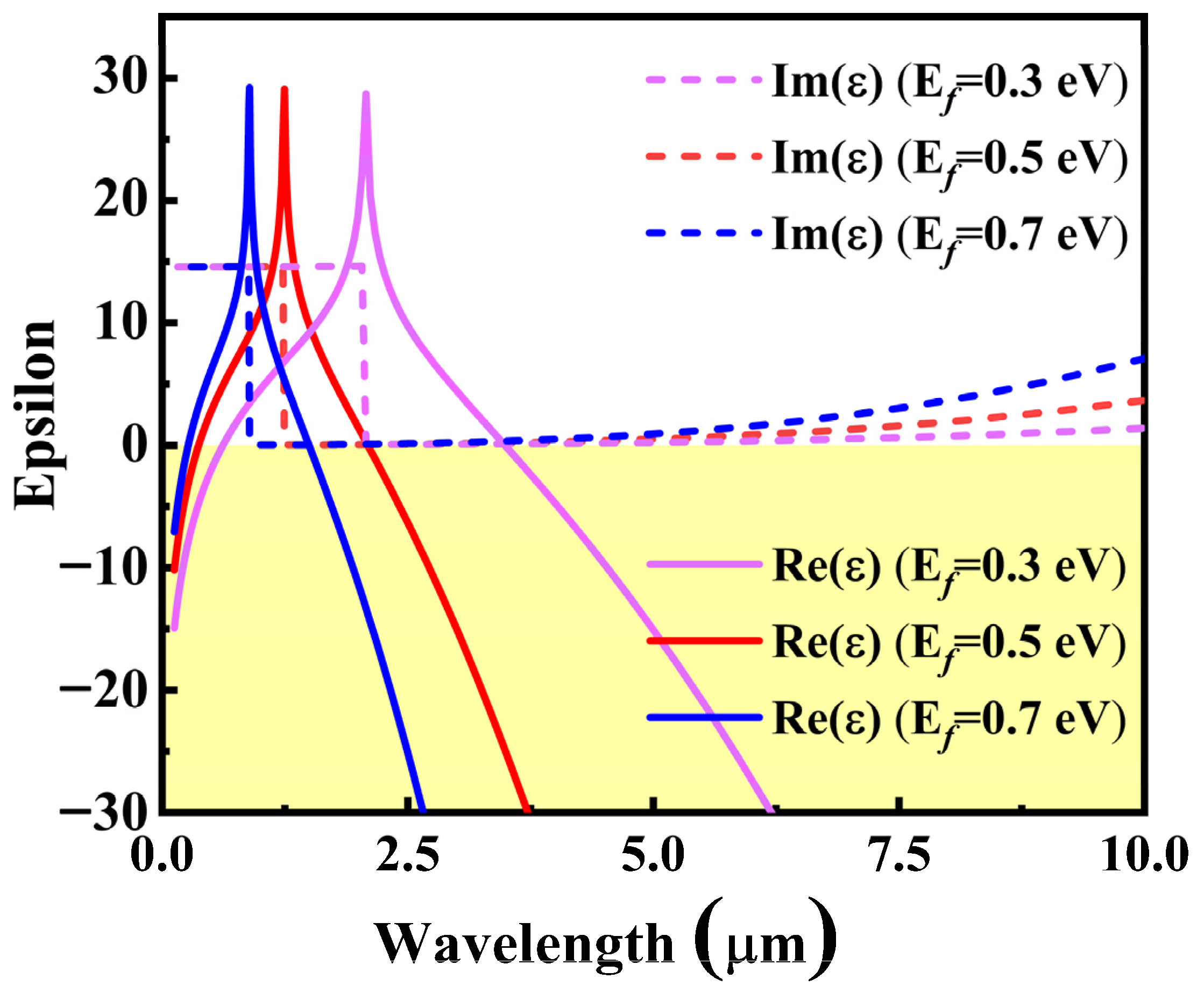
Therefore, when considering the Drude damping ( instead of ), the dielectric function of the DSM is shown in Figure 2.
In the middle infrared band, the real part of the dielectric function of the DSM is below zero and has a suitable imaginary part, which indicates a good SPP material [42]. In the case of being fitted by the sensing medium, an insulator–metal–insulator (IMI) structure can be formed to excite the LRSPR. Through the boundary conditions of the symmetrical IMI structure [42], the dispersion relationship can be derived as
where, ,.
For this coupling structure, we used a generalized transfer matrix [44] to calculate the reflectivity and phase at TM incidence. This method can deal with different types of materials arbitrarily, which does not exist in discontinuous solutions.
For multilayer systems, using the electromagnetic field boundary conditions, we can connect the electromagnetic wave amplitudes of two adjacent layers [44]:
where is the dynamic matrix with respect to the electric field vector , and is the ith layer.
To better define the transmission matrix, the propagation matrix is introduced by P [44,45]:
where is the speed of light, is the angular frequency of the incident light, and are the four eigensolutions of the z-component of the wave vector (thickness) in the layer of the material.
Thus, the transmission matrix of the whole structure can be written as
Based on the transmission matrix Q, the reflection coefficient of the TM polarization incidence can be calculated as follows [44,45]:
Here, the subscripts pp and ps represent the p and s reflections of p incidence, respectively.
After obtaining the reflection coefficient, according to the static phase method, the GH shift can be expressed as
Here, is the angle of incidence, is the wavelength, and is the reflected phase.
As is proportional to the off-diagonal components’ dielectric function, all the materials in our structure without considering the magnetic field effect. Therefore, the effect of on GH shifts could be disregarded. In the following discussion, if not otherwise specified, we set the incident light wavelength to be λ = 2.5 µm.
Sensitivity is an important parameter for precision probing, meaning the degree of change in the amount of response is due to a change in the measured quantity. As the structure is sensitive to many parameters, a variety of sensitivities can be defined. For example, the change in the angle of the GH shifts maximum with respect to the Fermi energy can be defined and used to measure the ability to detect the Fermi energy level:
Similarly, it can also be used as a refractive index sensor, and the ratio of the change in GH shifts caused by the change in refractive index of the sensing medium to the change in refractive index is used as the sensitivity:
3. Results and Discussion
Figure 3a shows the reflection coefficient and phase with the angle of incidence. When = 52.255, a narrow peak in induced by the SPR. In the region of the peak, the reflection phase changes significantly. At this wavelength, the imaginary part of the DSM dielectric constant is very small; therefore, the reflection spectrum has a small half-width (). According to Equation (10), acute phase changes within a narrow range results in large GH shifts. As shown in Figure 3b, a large GH shift of 521 λ is observed at the resonance peak.
Previous studies have reported that LRSPR can significantly reduce the half-peak width of the resonance, resulting in sharp phase changes and a significant increase in GH shifts [30]. To further increase the GH shifts, the structural coupling between graphene SPP and DSM LRSPR was used to obtain better performance. To verify that graphene SPPs can couple with LRSPR with an IMI structure, the coupling conditions were studied. When the incident light = 119 THz, the effective refractive index varies with the of the DSM, as shown in Figure 4.
Figure 4 shows that the effective refractive index of the IMI structure can be easily adjusted by of DSM, showing excellent adjustable performance. When the of the DSM is 0.5 eV, the two systems have the same effective refractive index (neff = 1.64). In this case, the two modes can be coupled, which theoretically further increases the GH shift.
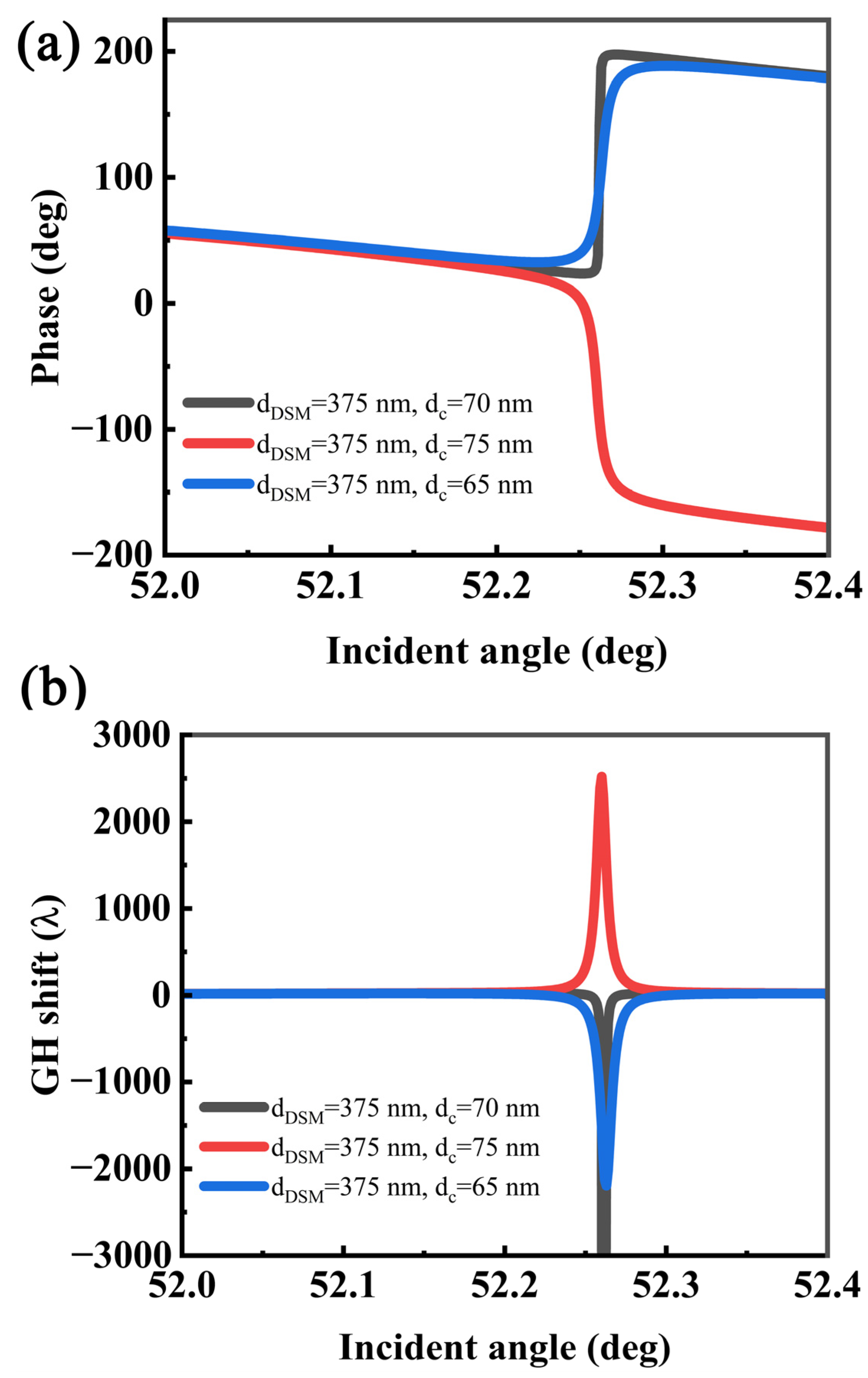
In this coupled structure, the GH shifts are affected by many factors. For example, the thickness of the metal layer in the IMI structure that excites the LRSPR, the thickness of the coupling layer, etc. As shown in Figure 5, when the coupling layer thickness and DSM thickness are selected as the optimal thickness (e.g., dDSM = 375 nm, dc = 70 nm), the phase change abruptly changes, resulting in a maximum GH shift.
In this case, however, the phase loses its physical meaning and therefore cannot accurately describe the GH shifts [46,47]. It was found that when the thickness of the coupling layer is less than the optimal thickness, the phase decreases with the increase in the angle, and when the angle of resonance increases sharply, it results in negative GH shifts. When the thickness of the coupling layer is larger than the optimal thickness, the phase increases with the increase in the incident angle, resulting in positive GH shifts. Therefore, the direction of the GH shift can be precisely controlled by adjusting the thickness of the coupling layer without significantly changing the resonance angle. We can imagine that when the coupling layer is infinite, the two modes are isolated from each other and cannot be coupled, and the GH shifts is very small. As the thickness of the coupling layer decreases, the modes start to coupling and making the GH shifts larger. As the thickness of the coupling layer continues to decrease, the optimal coupling condition is lost and the GH shift decreases again, which is consistent with previous work [33]. On the other hand, the thickness of the insulator layer of the IMI structure also affects the GH shifts [47]. Even if it deviates from the optimal thickness (dDSM = 375 nm, dc = 75 nm), the GH shift can still reach a large value of 2520 λ, which is equivalent to five times that of the ordinary DSM structure, as shown in Figure 6.
Similarly, because the thickness of the DSM affects the LRSPR, the GH shifts can also be regulated by adjusting the thickness of the DSM, as shown in Figure 7. When the thickness of the coupling layer is at a non-optimal thickness, the thickness of the DSM can also significantly change the magnitude and direction of the GH and slightly change the angle of the GH shifts to a maximum. When the thickness of the DSM is less than 375 nm, the GH shift is positive and its reflection phase decreases with the increase in angle; when the thickness of the DSM is more than 375 nm, the GH shift is negative and the phase increases with the increase in angle. As the thickness of the DSM increases, the effective permittivity of its structure also increases, which causes the maximum value of the GH to shift slightly to a high angle. When the DSM thickness is far from the optimal value, its GH peak decreases significantly, and the half-peak width increases gradually owing to the gradual loss of resonance conditions.
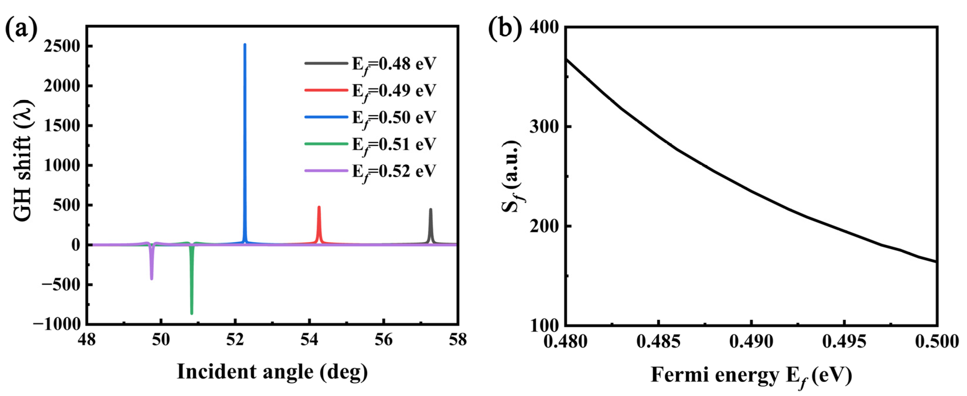
As the optical properties of Dirac semimetals are closely related to the Fermi energy, we can easily change the Fermi energy of Dirac semimetals by chemical doping, external gate electric field, etc. [48,49,50], to adjust the GH shift of the coupling structure. Similarly, this structure can not only adjust the positive and negative GH through the change in the DSM Fermi energy, but also adjust its resonance angle. This is mainly attributed to the fact that the Fermi energy significantly changes the permittivity of the DSM, which changes the effective refractive index of the structure. Additionally, the effective refractive index of the structure significantly affects the resonance angle [51]. As shown in Figure 8a, when the Fermi energy is less than 0.5 eV, the GH shift is negative, and when it is more than 0.5 eV, the GH shift is positive. We can define the Fermi energy sensitivity factor as =, and it is easy to detect subtle changes in the Fermi level, using the change in the resonance angle. When the Fermi level is changed from 0.48 eV to 0.52 eV, there is a clear change in the peak position, which has a sensitivity of more than 100 deg/eV in the range. It is easy to understand that as the Fermi level increases, the effective refractive index decreases, and its resonance angle decreases accordingly. It can be seen from Figure 4 that when the Fermi level is <0.5 eV, the effective refractive index of the IMI structure changes sharply, which can lead to a large change in the effective refractive index of the entire structure; therefore, it has a high sensitivity of more than 150°/eV in the range (in Figure 8b).
Finally, we found that a slight change in the sensing medium results in a significant change in the GH displacement; therefore, the refractive index sensor can be designed accordingly. As shown in Figure 9, we compared it with the traditional metal SPR sensor and the SPR sensor of the DSM. In the traditional Au (Ag) sensor, we used an excitation wavelength of 632.8 nm, Au (Ag) film thickness of 45 nm, and nAu = 0.7900 + 17.3109i, nAg = 0.1675 + 3.4728i. The parameters are consistent with previous studies [21,52,53]. When the refractive index of the sensing medium changes 0.002, the GH shifts changed by 51.7 .According to Equation (12), the sensitivity can be obtained as Sn . Additionally, based on the DSM structure, it has a larger while changing the smaller refractive index of the sensing medium (). Therefore, it has a higher sensitivity, Sn relative to the traditional metal sensor. The proposed coupling structure has large GH shifts compared to traditional metals. While the change in the sensing dielectric constant is very small, its GH shift changes sharply, with the purpose to obtain Sn ≈ 2.7. Compared with traditional metal sensor, it has been improved by three orders of magnitude.
Figure 10 shows the variation in sensitivity Sn with the DSM thickness and coupling layer thickness. Its GH shift is the greatest near the optimum thickness, which also results in the greatest sensitivity. As one moves away from the optimum thickness, the sensitivity decreases; however, it is still is greater than that of the conventional metallic SPR structure within a certain range, which provides a process tolerance for the actual device.
Table 1 shows the GH shifts and sensitivities of the sensors with different materials, structures, and wavelengths. Our proposed structure shows significant improvement in both GH displacement and sensitivity, providing a potential solution for mid-infrared sensors.
4. Conclusions
In this paper, we proposed a coupling structure that can greatly enhance GH displacement. In this structure, the direction of the GH displacement can be controlled independently by adjusting the thickness of the coupling layer. As the angle of GH displacement is closely related to the Fermi energy of the DSM, the change in the Fermi level can be accurately measured by the change in the GH displacement angle, and the sensitivity of the Fermi level is up to. In addition, owing to the extremely large GH displacement of the coupling structure, it can be designed as an ultra-sensitive refractive index sensor with a sensitivity up to. We believe that this sensor, based on GH shifts, has the advantages of ultra-high sensitivity and adjustability, and has potential application prospects in precision measurement, biological monitoring, etc.
Author Contributions
Conceptualization, Y.Z. and G.S.; methodology, Y.Z.; software, Y.Z.; validation, Y.Z.; formal analysis, Y.Z.; writing—review and editing, Y.Z. and Y.L.; funding acquisition, G.S. All authors have read and agreed to the published version of the manuscript.
Funding
This research was funded by the Strategic Priority Research Program of Chinese Academy of Sciences, Grant No. XDB43010000; National Natural Science Foundation of China (Grant No. 61835011); National Natural Science Foundation of China (Grant No. 12075244); Key Research Projects of the Frontier Science of the Chinese Academy of sciences (No. QYZDY-SSW-JSC004); National Science and Technology Major Project (2018ZX01005101-010); National Key Research and Development Plan (No. 2020YFB2206103).
Institutional Review Board Statement
Not applicable.
Informed Consent Statement
Not applicable.
Data Availability Statement
Not applicable.
Conflicts of Interest
The authors declare no conflict of interest.
References
- Novoselov, K.S.; Geim, A.K.; Morozov, S.V.; Jiang, D.; Katsnelson, M.I.; Grigorieva, I.V.; Dubonos, S.V.; Firsov, A.A. Two-dimensional gas of massless Dirac fermions in graphene. Nature 2005, 438, 197–200. [Google Scholar] [CrossRef] [PubMed]
- Fu, L.; Kane, C.L. Superconducting proximity effect and Majorana fermions at the surface of a topological insulator. Phys. Rev. Lett. 2008, 100, 4. [Google Scholar] [CrossRef] [PubMed] [Green Version]
- Xu, S.Y.; Belopolski, I.; Alidoust, N.; Neupane, M.; Bian, G.; Zhang, C.L.; Sankar, R.; Chang, G.Q.; Yuan, Z.J.; Lee, C.C.; et al. Discovery of a Weyl fermion semimetal and topological Fermi arcs. Science 2015, 349, 613–617. [Google Scholar] [CrossRef] [Green Version]
- Lv, B.Q.; Feng, Z.L.; Xu, Q.N.; Gao, X.; Ma, J.Z.; Kong, L.Y.; Richard, P.; Huang, Y.B.; Strocov, V.N.; Fang, C.; et al. Observation of three-component fermions in the topological semimetal molybdenum phosphide. Nature 2017, 546, 627. [Google Scholar] [CrossRef] [PubMed] [Green Version]
- Weng, H.M.; Dai, X.; Fang, Z. Topological semimetals predicted from first-principles calculations. J. Phys.-Condes. Matter 2016, 28. [Google Scholar] [CrossRef] [Green Version]
- Zhu, C.H.; Wang, F.Q.; Meng, Y.F.; Yuan, X.; Xiu, F.X.; Luo, H.Y.; Wang, Y.Z.; Li, J.F.; Lv, X.J.; He, L.; et al. A robust and tuneable mid-infrared optical switch enabled by bulk Dirac fermions. Nat. Commun. 2017, 8, 7. [Google Scholar] [CrossRef]
- Xu, H.; Guo, C.; Zhang, J.Z.; Guo, W.L.; Hu, W.D.; Wang, L.; Chen, G.; Chen, X.S.; Lu, W. PtTe2-Based Type-II Dirac Semimetal and Its van der Waals Heterostructure for Sensitive Room Temperature Terahertz Photodetection. Small 2019, 15, 7. [Google Scholar] [CrossRef]
- Leonard, F.; Yu, W.L.; Collins, K.C.; Medlin, D.L.; Sugar, J.D.; Talin, A.A.; Pan, W. Strong Photothermoelectric Response and Contact Reactivity of the Dirac Semimetal ZrTe5. Acs Appl. Mater. Interfaces 2017, 9, 37041–37047. [Google Scholar] [CrossRef]
- Nguyen, D.A.; Park, D.Y.; Lee, J.; Duong, N.T.; Park, C.; Nguyen, D.H.; Le, T.S.; Suh, D.; Yang, H.; Jeong, M.S. Patterning of type-II Dirac semimetal PtTe2 for optimized interface of tellurene optoelectronic device. Nano Energy 2021, 86, 10. [Google Scholar] [CrossRef]
- Liu, Z.K.; Jiang, J.; Zhou, B.; Wang, Z.J.; Zhang, Y.; Weng, H.M.; Prabhakaran, D.; Mo, S.K.; Peng, H.; Dudin, P.; et al. A stable three-dimensional topological Dirac semimetal Cd3As2. Nat. Mater. 2014, 13, 677–681. [Google Scholar] [CrossRef]
- Liu, Z.K.; Zhou, B.; Zhang, Y.; Wang, Z.J.; Weng, H.M.; Prabhakaran, D.; Mo, S.K.; Shen, Z.X.; Fang, Z.; Dai, X.; et al. Discovery of a Three-Dimensional Topological Dirac Semimetal, Na3Bi. Science 2014, 343, 864–867. [Google Scholar] [CrossRef] [PubMed] [Green Version]
- Kushwaha, S.K.; Krizan, J.W.; Feldman, B.E.; Gyenis, A.; Randeria, M.T.; Xiong, J.; Xu, S.Y.; Alidoust, N.; Belopolski, I.; Liang, T.; et al. Bulk crystal growth and electronic characterization of the 3D Dirac semimetal Na3Bi. APL Mater. 2015, 3, 9. [Google Scholar] [CrossRef] [Green Version]
- Neupane, M.; Xu, S.Y.; Sankar, R.; Alidoust, N.; Bian, G.; Liu, C.; Belopolski, I.; Chang, T.R.; Jeng, H.T.; Lin, H.; et al. Observation of a three-dimensional topological Dirac semimetal phase in high-mobility Cd3As2. Nat. Commun. 2014, 5, 8. [Google Scholar] [CrossRef] [Green Version]
- Wang, Q.S.; Li, C.Z.; Ge, S.F.; Li, J.G.; Lu, W.; Lai, J.W.; Liu, X.F.; Ma, J.C.; Yu, D.P.; Liao, Z.M.; et al. Ultrafast Broadband Photodetectors Based on Three-Dimensional Dirac Semimetal Cd3As2. Nano Lett. 2017, 17, 834–841. [Google Scholar] [CrossRef] [Green Version]
- Meng, Y.F.; Zhu, C.H.; Li, Y.; Yuan, X.; Xiu, F.X.; Shi, Y.; Xu, Y.B.; Wang, F.Q. Three-dimensional Dirac semimetal thin-film absorber for broadband pulse generation in the near-infrared. Opt. Lett. 2018, 43, 1503–1506. [Google Scholar] [CrossRef] [PubMed]
- Liu, X.P.; Osgood, R.M.; Vlasov, Y.A.; Green, W.M.J. Mid-infrared optical parametric amplifier using silicon nanophotonic waveguides. Nat. Photonics 2010, 4, 557–560. [Google Scholar] [CrossRef]
- Long, M.S.; Gao, A.Y.; Wang, P.; Xia, H.; Ott, C.; Pan, C.; Fu, Y.J.; Liu, E.F.; Chen, X.S.; Lu, W.; et al. Room temperature high-detectivity mid-infrared photodetectors based on black arsenic phosphorus. Sci. Adv. 2017, 3, 7. [Google Scholar] [CrossRef] [PubMed] [Green Version]
- Dam, J.S.; Tidemand-Lichtenberg, P.; Pedersen, C. Room-temperature mid-infrared single-photon spectral imaging. Nat. Photonics 2012, 6, 788–793. [Google Scholar] [CrossRef] [Green Version]
- Chau, Y.F.C. Mid-infrared sensing properties of a plasmonic metal-insulator-metal waveguide with a single stub including defects. J. Phys. D-Appl. Phys. 2020, 53, 8. [Google Scholar] [CrossRef]
- Ye, Y.Y.; Xie, M.Z.; Ouyang, J.X.; Tang, J. Tunable mid-infrared refractive index sensor with high angular sensitivity and ultra-high figure-of-merit based on Dirac semimetal. Results Phys. 2020, 17, 6. [Google Scholar] [CrossRef]
- You, Q.; Li, Z.F.; Jiang, L.Y.; Guo, J.; Dai, X.Y.; Xiang, Y.J. Giant tunable Goos-Hanchen shifts based on surface plasmon resonance with Dirac semimetal films. J. Phys. D-Appl. Phys. 2020, 53, 7. [Google Scholar] [CrossRef]
- Kim, J.; Baik, S.S.; Ryu, S.H.; Sohn, Y.; Park, S.; Park, B.G.; Denlinger, J.; Yi, Y.; Choi, H.J.; Kim, K.S. Observation of tunable band gap and anisotropic Dirac semimetal state in black phosphorus. Science 2015, 349, 723–726. [Google Scholar] [CrossRef] [PubMed] [Green Version]
- Pan, H.; Wu, M.M.; Liu, Y.; Yang, S.A. Electric control of topological phase transitions in Dirac semimetal thin films. Sci. Rep. 2015, 5, 10. [Google Scholar] [CrossRef] [Green Version]
- Ma, H.F.; Chen, P.; Li, B.; Li, J.; Ai, R.Q.; Zhang, Z.W.; Sun, G.Z.; Yao, K.K.; Lin, Z.Y.; Zhao, B.; et al. Thickness-Tunable Synthesis of Ultrathin Type-II Dirac Semimetal PtTe2 Single Crystals and Their Thickness-Dependent Electronic Properties. Nano Lett. 2018, 18, 3523–3529. [Google Scholar] [CrossRef]
- Luo, C.Y.; Guo, J.; Wang, Q.K.; Xiang, Y.J.; Wen, S.C. Electrically controlled Goos-Hanchen shift of a light beam reflected from the metal-insulator-semiconductor structure. Opt. Express 2013, 21, 10430–10439. [Google Scholar] [CrossRef]
- Cao, H.; Wiersig, J. Dielectric microcavities: Model systems for wave chaos and non-Hermitian physics. Rev. Mod. Phys. 2015, 87, 61–111. [Google Scholar] [CrossRef]
- Wang, Y.Y.; Zeng, S.W.; Crunteanu, A.; Xie, Z.M.; Humbert, G.; Ma, L.B.; Wei, Y.Y.; Brunel, A.; Bessette, B.; Orlianges, J.C.; et al. Targeted Sub-Attomole Cancer Biomarker Detection Based on Phase Singularity 2D Nanomaterial-Enhanced Plasmonic Biosensor. Nano-Micro Lett. 2021, 13, 11. [Google Scholar] [CrossRef] [PubMed]
- Yin, X.B.; Hesselink, L. Goos-Hanchen shift surface plasmon resonance sensor. Appl. Phys. Lett. 2006, 89, 3. [Google Scholar] [CrossRef]
- Farmani, H.; Farmani, A.; Biglari, Z. A label-free graphene-based nanosensor using surface plasmon resonance for biomaterials detection. Phys. E 2020, 116, 9. [Google Scholar] [CrossRef]
- Qin, Z.R.; Yue, C.; Lang, Y.P.; Liu, Q.G. Enhancement of spin components’ shifts of reflected beam via long range surface plasmon resonance. Opt. Commun. 2018, 426, 16–22. [Google Scholar] [CrossRef]
- Wan, R.G.; Zubairy, M.S. Tunable and enhanced Goos-Hanchen shift via surface plasmon resonance assisted by a coherent medium. Opt. Express 2020, 28, 6036–6047. [Google Scholar] [CrossRef] [PubMed]
- Liu, Z.H.; Lu, F.Y.; Jiang, L.Y.; Lin, W.; Zheng, Z.W. Tunable Goos-Hanchen Shift Surface Plasmon Resonance Sensor Based on Graphene-hBN Heterostructure. Biosensors 2021, 11, 201. [Google Scholar] [CrossRef] [PubMed]
- You, Q.; Zhu, J.Q.; Guo, J.; Wu, L.M.; Dai, X.Y.; Xiang, Y.J. Giant Goos-Hanchen shifts of waveguide coupled long-range surface plasmon resonance mode. Chin. Phys. B 2018, 27, 5. [Google Scholar] [CrossRef]
- Cennamo, N.; Massarotti, D.; Conte, L.; Zeni, L. Low Cost Sensors Based on SPR in a Plastic Optical Fiber for Biosensor Implementation. Sensors 2011, 11, 11752–11760. [Google Scholar] [CrossRef] [PubMed]
- Wu, J.J.; Li, S.G.; Wang, X.Y.; Shi, M.; Feng, X.X.; Liu, Y.D. Ultrahigh sensitivity refractive index sensor of a D-shaped PCF based on surface plasmon resonance. Appl. Opt. 2018, 57, 4002–4007. [Google Scholar] [CrossRef] [PubMed]
- Rahman-Zadeh, F.; Danaie, M.; Kaatuzian, H. Design of a highly sensitive photonic crystal refractive index sensor incorporating ring-shaped GaAs cavity. Opto-Electron. Rev. 2019, 27, 369–377. [Google Scholar] [CrossRef]
- Saadeldin, A.S.; Hameed, M.F.O.; Elkaramany, E.M.A.; Obayya, S.S.A. Highly Sensitive Terahertz Metamaterial Sensor. Ieee Sens. J. 2019, 19, 7993–7999. [Google Scholar] [CrossRef]
- Kravets, V.G.; Schedin, F.; Jalil, R.; Britnell, L.; Gorbachev, R.V.; Ansell, D.; Thackray, B.; Novoselov, K.S.; Geim, A.K.; Kabashin, A.V.; et al. Singular phase nano-optics in plasmonic metamaterials for label-free single-molecule detection. Nat. Mater. 2013, 12, 304–309. [Google Scholar] [CrossRef]
- Hwang, E.H.; Das Sarma, S. Dielectric function, screening, and plasmons in two-dimensional graphene. Phys. Rev. B 2007, 75, 6. [Google Scholar] [CrossRef] [Green Version]
- Hanson, G.W. Dyadic Green’s functions and guided surface waves for a surface conductivity model of graphene. J. Appl. Phys. 2008, 103, 8. [Google Scholar] [CrossRef] [Green Version]
- Alaee, R.; Farhat, M.; Rockstuhl, C.; Lederer, F. A perfect absorber made of a graphene micro-ribbon metamaterial. Opt. Express 2012, 20, 28017–28024. [Google Scholar] [CrossRef] [PubMed] [Green Version]
- Maier, S.A. Plasmonics: Fundamentals and Applications; Springer Science & Business Media: Berlin/Heidelberg, Germany, 2007. [Google Scholar]
- Kotov, O.V.; Lozovik, Y.E. Dielectric response and novel electromagnetic modes in three-dimensional Dirac semimetal films. Phys. Rev. B 2016, 93, 11. [Google Scholar] [CrossRef] [Green Version]
- Passler, N.C.; Paarmann, A. Generalized 4 x 4 matrix formalism for light propagation in anisotropic stratified media: Study of surface phonon polaritons in polar dielectric heterostructures. J. Opt. Soc. Am. B-Opt. Phys. 2017, 34, 2128–2139. [Google Scholar] [CrossRef] [Green Version]
- Yeh, P. Electromagnetic propagation in birefringent layered media. J. Opt. Soc. Am. 1979, 69, 742–756. [Google Scholar] [CrossRef]
- Li, C.F. Negative lateral shift of a light beam transmitted through a dielectric slab and interaction of boundary effects. Phys. Rev. Lett. 2003, 91, 4. [Google Scholar] [CrossRef]
- Chen, L.; Liu, X.B.; Cao, Z.Q.; Zhuang, S.L. Mechanism of giant Goos-Hanchen effect enhanced by long-range surface plasmon excitation. J. Opt. 2011, 13, 8. [Google Scholar] [CrossRef]
- Nishihaya, S.; Uchida, M.; Nakazawa, Y.; Kriener, M.; Kozuka, Y.; Taguchi, Y.; Kawasaki, M. Gate-tuned quantum Hall states in Dirac semimetal (Cd1-xZnx)(3)As-2. Sci. Adv. 2018, 4, 8. [Google Scholar] [CrossRef] [Green Version]
- Ferreira, P.P.; Manesco, A.L.R.; Dorini, T.T.; Correa, L.E.; Weber, G.; Machado, A.J.S.; Eleno, L.T.F. Strain engineering the topological type-II Dirac semimetal NiTe2. Phys. Rev. B 2021, 103, 13. [Google Scholar] [CrossRef]
- Hellerstedt, J.; Yudhistira, I.; Edmonds, M.T.; Liu, C.; Collins, J.; Adam, S.; Fuhrer, M.S. Electrostatic modulation of the electronic properties of Dirac semimetal Na3Bi thin films. Phys. Rev. Mater. 2017, 1, 5. [Google Scholar] [CrossRef] [Green Version]
- Liu, J.Y.; Huang, T.J.; Yin, L.Z.; Han, F.Y.; Liu, P.K. High Sensitivity Terahertz Biosensor Based on Goos-Hanchen Effect in Graphene. IEEE Photonics J. 2020, 12, 6. [Google Scholar] [CrossRef]
- Guo, X.Y.; Liu, X.H.; Zhu, W.G.; Gao, M.X.; Long, W.J.; Yu, J.H.; Zheng, H.D.; Guan, H.Y.; Luo, Y.H.; Lu, H.H.; et al. Surface plasmon resonance enhanced Goos-Hanchen and Imbert-Fedorov shifts of Laguerre-Gaussian beams. Opt. Commun. 2019, 445, 5–9. [Google Scholar] [CrossRef]
- Han, L.; Li, K.L.; Wu, C. Comparison of the Goos-Hanchen Shift Induced by Surface Plasmon Resonance in Metal-MoSe2-Graphene Structure. Plasmonics 2020, 15, 2195–2203. [Google Scholar] [CrossRef]
- Tang, T.T.; Li, J.; Luo, L.; Shen, J.; Li, C.Y.; Qin, J.; Bi, L.; Hou, J.Y. Weak measurement of magneto-optical Goos-Hanchen effect. Opt. Express 2019, 27, 17638–17647. [Google Scholar] [CrossRef] [PubMed]
- Ji, Q.Z.; Yan, B.; Han, L.; Wang, J.; Yang, M.; Wu, C. Theoretical investigation of an enhanced Goos-Hanchen shift sensor based on a BlueP/TMDC/graphene hybrid. Appl. Opt. 2020, 59, 8355–8361. [Google Scholar] [CrossRef] [PubMed]
- You, Q.; Shan, Y.X.; Gan, S.W.; Zhao, Y.T.; Dai, X.Y.; Xiang, Y.J. Giant and controllable Goos-Hanchen shifts based on surface plasmon resonance with graphene-MoS2 heterostructure. Opt. Mater. Express 2018, 8, 3036–3048. [Google Scholar] [CrossRef]
- Han, L.; Pan, J.X.; Wu, C.; Li, K.L.; Ding, H.F.; Ji, Q.Z.; Yang, M.; Wang, J.; Zhang, H.J.; Huang, T.Y. Giant Goos-Hanchen Shifts in Au-ITO-TMDCs-Graphene Heterostructure and Its Potential for High Performance Sensor. Sensors 2020, 20, 1028. [Google Scholar] [CrossRef] [PubMed] [Green Version]
- Guo, J.; Jiang, L.Y.; Dai, X.Y.; Xiang, Y.J. Tunable Fano resonances of a graphene/waveguide hybrid structure at mid-infrared wavelength. Opt. Express 2016, 24, 4740–4748. [Google Scholar] [CrossRef]
- Tang, J.; Xu, J.; Zheng, Z.W.; Dong, H.; Dong, J.; Qian, S.Y.; Guo, J.; Jiang, L.Y.; Xiang, Y.J. Graphene Tamm plasmon-induced giant Goos-Hanchen shift at terahertz frequencies. Chin. Opt. Lett. 2019, 17, 6. [Google Scholar] [CrossRef]
Figure 1.
Schematic of the proposed structure that enhanced the GH shift, which contains layers of prism, graphene, sensing medium, and Dirac semimetal.
Figure 1.
Schematic of the proposed structure that enhanced the GH shift, which contains layers of prism, graphene, sensing medium, and Dirac semimetal.

Figure 2.
Representative behavior of the DSM dielectric functions. The solid line and the dash line represent the real and imaginary parts of the DSM, respectively. The parameters are set as , , , , .
Figure 2.
Representative behavior of the DSM dielectric functions. The solid line and the dash line represent the real and imaginary parts of the DSM, respectively. The parameters are set as , , , , .

Figure 3.
Variation in the (a) reflectance and phase, (b) GH shift for 350 nm DSM film with respect to the incident angle when = 0.5 eV, respectively. The other parameters of the DSM are the same as for Figure 2.
Figure 3.
Variation in the (a) reflectance and phase, (b) GH shift for 350 nm DSM film with respect to the incident angle when = 0.5 eV, respectively. The other parameters of the DSM are the same as for Figure 2.

Figure 4.
Effective refractive index of graphene-SPP and IMI-LRSPR as a function of of DSM.

Figure 5.
Dependence of the GH shifts on the optimizable structure parameters: the thickness of DSM and coupling layer.
Figure 5.
Dependence of the GH shifts on the optimizable structure parameters: the thickness of DSM and coupling layer.

Figure 6.
Calculated (a) phase and (b) GH shift as a function of the incident angle with different coupling layer thicknesses.
Figure 6.
Calculated (a) phase and (b) GH shift as a function of the incident angle with different coupling layer thicknesses.

Figure 7.
Relationship between the (a) phase, (b) GH shift, and angle with different DSM thicknesses.
Figure 7.
Relationship between the (a) phase, (b) GH shift, and angle with different DSM thicknesses.

Figure 8.
(a) Dependence of the GH shifts on the coupling structure at different for DSM. (b) Sensitivity as a function of .
Figure 8.
(a) Dependence of the GH shifts on the coupling structure at different for DSM. (b) Sensitivity as a function of .

Figure 9.
Dependence of the GH shifts with incident angle in a small refractive index range in (a,b) traditional metal Ag (Au) SPR structure (45 nm), (c) DSM based SPR structure (380 nm), and (d) DSM-based coupling structure.
Figure 9.
Dependence of the GH shifts with incident angle in a small refractive index range in (a,b) traditional metal Ag (Au) SPR structure (45 nm), (c) DSM based SPR structure (380 nm), and (d) DSM-based coupling structure.

Figure 10.
Variation in Sn with the thickness of (a) DSM (dc = 75 nm) and (b) coupling layer (dDSM = 375 nm). The red line in these figures shows the sensitivity of the conventional metal Ag SPR structure as a comparison.
Figure 10.
Variation in Sn with the thickness of (a) DSM (dc = 75 nm) and (b) coupling layer (dDSM = 375 nm). The red line in these figures shows the sensitivity of the conventional metal Ag SPR structure as a comparison.


Table 1.
Comparison with the different materials SPR sensor.
| Materials | Wavelength | References | ||
|---|---|---|---|---|
| Au | 632.8 nm | 12.5 | - | [54] |
| Cu-BlueP/WS2-graphene | 632.8 nm | 1004 | [55] | |
| Au-MoS2/graphene | 632.8 nm | 235.8 | [56] | |
| Au-ITO-MoS2/graphene | 632.8 nm | 801.7 | [57] | |
| Ag-Au-hBN-graphene | 632.8 nm | 182.1 | [32] | |
| DSM | 8.9 um | 361.4 | - | [21] |
| Graphene-planar waveguide | 10.6 um | less than −500 | - | [58] |
| Graphene-photonic crystals | 300 um | Less than −2000 | - | [59] |
| Graphene-medium-DSM-medium | 2.5 um | More than 2500 | This work |
Publisher’s Note: MDPI stays neutral with regard to jurisdictional claims in published maps and institutional affiliations. |
© 2022 by the authors. Licensee MDPI, Basel, Switzerland. This article is an open access article distributed under the terms and conditions of the Creative Commons Attribution (CC BY) license (https://creativecommons.org/licenses/by/4.0/).
Share and Cite
MDPI and ACS Style
Zou, Y.; Liu, Y.; Song, G. Mid-Infrared Sensor Based on Dirac Semimetal Coupling Structure. Sensors 2022, 22, 2116. https://0-doi-org.brum.beds.ac.uk/10.3390/s22062116
AMA Style
Zou Y, Liu Y, Song G. Mid-Infrared Sensor Based on Dirac Semimetal Coupling Structure. Sensors. 2022; 22(6):2116. https://0-doi-org.brum.beds.ac.uk/10.3390/s22062116
Chicago/Turabian StyleZou, Yuxiao, Ying Liu, and Guofeng Song. 2022. "Mid-Infrared Sensor Based on Dirac Semimetal Coupling Structure" Sensors 22, no. 6: 2116. https://0-doi-org.brum.beds.ac.uk/10.3390/s22062116
Note that from the first issue of 2016, this journal uses article numbers instead of page numbers. See further details here.