PSO-Algorithm-Based Optimal Design of LCLC Resonant Converters for Space Travelling-Wave Tube Amplifiers Applications

Institute of Electronics, Chinese Academy of Sciences, Beijing 100190, China
*
Author to whom correspondence should be addressed.
Energies 2019, 12(12), 2444; https://0-doi-org.brum.beds.ac.uk/10.3390/en12122444
Submission received: 11 May 2019
/
Revised: 18 June 2019
/
Accepted: 19 June 2019
/
Published: 25 June 2019
(This article belongs to the Section F: Electrical Engineering)
Abstract
:Due to the advantages of zero-voltage-switching (ZVS) and zero-current-switching (ZCS), LCLC resonant converters are universally applied in two-stage electronic power conditioners (EPCs) of space travelling-wave tube amplifiers (TWTAs). In two-stage EPCs, as the output voltage is regulated by the first stage, the main functions of LCLC resonant converters are to boost the input voltage, provide galvanic isolation, and maintain high efficiency. However, the total power loss of an LCLC resonant converter is very challenging because of the multiple resonant components and their mutual couplings. In order to solve this problem, in this paper, a PSO (Particle Swarm Optimization)-algorithm-based, efficiency-oriented optimal design method of an LCLC resonant converter is proposed. Based on an analysis of working principles, the total power loss (with consideration of all the power losses, including the driving loss and the conduction loss of the main switches), transformer loss, and power loss of the rectifiers is calculated. After that, the total power loss is appointed as the objective function of the PSO algorithm, where the optimal circuit parameters are derived to minimize the total power loss. After the optimal circuit parameters are obtained, an LCLC resonant converter with the desired parameters is built. Finally, the proposed PSO-algorithm-based, efficiency-oriented optimal design method is validated by an example.
1. Introduction
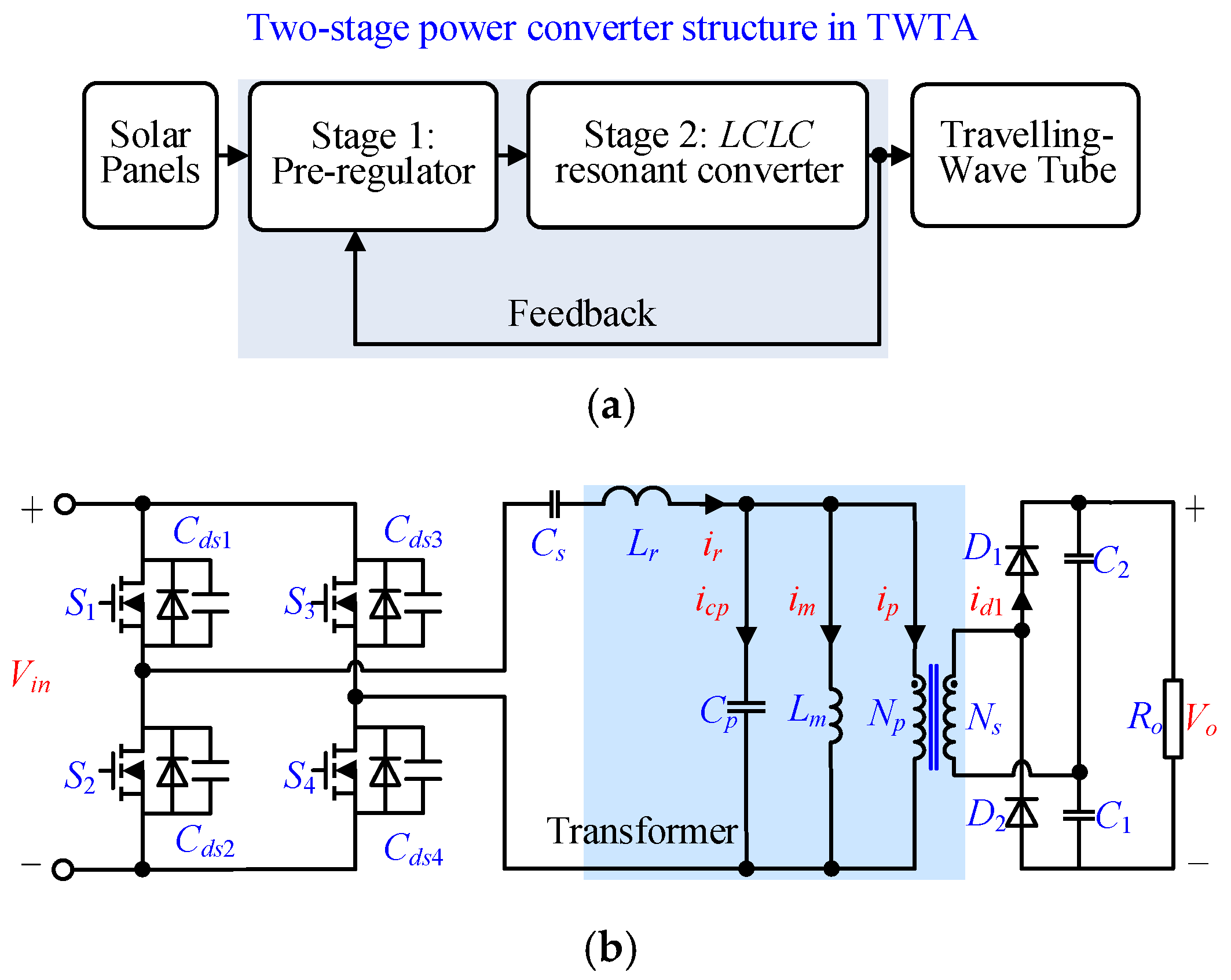
In an electronic power conditioner (EPC) of a space travelling-wave tube amplifier (TWTA), the two-stage power converter structure, as illustrated in Figure 1a, is universally applied; the first stage is a close-loop buck or boost converter, and the second stage is an open-loop LCLC resonant converter, as shown in Figure 1b [1,2]. In the two-stage power converter structure, the output voltage is controlled by the first stage, and the second stage is an unregulated converter whose functions are to boost the input voltage and provide galvanic isolation while keeping high efficiency [1]. Therefore, it is extremely necessary to operate under high efficiency for an LCLC resonant converter [2].
Previous research on LCLC resonant converters can be reviewed as close-loop [3,4,5,6,7,8,9] and open-loop [2,10]. In [3], an extra capacitance was introduced into an LLC resonant tank to build an LCLC resonant tank, and the traditional LLC control method was applied in an LCLC resonant converter. In [4,5], a special closed loop was designed to regulate the voltage-gain of an LCLC resonant converter. In [6], interleaved control was utilized to improve the performance of an LCLC resonant converter at the overload condition. In [7], an LCLC resonant converter control was re-designed for dual outputs. In [8], the closed loop control method of an LCLC resonant converter was investigated for multi-level converters. In [9], a special control method of an LCLC resonant converter was proposed to regulate its input port impedances to realize the maximum power point tracking (MPPT) of the solar panel. Compared to a close-loop LCLC resonant converter, research on the open-loop LCLC resonant converter is rarely reported. Paper [10] investigated the zero-voltage-switching (ZVS) conditions of an open-loop LCLC resonant converter. Paper [2] further analyzed both the ZVS and zero-current-switching (ZCS) conditions of an open-loop LCLC resonant converter, and it also derived analytical equations for an LCLC resonant converter.
Besides the papers reviewed above, there are also other publications on LCLC resonant converters [11,12,13,14,15,16]. In [14], a resonant capacitor was in series with the magnetizing inductance, which aimed at changing the impedance of the magnetizing inductance. However, it should be noted that, although these LCLC resonant converters share the same ‘LCLC’ name, they hold totally different topologies with Figure 1b.
Most of these reviewed papers concentrated on the analysis of topologies [2,10] or the control strategies of LCLC resonant converters [4,5,7,8,9], while rare papers focused on the power loss of an LCLC resonant converter [2,10].
It is known that an open-loop LCLC resonant converter is the first option for the second stage part of a high voltage DC/DC converter in space TWTA applications. As discussed before, most of the existing research of the open-loop LCLC resonant converter were only focused on how to achieve ZCS and ZVS to minimize switching loss [1,2]. However, switching loss is only one part of the total power loss in an LCLC resonant converter. It should be noted that, apart from the switching loss, its total power loss also includes the driving and conduction loss of the main switches, the power loss of the high voltage rectifiers [17], the copper loss of the transformer [18], the core loss of the transformer [19], and the dielectric loss of the transformer [20]. In other words, for an LCLC resonant converter, ZCS and ZVS mean that the switching loss is minimized, but the total power loss of the converter is not. As a result, in order to achieve high efficiency, the total power loss of the converter needs to be further optimized. However, due to the multiple resonant components and their mutual couplings, the optimization of the total power loss is very challenging. As a result, based on the above review, analysis of the optimization of total power loss is rarely reported.
Therefore, aiming to minimizing the total power loss of an LCLC resonant converter, a PSO-algorithm-based, efficiency-oriented optimal design method for an LCLC resonant converter is proposed. In the optimal design method, all the power losses, including the driving and conduction loss of the main switches, the copper loss, core loss, the rectifier loss, and, especially, the dielectric loss of the transformer are considered. At first, the working principles of an LCLC resonant converter are reviewed, and the equations of the main parameters are derived. Secondly, based on working principles and the equations of the main parameters, the total power loss of an LCLC resonant converter is calculated. Thirdly, the total power loss is assigned as the objective function of the PSO algorithm, which then optimizes it. The optimal resonant components, including the leakage inductance (Lr), series resonant capacitance (Cs), parasitic capacitance of the transformer (Cp), and the magnetizing inductance (Lm) are derived. Finally, an LCLC resonant converter with the optimal parameters is built to realize the optimal design.
The rest of this paper is arranged as follows. In Section 2, the working principles and the calculations of the main parameters of an LCLC resonant converter are summarized. In Section 3, the proposed PSO-algorithm-based, efficiency-oriented optimal design method is elaborated upon. At first, based on the equations in Section 2, the total power loss of an LCLC resonant converter is calculated. After that, the total power loss is appointed as the objective function of the PSO algorithm, which then optimizes it. In Section 4, the proposed optimal design method is validated by an example. Section 5 summarizes the whole paper.
2. Review of the Working Principles and the Circuit Analysis of an LCLC Resonant Converter for Space TWTA Applications
2.1. WorkingPrinciples of an LCLC Resonant Converter for Space TWTA Applications
The typical waveforms of an LCLC resonant converter are shown in Figure 2. The main waveforms of interest are listed as follows:
- (a)
- The driving signals of the main switches—vgs1(t), vgs2(t), vgs3(t), and vgs4(t);
- (b)
- the resonant current, ir(t);
- (c)
- the current of Lm, im(t);
- (d)
- the voltage across the series capacitor (Cs), vcs(t);
- (e)
- the voltage across the parasitic capacitor of the transformer Cp, vcp(t);
- (f)
- the voltage across the parasitic capacitor of S1, vds1(t)—same as vds4(t);
- (g)
- the voltage across the rectifier diode D1, vd1(t); and
- (h)
- the current of the rectifier diode D1, id1(t).
Half a period of an LCLC resonant converter can be divided into three modes, and the equivalent circuit in each mode is shown in Figure 3.
Mode 1 (t1, t2): The waveforms of Mode 1 are shown in Figure 2, from t1 to t2, and the equivalent circuit of Mode 1 is illustrated in Figure 3a. Before Mode 1, the voltages of S1 and S4 are zero while the resonant current, ir(t), is also zero. In addition, the voltage of D1 is on, and Cp is clamped by the output voltage. As a result, when S1 and S4 are turned on at t1, both the ZCS and ZVS of S1 and S4 are achieved. Similarly, at t1, as the voltage and current of D1 are also zero, and both the ZCS and ZVS of D1 are achieved.
In Mode 1, the resonance begins between Lr and Cs, and the power is transferred from the primary side to the load. As Cp is clamped, im(t) increases linearly. When ir(t) is equal to im(t), D1 is turned off naturally, Mode 1 ends. As the voltage and current of D1 at t2 reach zero, D1 operates under ZCS and ZVS.
Mode 2 (t2, t3): The waveforms of Mode 2 are shown in Figure 2, from t2 to t3, and the equivalent circuit of Mode 2 is illustrated in Figure 3b. In Mode 2, because D1 is off, Cp is not clamped by the output voltage any more. The resonance begins among Lr, Cs, Lm and Cp. At t3, ir(t) decreases to zero, and S1 and S4 are turned off. As the voltage and current of S1 and S4 are zero, S1 and S4 operate under ZCS and ZVS.
When S1 and S4 are turned off, Mode 2 ends.
Mode 3 (t3, t4): The waveforms of Mode 3 are shown in Figure 2, from t3 to t4, and the equivalent circuit of Mode 3 is illustrated in Figure 3c.
In Mode 3, as all the switches are off, a complex resonance begins among Lr, Cs, Lm, Cp, and all the parasitic capacitances of the switches, including Cds1, Cds2, Cds3, and Cds4. During Mode 3, the voltages of S1 and S4 increase from zero to Vin while the voltages of S2 and S3 decrease from Vin to zero, accordingly. In addition, the voltage of Cp reverse to −aVo/2 (a is the turns ratio of the transformer) and be clamped again. The magnetizing current, im(t), keeps increasing before the voltage of Cp decreases to zero. When the voltage of Cp decreases to zero, the peak value of im(t), Im_pk, occurs.
When the voltages of Cds1 and Cds4 increase to Vin, Mode 3 ends and the other half period begins.
The second half of a period is similar to the first half period, with Mode 4 similar to Mode 1, Mode 5 similar to Mode 2 and Mode 6 similar to Mode 3.
2.2. Derivations of the Eqauitions of the Main Paramters in an LCLC Resonant Converter
The equations of the main parameters are summarized in this part, and they include the voltage gain, the RMS (Root-Mean-Square) value of ir(t), Ir_rms; the peak value of im(t), Im_pk; the RMS value of the current across Cp, Icp_rms; the time for Mode 3, Td; and the switching period, Ts.
The voltage gain of an LCLC resonant converter can be calculated by [2]:
where a is the turns ratio of the transformer.
The RMS value of ir(t) can be calculated by [2]:
where Ro is the load, frs is the resonant frequency between Lr and Cs, and fs is the switching frequency.
The peak value of im(t) can be calculated by [2]:
where frp is the resonant frequency between Lm and Cp.
Based on (3), the corresponding peak magnetic flux density can be calculated by [1,2]:
where Np is the number of turns in the primary winding and Ae is the cross-sectional area of the core.
2.3. Conditions of ZCS and ZVS for LCLC Resonant Converters
As shown in Figure 2, in order to achieve ZVS, enough dead time (Td), must be left for charging Cds1 and Cds4 while discharging Cds2 and Cds3. Therefore,
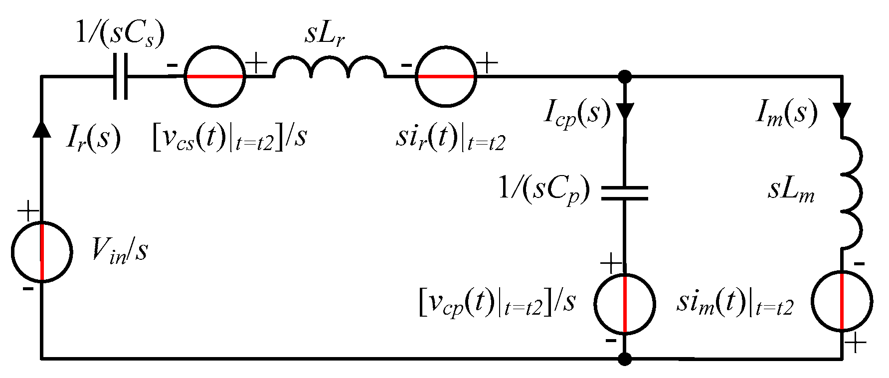
In addition, as the reverse conduction of the antibody diode of the main switch causes extra loss, the circuit design should guarantee that the reverse conduction of the antibody diode of the main switch is avoided. In order to investigate the criterion, Mode 2 was studied. The equivalent circuit of Mode 2 in the s domain is shown in Figure 4.
Based on Figure 4, the following equations can be derived:
The resonant current in the time domain of Mode 2 is:
The minimum value of (10) is utilized as the criterion of ZCS, which can be expressed as:
In the following optimal design method, Equations (8) and (11) are used as the criterions of ZCS and ZVS. However, it is worth noting that with ZCS and ZVS achieved in an LCLC resonant converter, its total power loss (Ptot) still includes the conduction loss of the rectifiers (PD), the driving loss of the main switch (Ps_dr), the conduction loss of the main switch (Ps_on), the copper loss of the transformer (PT_Cu), the core loss of the transformer (PT_Fe), and the dielectric loss of the transformer (PT_Die), which means the total power loss needs further optimization. Therefore, a PSO-algorithm-based, efficiency-oriented optimal design method is proposed, and it is elaborated upon in the following section.
3. Proposed PSO-Algorithm-Based, Efficiency-Oriented Optimal Design Method of an LCLC Resonant Converter for Space TWTA Applications
In this section, a PSO-algorithm-based, efficiency-oriented optimal design method for LCLC resonant converters is proposed. In the first part, based on the working principles and the equations in the previous section, the total power loss of an LCLC resonant converter is calculated. In the second part, the proposed optimal design method is elaborated upon. In the third part, the proposed optimal design method is evaluated by an example.
3.1. Derivation of the Total Power Loss of an LCLC Resonant Converter
In this part, the power losses of an LCLC resonant converter, including the conduction loss of the rectifiers (PD), the driving loss of the main switch (Ps_dr), the conduction loss of the main switch (Ps_on), the copper loss of the transformer (PT_Cu), the core loss of the transformer (PT_Fe), and the dielectric loss of the transformer (PT_Die), are derived.
The conduction loss of the rectifiers can be calculated by:
where Io is the output current and VD is forward voltage of the rectifier diode.
The driving loss of the main switch (Ps_dr) can be calculated by:
where Vgs is the driving voltage, fs is the switching frequency, and Qg is the gate charge.
Based on Equation (2), the conduction loss of the main switch (Ps_on) can be calculated by:
where Vo is the output voltage and Rs_on is the conduction resistance of the switch.
Based on Equation (2), the copper loss of the transformer (PT_Cu) can be calculated by:
where Rac is the AC resistance of the transformer.
Based on Equation (5), the core loss of the transformer (PT_Fe) can be calculated by:
where kc, α, and β, are the parameters of the magnetic material and Ve is the volume of the core.
Based on Equation (6), the dielectric loss of the transformer (PT_Die) is:
where δ is power loss angle, Td is dead time, and ϕ is a constant.
Based on Equations (12)–(17), the total power loss of an LCLC resonant converter can be calculated by:
The above total power loss equation is utilized in the following proposed optimal design method as the objective function.
3.2. Proposed PSO-Algorithm-Based Efficiency-Oriented Optimal Design of an LCLC Resonant Converter
In Equation (18), there are four resonant components to be optimized. In addition, these four resonant components are internally coupled. Furthermore, the conditions of ZCS and ZVS must be satisfied to reduce the switching loss. As a result, due to the above reasons, it may be concluded that the optimal design of an LCLC resonant converter is very challenging. In order to solve this problem, the AI (Artificial Intelligence) algorithm, PSO, is utilized for the optimal design of an LCLC resonant converter.
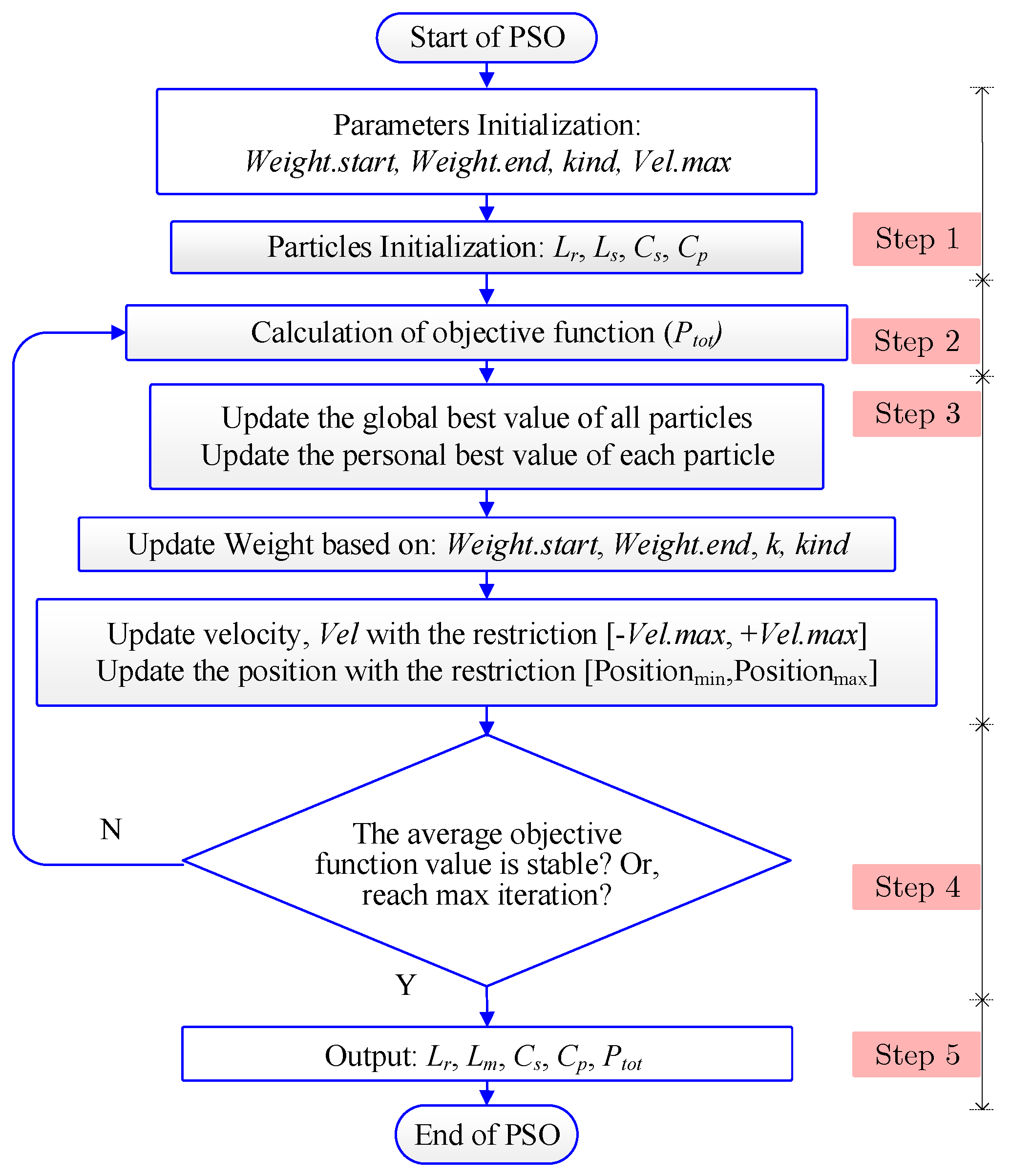
Nowadays, the PSO algorithm is universally applied in the optimal design process because of its internal capability in solving the complicated problems and parallelism [21,22,23]. Furthermore, the population-based method has an excellent performance for global optimization and can deal with objective functions which are linear or nonlinear and continuous or discontinuous. In this paper, the PSO algorithm is used to deal with the difficulties caused by multiple variables and internal couplings of an LCLC resonant converter. The flowchart of the proposed PSO-algorithm-based, efficiency-oriented optimal design of an LCLC resonant converter is shown in Figure 5, and each sequence is explained as follows:
At first, all the parameters—including the parameters of an LCLC resonant converter, Vin, Vo, fs, and Ro; the parameters of the transformer, kc, α, β, Ve, and Rac; the parameter of the insulators for the transformer, tanδ; the parameters of the main switches, Vgs, Qg, and Rs_on; and the parameter of the rectifiers, VD—are input into the optimal design method.
After that, the total power loss, considering the conditions of ZCS and ZVS, is optimized by the PSO algorithm, and the optimal parasitic parameters, Lr, Cs, Lm, Cp, and Ptot, are obtained. The details of the PSO algorithm will be elaborated upon later.
Finally, an LCLC resonant converter with the optimal parameters is realized by proper design.
The PSO algorithm is elaborated upon in the following part.
3.3. PSO Algorithm for the Optimal Design Method
The flowchart of the PSO algorithm is shown in Figure 6 and elaborated on as follows:
Step 1: Initialization of the PSO algorithm
The parameters of the PSO algorithm, including Weight.start, Weight.end, kind, and Vel.max, are initialized. The parameters of the number of the particles, Npa, is 20; the maximum iteration number in PSO, Max.Iteration, is 100.
Each particle is assigned with random Lr, Cs, Lm, and Cp within the given range. The parameters of an LCLC resonant converter are input into PSO. The equation of the total power loss, Equation (18), is assigned as the objective function of the PSO.
Step 2: Calculation of the total power loss (Ptot)
In this step, the objective function of each particle, namely the total power loss, is calculated with Equation (18), which is used to evaluate the fitness value of each particle.
Step 3: Update of global best value, personal best value, Weight and Vel
The global best value of all particles and the personal best value of each particle, Weight and Vel, are updated based on the total power loss and the corresponding restrictions.
Step 4: Repeat of Step 2 and Step 3 until the ending condition is satisfied
In Step 4, if the average objective function value is stable or the Max.Iteration is reached, the recycling process is terminated. Otherwise, Step 2 and Step 3 are repeated.
Step 5: Output the optimal results, including optimal Lr, Cs, Lm, Cp, Ptot
After the recycling process of Step 2 and Step 3 is finished, the optimal Lr, Cs, Lm, Cp, and Ptot, which are the outputs of the PSO algorithm, are obtained.
At this moment, the PSO algorithm comes to the end. After the total power loss is optimized by the PSO algorithm, the optimal Lr, Cs, Lm, Cp, and Ptot are derived. An LCLC resonant converter with optimal parameters could then be built to realize the optimal design results. In the following part, the proposed PSO-algorithm-based, efficiency-oriented optimal design method is evaluated by an example.
3.4. Evaluation of the Proposed PSO-Algorithm-Based, Efficiency-Oriented Optimal Design Method
In this part, the proposed PSO-algorithm-based, efficiency-oriented optimal design method of an LCLC resonant converter is evaluated by an example. The input voltage is 40 V, and the output voltage is 4800 V. The switching frequency is 320 kHz, and the output power is 288 W. Based on the switching frequency and power rating, the magnetic core, FEE 38/16/25 (with N87 from TDK), is selected. In addition, the main switch, RJK 6505PBF, is chosen based on the input voltage and power rating. The parameters of the converter, the magnetic core, and the main switches are listed in Table 1.
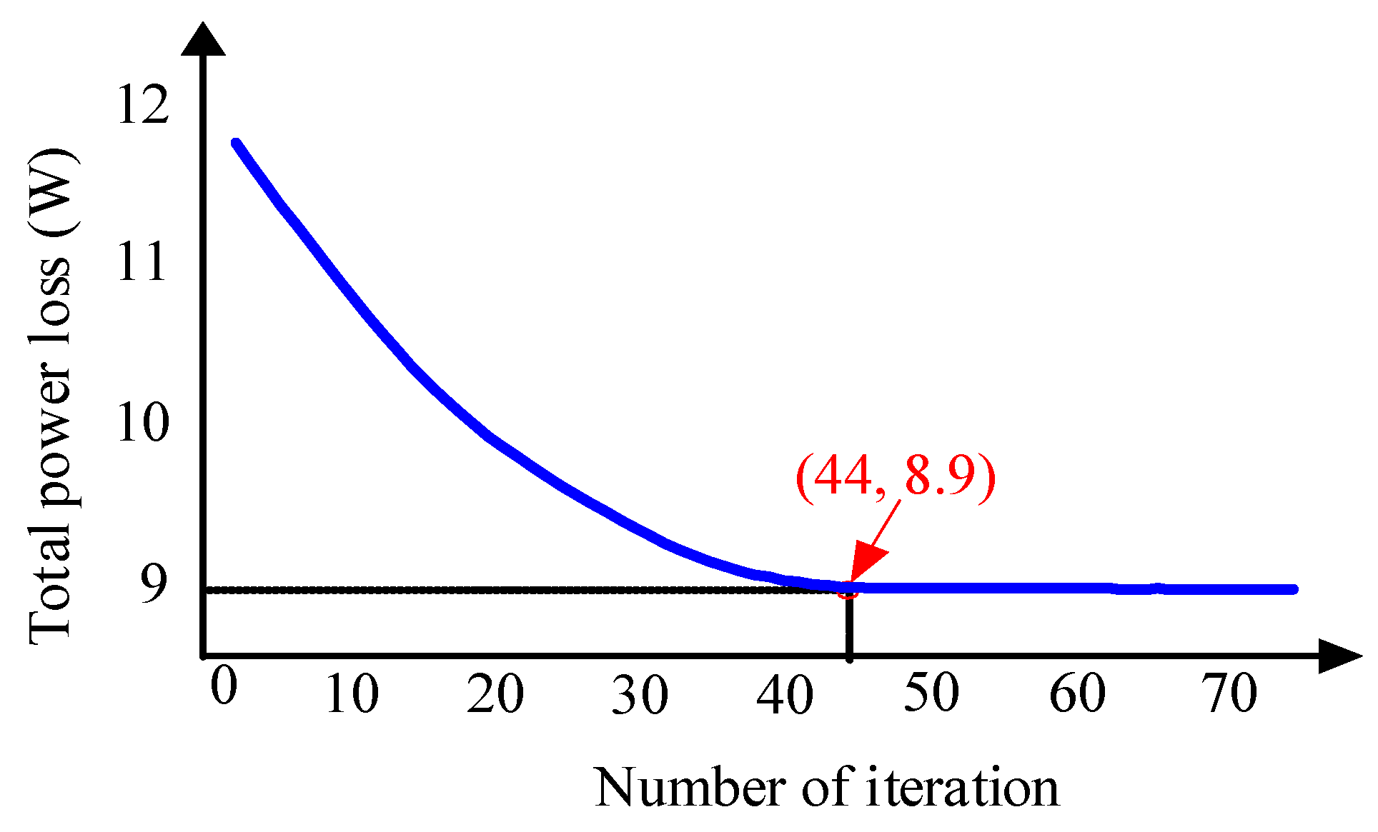
With the parameters shown in Table 1, the total power loss of an LCLC resonant converter is optimized by the PSO algorithm, following the sequences in the previous part. The algorithm is executed in MATLAB on a laptop, and the total execution time is 12.55 s. The variation of the total power loss with the number of iterations is shown in Figure 7. It can be seen from Figure 7 that the total output power becomes stable after several iterations. The final optimized total power loss is 8.9 W.
According to the proposed PSO algorithm, the optimal Lr, Cs, Lm, Cp, and Ptot can be obtained as follows: Lr = 0.09 µH, Cs = 1.0 µF, Lm = 8.0 µH, Cp = 13.2 nF, and Ptot = 8.9 W.
After the optimal design process is finished, an LCLC resonant converter with the optimal design parameters can be designed to realize the optimal design results. In the following section, an optimal LCLC resonant converter is built, and the proposed PSO-algorithm-based, efficiency-oriented optimal design method is validated by the experiments.
4. Experimental Validation
In this section, an LCLC resonant converter with the optimal design parameters obtained in Section 3 is built. An improved partially interleaved transformer structure proposed in [21] was adopted to achieve the optimal leakage inductance, magnetizing inductance, and parasitic capacitance, while an optimal series capacitor (Cs) was designed by selecting the proper capacitance value. After an LCLC resonant converter was built, the effectiveness of the proposed optimal design method was evaluated by changing magnetizing inductance and series capacitance. Finally, the proposed optimal design method was further validated by testing its efficiency under different input voltages and output power.
4.1. Prototype of an LCLC Resonant Converter with Optimal Parameters
With the optimal parameters obtained from the PSO algorithm, the prototype of an LCLC resonant converter was built. Due to the advantages of low leakage inductance, low parasitic capacitance, and low AC resistance, the improved partially interleaved transformer structure presented in [24] was adopted, which is illustrated in Figure 8.
The dimensions of the transformer and the windings for the optimized LCLC resonant converter are shown in Table 2.
Using the dimensions of the transformer shown in Table 2, a 2-D model of the transformer was built in Ansys Maxwell. Hybrid electromagnetic simulations were carried out to simulate the parasitic parameters. The simulated leakage inductance, magnetizing inductance, and parasitic capacitance of the transformer are listed in Table 3. In order to make a comparison, the desired values are listed in Table 3 as well.
It can be seen from Table 3 that the simulated values were in accordance with the desired values, which means that the optimal Lr, Lm and Cp were achieved. For the optimal Cs, since Cs is a detached component, a capacitor with the desired capacitance value was selected.
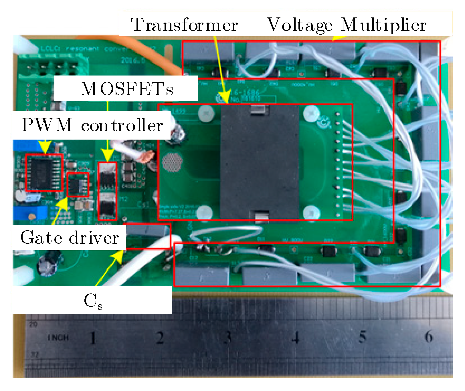
As a result, the LCLC resonant converter with the optimal parameters was built, and it is shown in Figure 9. In the following part, the LCLC resonant converter is tested to evaluate the effectiveness of the proposed optimal design method.
4.2. Evaluation of the Proposed PSO-Algorithm-Based, Efficiency-Oriented Optimal Design Method
The PSO-algorithm-based, efficiency-oriented optimal design method was evaluated with the LCLC resonant converter shown in Figure 9.
The waveforms of the resonant current, ir(t); the voltage of S1, vds1(t); and the driving signals of S1, vgs1(t), are shown in Figure 10a, while the driving signal of S1, vgs1(t); the voltage of D1, vd1(t); and the current of D1, id1(t), are shown in Figure 10b.
It can be seen from Figure 10a that when S1 was turned on, the voltage of S1, vds1(t), and the current of S1, ir(t), were zero. As a result, S1 operated under the ZVS and ZCS (turn-on) condition. In addition, when S1 was turned off, the voltage of S1, vds1(t), and the current of S1, ir(t), were zero. As a result, S1 operated under the ZVS and ZCS (turn-off) condition.
In addition, it can be seen from Figure 10b that when D1 was turned on, the voltage of D1, vd1(t), and the current of D1, id1(t), were zero. As a result, D1 operated under the ZVS and ZCS (turn-on) condition. In addition, when D1 was turned off, the voltage of D1, vd1(t), and the current of D1, id1(t), were zero. As a result, D1 operated under the ZVS and ZCS (turn-off) condition.
Based on the above analysis, it can be concluded that both the main switches and the rectifiers operated under the ZCS and ZVS condition.
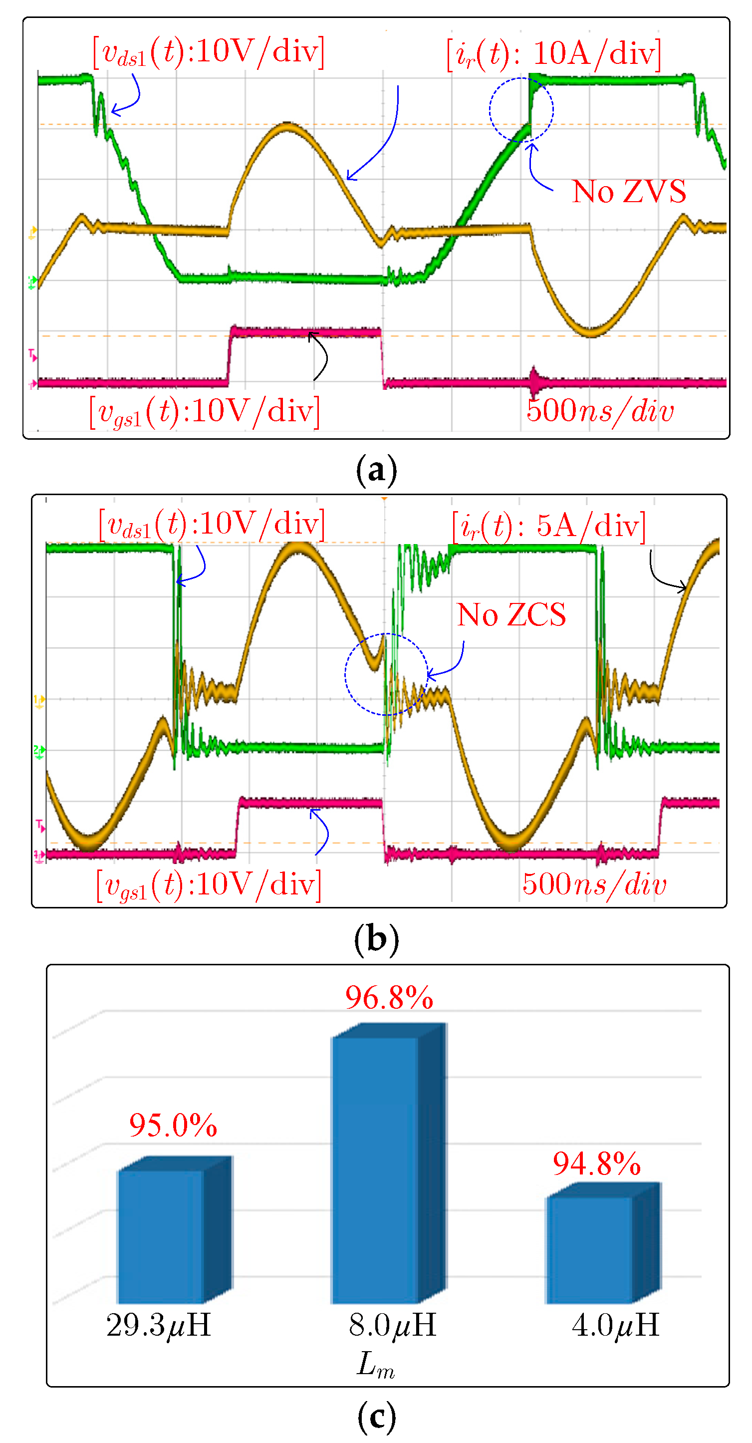
In order to further evaluate the effectiveness of the proposed optimal design method, Lm and Cs were changed to deviate from their corresponding optimal values.
The experimental waveforms with different Lm are shown in Figure 11a,b, while the comparison of the efficiency is shown in Figure 11c.
It can be seen from Figure 11a that when Lm was higher than the optimal value, the ZVS of the main switches was lost, which is shown in Figure 11a. In addition, it can be seen from Figure 11c that the efficiency decreased from 96.8% to 95.0%.
It can be seen from Figure 11b that when Lm was lower than the optimal value, the advantages of ZCS were lost, which are shown in Figure 11b. In addition, it can be seen from Figure 11c that the efficiency decreased from 96.8% to 94.8%.
Based on the experiments with different Lm, it can be concluded that when Lm deviates from the optimal design value, the advantage of ZCS or ZVS may be lost, and the efficiency may decrease as well, which validates the effectiveness of the proposed method.
The experimental waveforms with different Cs are shown in Figure 12a,b, while the comparison of the efficiency is shown in Figure 12c.
It can be seen from Figure 12a that when Cs was lower than the optimal value, the ZVS of the main switches was lost, which is shown in Figure 12a. In addition, it can be seen from Figure 12c that the efficiency decreased from 96.8% to 94.0%.
It can be seen from Figure 12b that when Cs was higher than the optimal value, the advantages of ZCS were lost, which are shown in Figure 12b. In addition, it can be seen from Figure 12c that the efficiency decreased from 96.8% to 95.2%.
Based on the experiments with different Cs, it can be concluded that when Cs deviates from the optimal design value, the advantage of ZCS or ZVS may be lost, and the efficiency may decrease as well, which validates the effectiveness of the proposed method.
Based on the above experiments, it can be concluded that with the PSO-algorithm-based, efficiency-oriented optimal design method, the soft switching of the all the main switches and rectifiers was achieved. In addition, compared with the unoptimized parameters, high efficiency was also achieved.
In space TWTA applications, since the input voltage and the load change, it is necessary to further investigate the performance of the converter under different input voltages and loads.
4.3. Performance of the Optimal LCLC Resonant Converter under Different Input Voltages and Loads
The efficiency under different input voltages is shown in Figure 13a. It can be seen from Figure 13a that at the rated input voltage (40 V), the total measured power loss of the LCLC resonant converter was 9.22 W, while the efficiency was 96.8%. Compared with the result from the PSO-algorithm-based optimal design method, the measured total power loss, which was 9.22 W, is in high accordance with the optimal result of the optimal design methodology, which was 8.9 W.
5. Conclusions
In order to improve the efficiency of an LCLC resonant converter, a PSO-algorithm-based, efficiency-oriented optimal design of an LCLC resonant converter has been proposed.
At first, the working principles of an LCLC resonant converter were reviewed and, based on the working principles, the power losses of each part, including the driving loss, conduction loss, copper loss, core loss, dielectric loss, and the conduction loss of the rectifiers were calculated. Based on the calculated power losses, the total power loss of an LCLC resonant converter was derived. However, due to multiple variables and their internal couplings, the optimization of the total power loss was very challenging.
In this paper, the PSO algorithm was utilized to solve the difficulties caused by the multiple variables, the internal couplings among the variables, and the complicated soft switching conditions. With the total power loss as the objective function, the proposed optimal design method could calculate the optimized total power loss and corresponding optimal parameters of LCLC resonant converters, which can be used to design such a converter.
Finally, the proposed optimal design method was validated by a prototype. In addition, the effectiveness of the optimal design method was been tested by changing the magnetizing inductance and the resonant capacitance.
Author Contributions
Conceptualization, B.Z. and G.W.; Methodology, B.Z.; Software, B.Z.; Validation, B.Z. and G.W.; Formal Analysis, B.Z.; Investigation, B.Z.; Resources, B.Z.; Data Curation, B.Z.; Writing-Original Draft Preparation, B.Z.; Writing-Review & Editing, G.W.; Visualization, G.W.; Supervision, G.W.; Project Administration, G.W.; Funding Acquisition, G.W.
Funding
This research received no external funding.
Conflicts of Interest
The authors declare no conflict of interest.
References
- Barbi, I.; Gules, R. Isolated DC-DC converters with high-output voltage for TWTA telecommunication satellite applications. IEEE Trans. Power Electron. 2003, 18, 975–984. [Google Scholar] [CrossRef] [Green Version]
- Zhao, B.; Wang, G.; Hurley, W.G. Analysis and Performance of LCLC Resonant Converters for High-Voltage High-Frequency Applications. IEEE J. Emerg. Sel. Top. Power Electron. 2017, 5, 1272–1286. [Google Scholar] [CrossRef]
- Lin, R.L.; Huang, L.H. Efficiency Improvement on LLC Resonant Converter Using Integrated LCLC Resonant Transformer. IEEE Trans. Ind. Appl. 2018, 54, 1756–1764. [Google Scholar] [CrossRef]
- Liu, C.; Teng, F.; Hu, C.; Zhang, Z. LCLC resonant converter for multiple lamp operation ballast. In Proceedings of the 2003 Eighteenth Annual IEEE Applied Power Electronics Conference and Exposition, Miami Beach, FL, USA, 9–13 February 2003; pp. 1209–1213. [Google Scholar]
- Williams, D.R.; Foster, M.P.; Bingham, C.M.; Stone, D.A. A genetic algorithm for designing LCLC resonant converters. In Proceedings of the 2008 4th IET Conference on Power Electronics, Machines and Drives, York, UK, 2–4 April 2008; pp. 732–736. [Google Scholar]
- Frivaldsky, M.; Dobrucky, B.; Pridala, M. Analysis of LCLC DC-DC resonant converter in steady state operation. In Proceedings of the IECON 2016—42nd Annual Conference of the IEEE Industrial Electronics Society, Florence, Italy, 24–27 October 2016; pp. 3253–3258. [Google Scholar]
- Bingham, C.M.; Ang, Y.A.; Foster, M.P.; Stone, D.A. Analysis and Control of Dual-Output LCLC Resonant Converters with Significant Leakage Inductance. IEEE Trans. Power Electron. 2008, 23, 1724–1732. [Google Scholar] [CrossRef]
- Kim, E.S.; Lee, H.K.; Kong, Y.S.; Kim, Y.H. Operating Characteristics in LCLC Resonant Converter with A Low Coupling Transformer. In Proceedings of the APEC 07—Twenty-Second Annual IEEE Applied Power Electronics Conference and Exposition, Anaheim, CA, USA, 25 February–1 March 2007; pp. 1651–1656. [Google Scholar]
- Conesa, A.; Velasco, G.; Martinez, H.; Roman, M. LCLC resonant converter as maximum power point tracker in PV systems. In Proceedings of the 2009 13th European Conference on Power Electronics and Applications, Barcelona, Spain, 8–10 September 2009; pp. 1–9. [Google Scholar]
- Shafiei, N.; Pahlevaninezhad, M.; Farzanehfard, H.; Motahari, S.R. Analysis and Implementation of a Fixed-Frequency LCLC Resonant Converter with Capacitive Output Filter. IEEE Trans. Ind. Electron. 2011, 58, 4773–4782. [Google Scholar] [CrossRef]
- Chen, Y.; Wang, H.; Hu, Z.; Liu, Y.F.; Afsharian, J.; Yang, Z.A. LCLC resonant converter for hold up mode operation. In Proceedings of the 2015 IEEE Energy Conversion Congress and Exposition (ECCE), Montreal, QC, Canada, 20–24 September 2015; pp. 556–562. [Google Scholar]
- Nam, I.; Dougal, R.; Santi, E. Optimal design method for series LCLC resonant converter based on analytical solutions for voltage gain resonant peaks. In Proceedings of the 2013 Twenty-Eighth Annual IEEE Applied Power Electronics Conference and Exposition (APEC), Long Beach, CA, USA, 17–21 March 2013; pp. 1429–1437. [Google Scholar]
- Nam, I.; Dougal, R.; Santi, E. Novel control approach to achieving efficient wireless battery charging for portable electronic devices. In Proceedings of the 2012 IEEE Energy Conversion Congress and Exposition (ECCE), Raleigh, NC, USA, 15–20 September 2012; pp. 2482–2491. [Google Scholar]
- Sheng, B.; Chen, Y.; Wang, H.; Liu, Y.; Sen, P.C. High Efficiency Wide Input Voltage Range LCLC Resonant Converter Using Nonlinear Frequency Controller. In Proceedings of the 2018 IEEE Energy Conversion Congress and Exposition (ECCE), Portland, OR, USA, 23–27 September 2018; pp. 1435–1441. [Google Scholar]
- Montoya, F.G.; Alcayde, A.; Arrabal-Campos, F.M.; Baños, R. Quadrature Current Compensation in Non-Sinusoidal Circuits Using Geometric Algebra, Evolutionary Algorithms. Energies 2019, 12, 692. [Google Scholar] [CrossRef]
- Zeng, J.; Qiao, W.; Qu, L. An Isolated Three-Port Bidirectional DC–DC Converter for Photovoltaic Systems with Energy Storage. IEEE Trans. Ind. Appl. 2015, 51, 3493–3503. [Google Scholar] [CrossRef]
- Park, S.; Rivas-Davila, J. Power loss of GaN transistor reverse diodes in a high frequency high voltage resonant rectifier. In Proceedings of the 2017 IEEE Applied Power Electronics Conference and Exposition (APEC), Tampa, FL, USA, 26–30 March 2017; pp. 1942–1945. [Google Scholar]
- Lopera, J.M.; Prieto, M.J.; Díaz, J.; García, J. A Mathematical Expression to Determine Copper Losses in Switching-Mode Power Supplies Transformers Including Geometry and Frequency Effects. IEEE Trans. Power Electron. 2015, 30, 2219–2231. [Google Scholar] [CrossRef]
- Sibue, J.R.; Meunier, G.; Ferrieux, J.P.; Roudet, J.; Periot, R. Modeling and Computation of Losses in Conductors and Magnetic Cores of a Large Air Gap Transformer Dedicated to Contactless Energy Transfer. IEEE Trans. Magn. 2013, 49, 586–590. [Google Scholar] [CrossRef]
- Hao, J.; Fu, J.; Ma, Z.; Zhang, S.; Shen, S. Condition assessment of main insulation in transformer by dielectric loss data interpolation method and database building. In Proceedings of the 2014 International Symposium on Electrical Insulating Materials, Niigata, Japan, 1–5 June 2014; pp. 152–155. [Google Scholar]
- Veerachary, M.; Saxena, A.R. Optimized Power Stage Design of Low Source Current Ripple Fourth-Order Boost DC–DC Converter: A PSO Approach. IEEE Trans. Ind. Electron. 2015, 62, 1491–1502. [Google Scholar] [CrossRef]
- Shi, H.; Wen, H.; Hu, Y.; Jiang, L. Reactive Power Minimization in Bidirectional DC–DC Converters Using a Unified-Phasor-Based Particle Swarm Optimization. IEEE Trans. Power Electron. 2018, 33, 10990–11006. [Google Scholar] [CrossRef]
- de León-Aldaco, S.E.; Calleja, H.; Alquicira, J.A. Metaheuristic Optimization Methods Applied to Power Converters: A Review. IEEE Trans. Power Electron. 2015, 30, 6791–6803. [Google Scholar] [CrossRef]
- Zhao, B.; Ouyang, Z.; Duffy, M.; Andersen, M.A.E.; Hurley, W.G. An Improved Partially Interleaved Transformer Structure for High-voltage High-frequency Multiple-output Applications. IEEE Trans. Ind. Electron. 2018, 66, 2691–2702. [Google Scholar] [CrossRef]
Figure 1.
Typical power supply in a travelling-wave tube amplifier (TWTA): (a) Two-stage power converter structure; (b) an LCLC resonant converter.
Figure 1.
Typical power supply in a travelling-wave tube amplifier (TWTA): (a) Two-stage power converter structure; (b) an LCLC resonant converter.

Figure 2.
Typical waveforms of an LCLC resonant converter.

Figure 3.
Equivalent circuit in each mode: (a) Mode 1; (b) Mode 2; (c) Mode 3.

Figure 4.
Equivalent circuit of Mode 2 in the s domain.

Figure 5.
Flowchart of the PSO-algorithm-based, efficiency-oriented optimal design of an LCLC resonant converter.
Figure 5.
Flowchart of the PSO-algorithm-based, efficiency-oriented optimal design of an LCLC resonant converter.

Figure 6.
Flowchart of the PSO algorithm for an LCLC resonant converter.

Figure 7.
Variation of the total power loss with the number of iterations.

Figure 8.
The improved partially interleaved transformer structure for the optimized LCLC resonant converter.
Figure 8.
The improved partially interleaved transformer structure for the optimized LCLC resonant converter.

Figure 9.
The prototype of the LCLC resonant converter with optimal parameters.

Figure 10.
Experimental waveforms: (a) S1; (b) D1.

Figure 11.
Experimental results with different Lm: (a) Lm = 29.3 µH and (b) Lm = 4.0 µH. (c) Comparison of the efficiency.
Figure 11.
Experimental results with different Lm: (a) Lm = 29.3 µH and (b) Lm = 4.0 µH. (c) Comparison of the efficiency.

Figure 12.
Experimental results with different Cs: (a) Cs = 0.3 µF and (b) Cs = 1.6 µF. (c) Comparison of the efficiency.
Figure 12.
Experimental results with different Cs: (a) Cs = 0.3 µF and (b) Cs = 1.6 µF. (c) Comparison of the efficiency.

Figure 13.
Efficiency under different: (a) Input voltages; (b) loads.


Table 1.
The example LCLC resonant converter whose parameters need to be optimized for the test.
| Parameters | Value | Parameters | Value |
|---|---|---|---|
| Vin | 40.0 V | Ve | 10,200 mm3 |
| Vo | 4800 V | Ae | 190 mm2 |
| fs | 320 kHz | kc | 3.716 × 10⁻²⁴ |
| Ro | 80 kΩ | α | 4.823 |
| Po | 288 W | β | 5.521 |
| Vgs | 10.0 V | Ron | 4.5 mΩ |
| Qg | 40 nC | Rac | 20.0 mΩ |
| Coss | 660 pF |
Table 2.
Dimensions of the transformer and the windings.
| Parameters | Description | Values |
|---|---|---|
| dps | The distance between primary and secondary winding | 0.13 mm |
| dpt | The thickness of the primary winding | 0.2 mm |
| dst | The thickness of the secondary winding | 70 µm |
| da | The thickness of the air gap | 63 µm |
| dpw | The width of the primary winding | 9.6 mm |
| dsw | The width of the secondary winding | 0.28 mm |
| dti | The thickness of the thicker insulation | 1.6 mm |
| dni | The thickness of the normal insulation | 0.3 mm |
Table 3.
Comparison between the simulated values and desired values.
| Parameters | Simulated Values | Desired Values |
|---|---|---|
| Lr | 0.09 µH | 0.09 µH |
| Lm | 8.1 µH | 8.0 µH |
| Cp | 13.0 nF | 13.2 nF |
© 2019 by the authors. Licensee MDPI, Basel, Switzerland. This article is an open access article distributed under the terms and conditions of the Creative Commons Attribution (CC BY) license (http://creativecommons.org/licenses/by/4.0/).
Share and Cite
MDPI and ACS Style
Zhao, B.; Wang, G. PSO-Algorithm-Based Optimal Design of LCLC Resonant Converters for Space Travelling-Wave Tube Amplifiers Applications. Energies 2019, 12, 2444. https://0-doi-org.brum.beds.ac.uk/10.3390/en12122444
AMA Style
Zhao B, Wang G. PSO-Algorithm-Based Optimal Design of LCLC Resonant Converters for Space Travelling-Wave Tube Amplifiers Applications. Energies. 2019; 12(12):2444. https://0-doi-org.brum.beds.ac.uk/10.3390/en12122444
Chicago/Turabian StyleZhao, Bin, and Gang Wang. 2019. "PSO-Algorithm-Based Optimal Design of LCLC Resonant Converters for Space Travelling-Wave Tube Amplifiers Applications" Energies 12, no. 12: 2444. https://0-doi-org.brum.beds.ac.uk/10.3390/en12122444
Note that from the first issue of 2016, this journal uses article numbers instead of page numbers. See further details here.