1. Introduction
Renewable energy applications, such as solar and fuel cell-based energy generation systems produce low DC voltage that has to be stepped up significantly to match the grid level. To meet the challenge, a number of high gain converters were developed and reported in recent literature. Tapped Inductor (TI) converters are a well-known class of converters and are quite popular for renewable energy applications that use a coupled magnetic device with several but, in most cases, just two windings [
1,
2,
3] to attain higher gain. As compared to their uncoupled counterparts TI converters can attain wider conversion ratio by a proper choice of the turn ratio and winding polarity. Yet, this desirable feature comes at a price of pulsating currents and higher voltage stress. The switch voltage stress in TI converters is further aggravated by the leakage inductance discharge. To lower the voltage spike across the semiconductors as well as increase the efficiency of the power stage, the clamp and snubber circuits have to be employed to capture the leakage energy [
3,
4,
5]. Snubbers, however, usually have a limited performance envelope, affect the converter’s conversion ratio, and complicate the converter’s design.
An alternative solution to attaining a wider conversion ratio is using the switched inductor (SI) and switched capacitor (SC) cells [
6,
7,
8]. SI converters can achieve moderately wider conversion ratio and may have an advantage over the TI converters with similar specifications. The key benefit of the SI cells is that they are free from problems associated with the leakage inductance. Therefore, SI converters exhibit lower voltage stress and may need no snubbers [
9,
10,
11]. The increasing popularity of the SI converters can also be attributed to their simplicity, robustness, and modest cost. For these reasons, SI converters became particularly popular in the field of alternative and renewable energy power generation, such as PV applications [
12,
13,
14,
15].
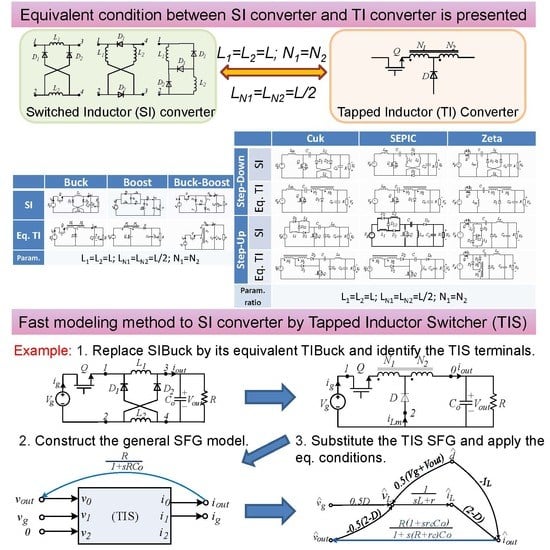
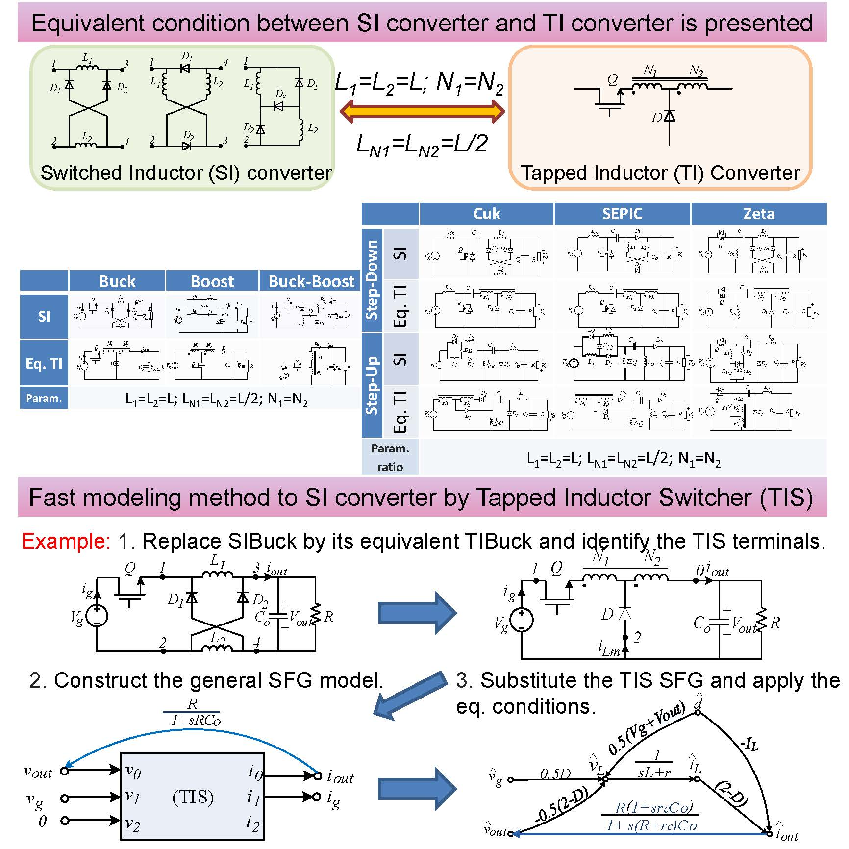
As shown in
Figure 1, switched inductor cells consist of two inductors and multiple diodes. The large component count and switching action may bring complications to analysis and modeling. State space averaging (SSA) [
16] was one of the most popular modeling techniques for switching converters, which can also be employed to analyze SI converters [
15]. However, for more complicated topologies, such as multiple SI cells [
17], extended SI cells with switched capacitor [
12], hybrid SI cells [
18], complicated and tedious formula derivations were required when using the SSA method. An attempt to derive the equivalent circuit model of SI cell has been reported in [
19], however it only discussed the circuit model to the proposed topology. A unified equivalent circuit model of a hybrid type SI cell was proposed in [
20]. The method may cover a wide range of converters but cannot be used for traditional SI cell converters.
Recently an equivalence in between SI Boost and TI Boost converters was suggested [
21]. As reported, under equivalence conditions the ideal SI Boost and its ideal equivalent TI Boost converter are functionally identical as far as their terminal voltages and currents as well as conversion ratio are concerned. The equivalence holds in both continuous and discontinuous modes. Moreover, the equivalent converters have identical frequency responses. This implies that their dynamic models are also identical.
While in [
21] a step-up SI cell was examined, in this paper, with the aim to extend the method further, the step-down SI cell is investigated. Here, the equivalence existing between a number of additional SI converters and their candidate TI equivalent counterparts is revealed. The paper also offers small signal modeling approach of SI converters that can be accomplished in two easy steps. First, the problem SI converter is examined, and its equivalent TI topology is found. Then, taking the advantage of the equivalence feature, the Tapped Inductor Switcher (TIS) model [
22] is applied to the equivalent TI topology. This yields the desired dynamic model of the SI converter.
This paper is organized as follows. Firstly, three basic types of SI cells are reviewed. Then the equivalence conditions of SI Buck, SI Buck-Boost, and SI Boost with their Tapped Inductor counterpart are presented. According to the proposed equivalence methodology, high order hybrid converters with SI cells and their equivalent tapped-inductor converters are discussed in
Section 6. Based on the equivalence between SI converters and TI converters, the unified tapped inductor switcher modeling method (TIS) is studied in
Section 7. As an application example, the small-signal model of the SI Buck converters is derived. The analysis results are confirmed by simulation and experiment.
2. Brief Review of the Switched Inductor Cells
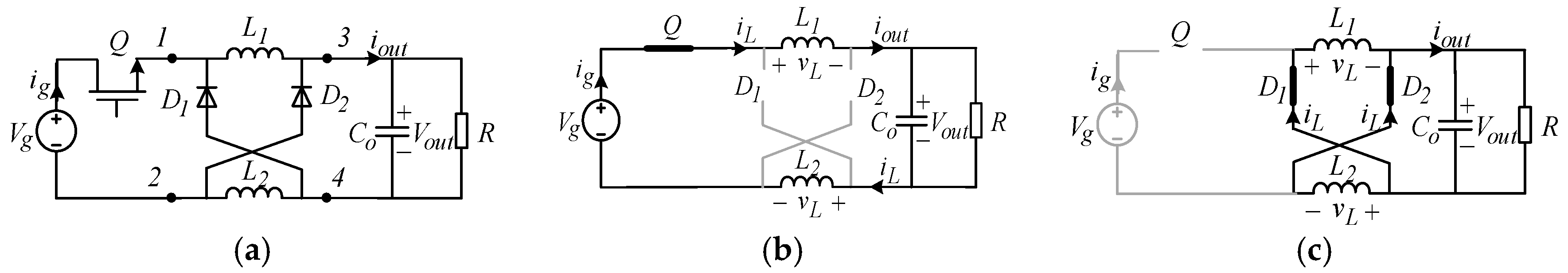
The SI cells, illustrated in
Figure 1, are comprised of a pair of equal valued inductors and a passive (diode only) switching network [
6]. Such SI cells can be used as building blocks of various step-up and step-down dc-dc converters. An SI variant converter can be derived from its traditional counterpart by replacing the regular inductor by the switched inductor cell. The SI cells in
Figure 1a,b can be used in step-down topologies, whereas SI cell in
Figure 1c can provide step-up action.
The SI step-up cell in
Figure 1c has just one pair of terminals. Hence, the SI step-up cell can point-by-point replace an ordinary inductor and readily modify a step-up converter. However, the SI step-down cells in
Figure 1a,b are two-port networks that have to be installed on both the feed and return lines. The latter, however, keeps the output floating.
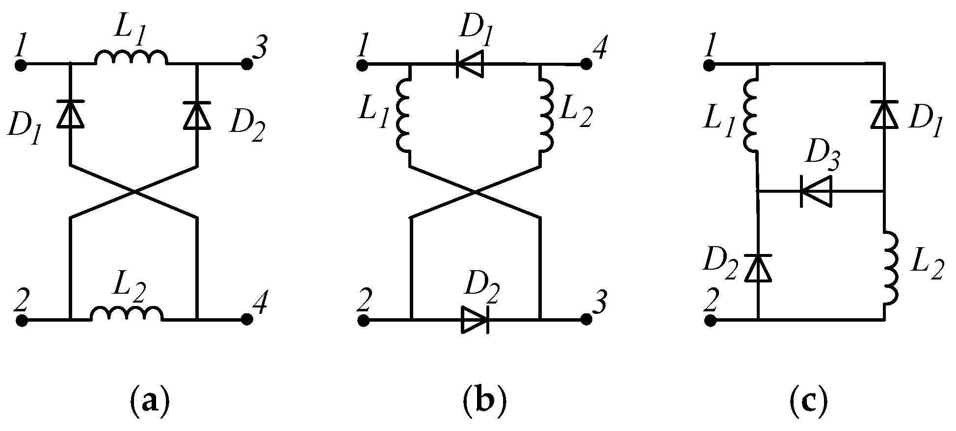
Moreover, taking a closer look at
Figure 1a and unfolding the twisted wiring reveals that the circuit can be redrawn similarly to an H bridge as shown in
Figure 2. The same drill can be repeated in
Figure 1b, which leads to the same
Figure 2. Here it becomes obvious that the circuits in
Figure 1a,b differ only in the designation of the output (load) terminals. That is, except for the polarity of the output voltage, both cells are identical. Since the polarity of the output voltage is merely a matter of convention, such a minor difference is immaterial. Therefore, in the following, only the SI step-down cell in
Figure 2 is considered.
3. Equivalence of the SI Buck and TI Buck Converters
3.1. Review of the SI Buck Converter
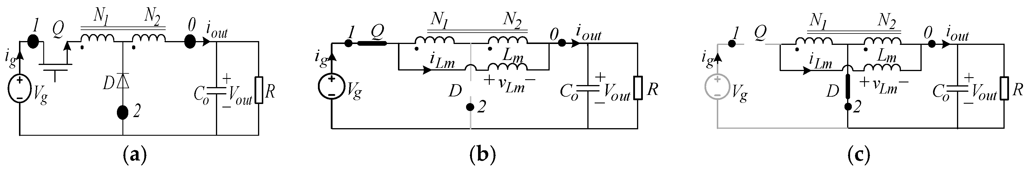
The Switched Inductor Buck (SIBk) converter can be derived off the traditional Buck by imbedding the SI cells as suggested in
Figure 3a. The resulting SIBk is a single switch, simple, and rugged topology. As already mentioned, SI Buck can achieve a steeper conversion ratio than the traditional Buck converter and operate in a wider duty cycle range.
In the following it is assumed that SI Buck in
Figure 3a is comprised of ideal components, i.e., the switches have zero switch-on resistance and no forward voltage drop, and the inductors have zero resistance. It is also assumed that the converter operates in CCM (Current Continuous Mode), so that its switching cycle is comprised of only two intervals: the “on” interval and the “off” interval.
When the active switch in the SI Buck converter is on, a positive voltage,
Vg, is applied to the cell’s input terminals 1 and 2 (see
Figure 3b); the diodes are switched off forcing the inductors to assume series configuration and charge up. Since SI cell is comprised of equally sized inductors,
, the equivalent “on” state inductance of the SI Buck (see
Figure 3b) is
When the active switch is turned off, the diodes turn on to freewheel the inductors’ currents as shown in
Figure 3c with both inductors discharging in parallel to the output. Hence, it is evident (see
Figure 3c) that the equivalent “off state” inductance of the SI Buck is
3.2. Review of the TI Buck Converter
The topology shown in
Figure 4a can be classified as diode-to-tap Tapped Inductor Buck converter with cumulative windings. Henceforth, the topology in
Figure 4a is referred to as the TI Buck (TIBk) converter.
In the following it is assumed that the candidate TIBk converter is ideal (i.e., lossless switches and the ideal tapped inductor with neither leakage nor resistance).
During the “on” interval (see
Figure 4b), the tapped inductor charges through a series cumulative connection of both the primary,
N1, and secondary,
N2, windings having the equivalent inductance of
Here, the magnetizing inductance,
Lm, is defined as the combined inductance of both
N1 and
N2 windings (see
Figure 4).
During the “off” interval (see
Figure 4c), the active switch is turned off while the diode freewheels the magnetizing current to the output through the
N1 winding. Thus, through the autotransformer action of the tapped inductor, the equivalent inductance is
Here is the TI’s turn ratio.
3.3. Derivation of the SIBk and TIBk Equivalence Conditions
The hypothesis proposed herein is that if the parameters of the TIBk converter are adjusted to fulfill the following constraints: and , the resulting TIBk converter can precisely imitate the function of SIBk converter and, thus, can be considered as a functional equivalent (with the exception of different voltage stress across the switches).
Therefore, the necessary equivalence conditions between SIBk and TIBk converters can be obtained equating Equations (1) to (3) and (2) to (4). This yields the following:
In other words, the tapped inductor of the equivalent TIBk converter should have an equal turn winding arrangement, which inductances relate to its SI counterpart according to:
Moreover, since SIBk inductances are equally valued, compared with
Figure 3b,c and
Figure 4b,c, it is evident that, under the equivalence conditions, the TIBk’s magnetizing inductance voltage and current are related to SIBk’s inductors’ voltage and current by
3.4. Comparison of the SIBk and TIBk Simulation Results
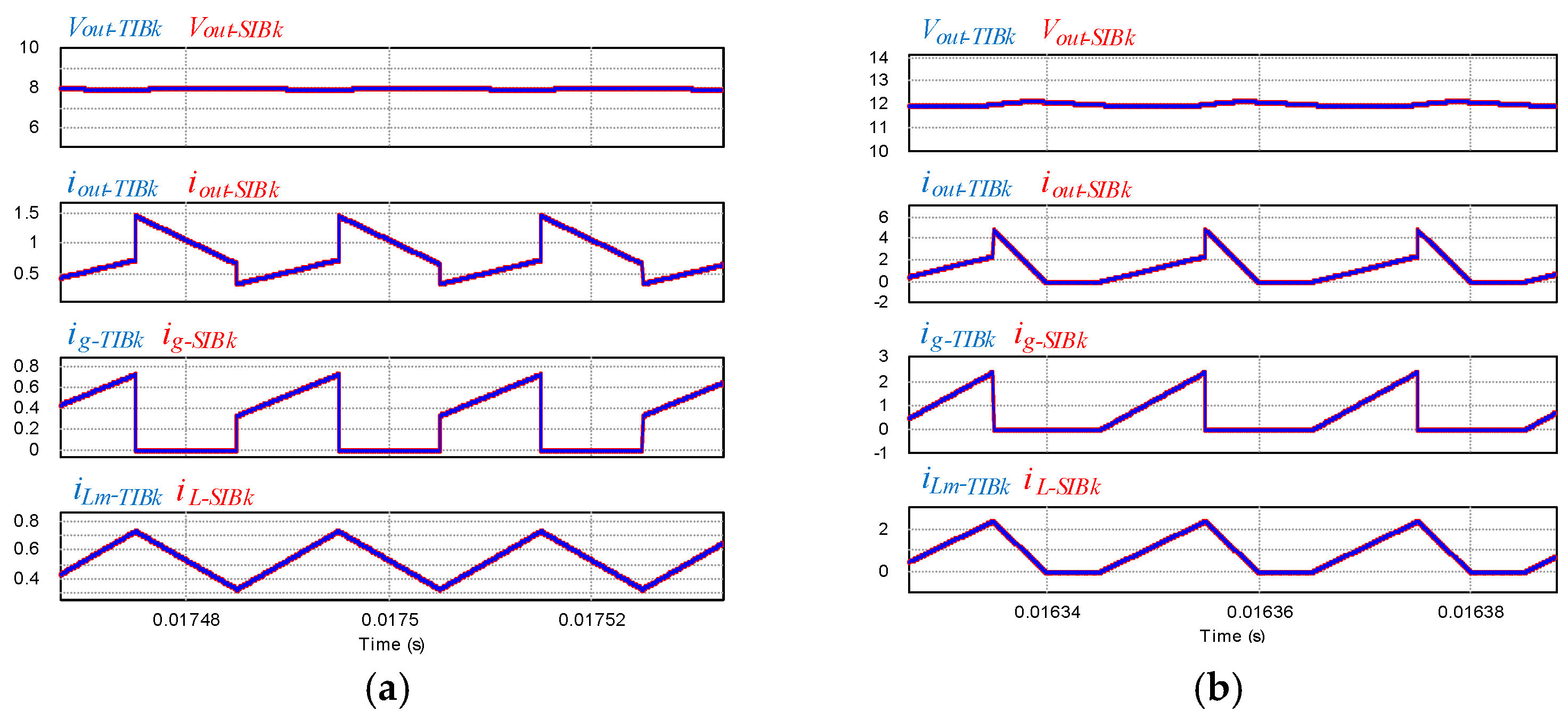
To verify the hypothesis above, benchmark SIBk and its equivalent TIBk were simulated in time domain by PSIM 9.1.4. Both converters were operated with identical duty cycle, D, and had identical filter capacitor Co; identical load R; as well as identical input voltage, Vg. Since this paper aims to study small-signal behavior of SI converters, which have no leakage, the leakage inductance in its TI counterpart is not considered. For this reason, the tapped inductor was simulated by the ideal transformer model in parallel with magnetizing inductance.
The parameters of the benchmark SIBk converter were at CCM and at discontinuous conduction mode (DCM),, D = 0.5, R = 10 Ohm, Co = 47 μF, fS = 50 kHz. The equivalent TIBk converter parameters calculated by Equations (5) and (6) were and for CCM and for DCM. Zero leakage inductance was assumed.
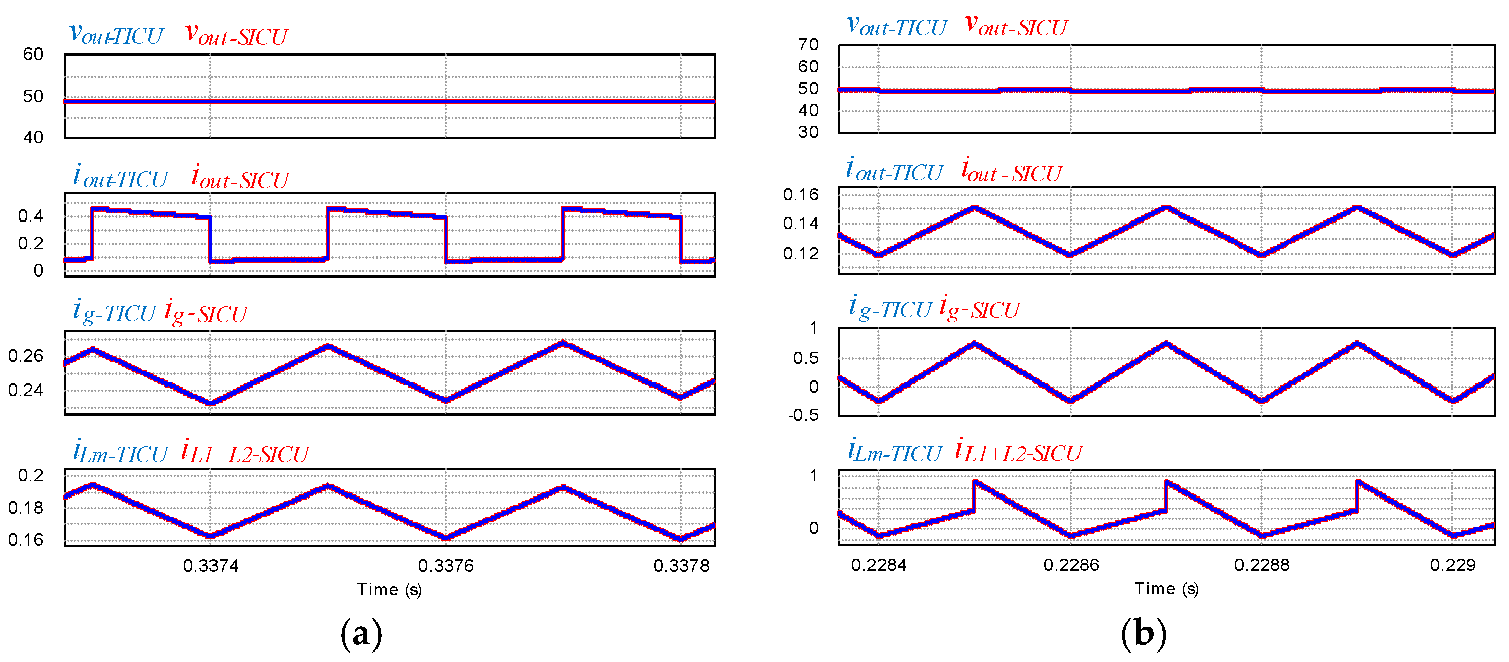
Comparison of key simulated waveforms of both converters in the CCM mode is shown in
Figure 5a, whereas the DCM waveforms comparison is presented in
Figure 5b. In both cases the simulated responses of both SIBk and its equivalent TIBk converters were found to be precisely identical.
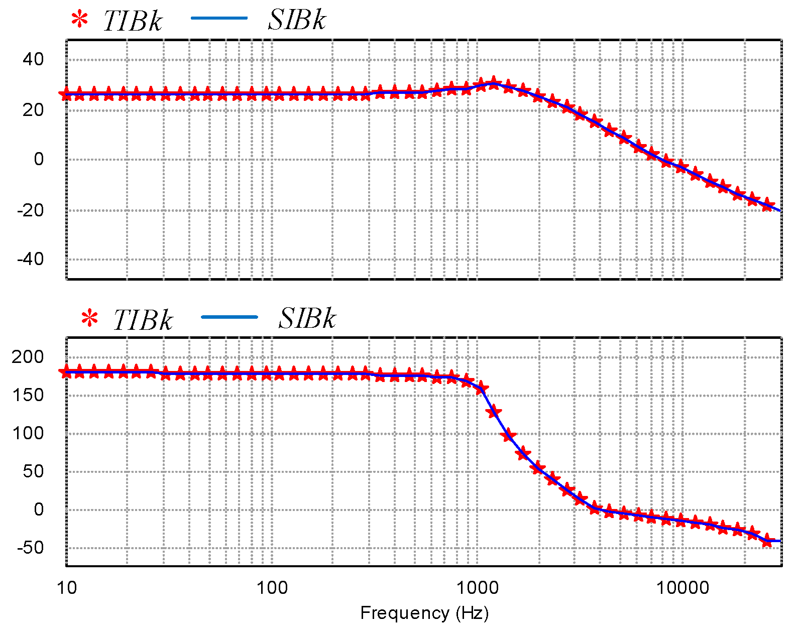
The frequency response of the ideal SIBk and that of its equivalent ideal TIBk converters was compared and is plotted in
Figure 6. As expected, the results are precisely matched. Thus, the notion of the equivalence of SIBk and TIBk converters is confirmed.
4. Equivalence of The SI Buck-Boost and TI Buck-Boost Converters
4.1. Preliminary Considerations and Basic Assumptions
Both the step-down cells in
Figure 1a,b seem incompatible with the Buck-Boost converter. However, by imbedding the step-up SI cell in
Figure 1c into the traditional Buck-Boost topology, the Switched Inductor Buck-Boost (SIBB) converter can be derived as shown in
Figure 7a [
6].
The same as above, it is assumed here that SIBB is made of ideal and lossless components, operates in CCM, and its inductors are identical, that is .
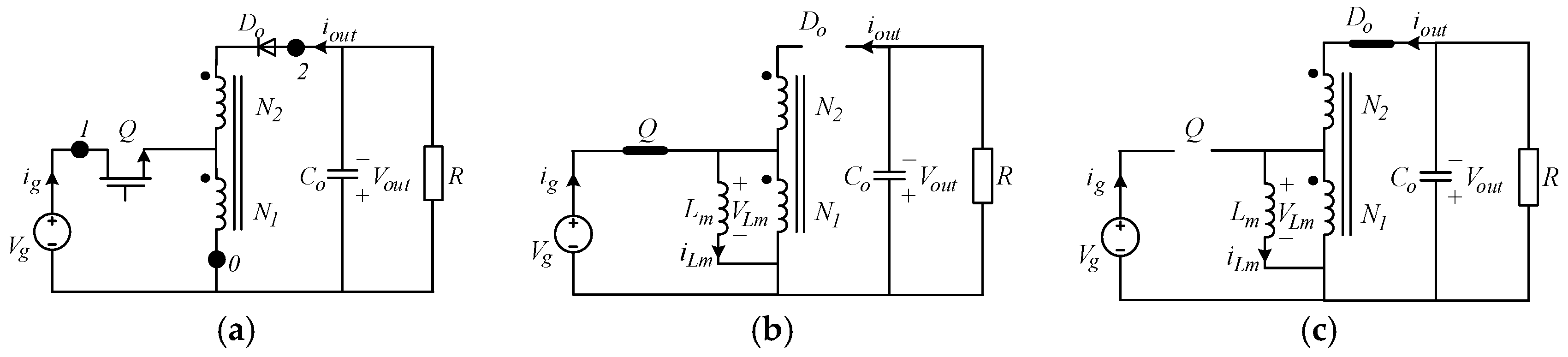
4.2. Review of the SIBB Converter
Examining the SIBBs on state equivalent circuit in
Figure 7b reveals that the equivalent on state inductance seen between the input and the switch terminals is
Whereas during the off interval, the off inductance of the SI Buck-Boost seen between the input and output terminals (see
Figure 1c) is
4.3. Review of the TIBB Converter
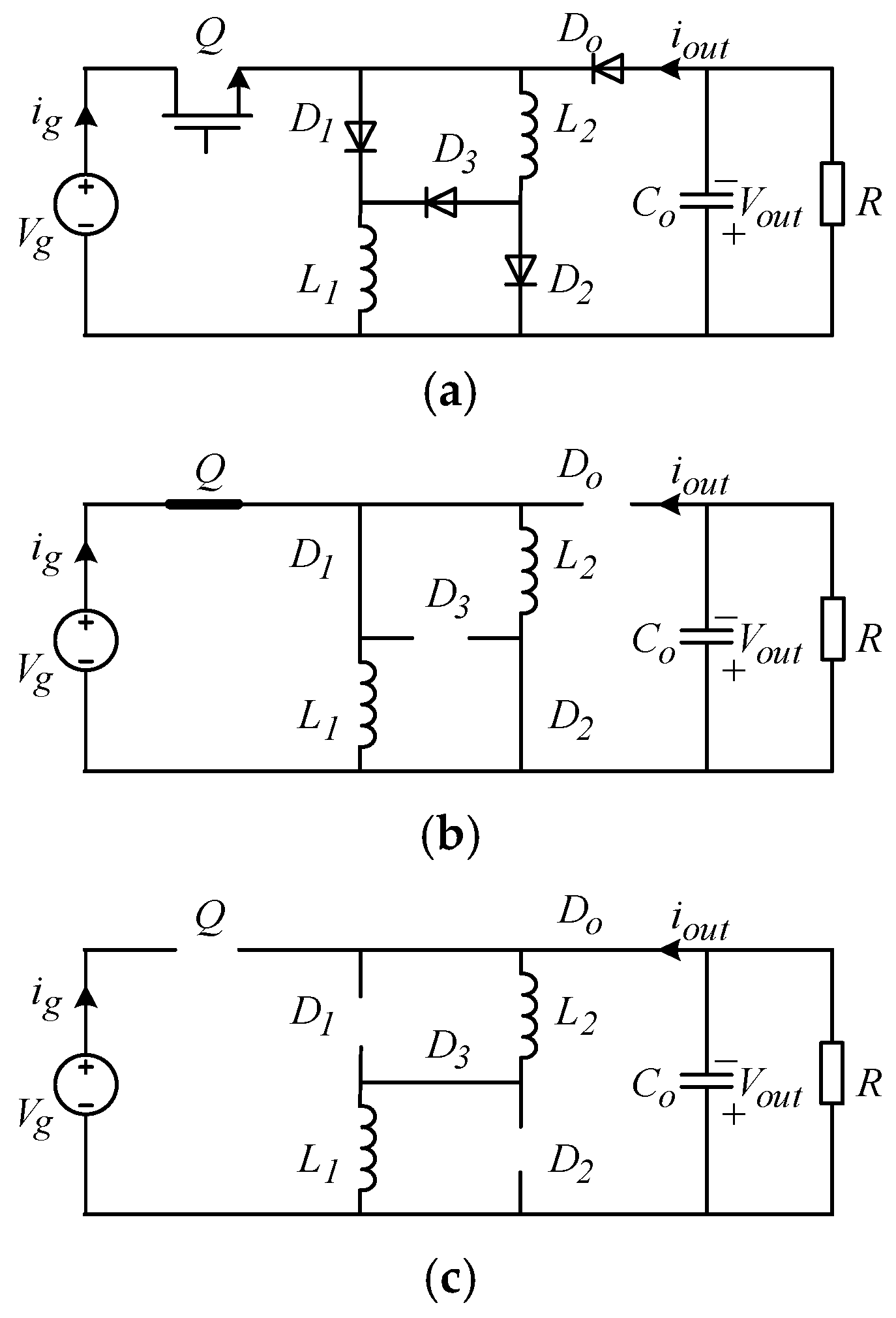
The candidate equivalent Tapped-Inductor Buck-Boost topology (TIBB) is shown in
Figure 8a and can be classified as switch-to-tap TI converter with cumulative windings.
In the following, an ideal TIBB (i.e., lossless switches and the ideal tapped inductor with negligible leakage) which operates in CCM is considered.
During the on interval (see
Figure 8b) the active switch energizes only the N
1 winding. Thus, equivalent inductance seen between the input and the switch terminals (0, 1) is
where the magnetizing inductance,
Lm, is referred to as the N
1 winding as shown in
Figure 8b.
During the “off” interval (see
Figure 8c), the active switch is turned off while the diode freewheels the magnetizing current to the output through both the primary
N1, and the secondary
N2 windings. Thus, through the autotransformer action of the tapped inductor, the equivalent inductance seen between the terminals (0, 2) is
Here, is the turn ratio.
4.4. Derivation of the SIBB and TIBB Equivalence Conditions
Equivalence conditions between SIBB and TIBB converters can be derived equating Equations (12) to (10) and (13) to (11) yielding
Hence, regardless of the definition of the magnetizing inductance, the ratio of self-inductances of the tapped inductor of the equivalent TIBB can be derived by Equation (14) which is same as described by Equation (7).
4.5. Comparison of the SI Buck-Boost and TI Buck-Boost Simulation Results
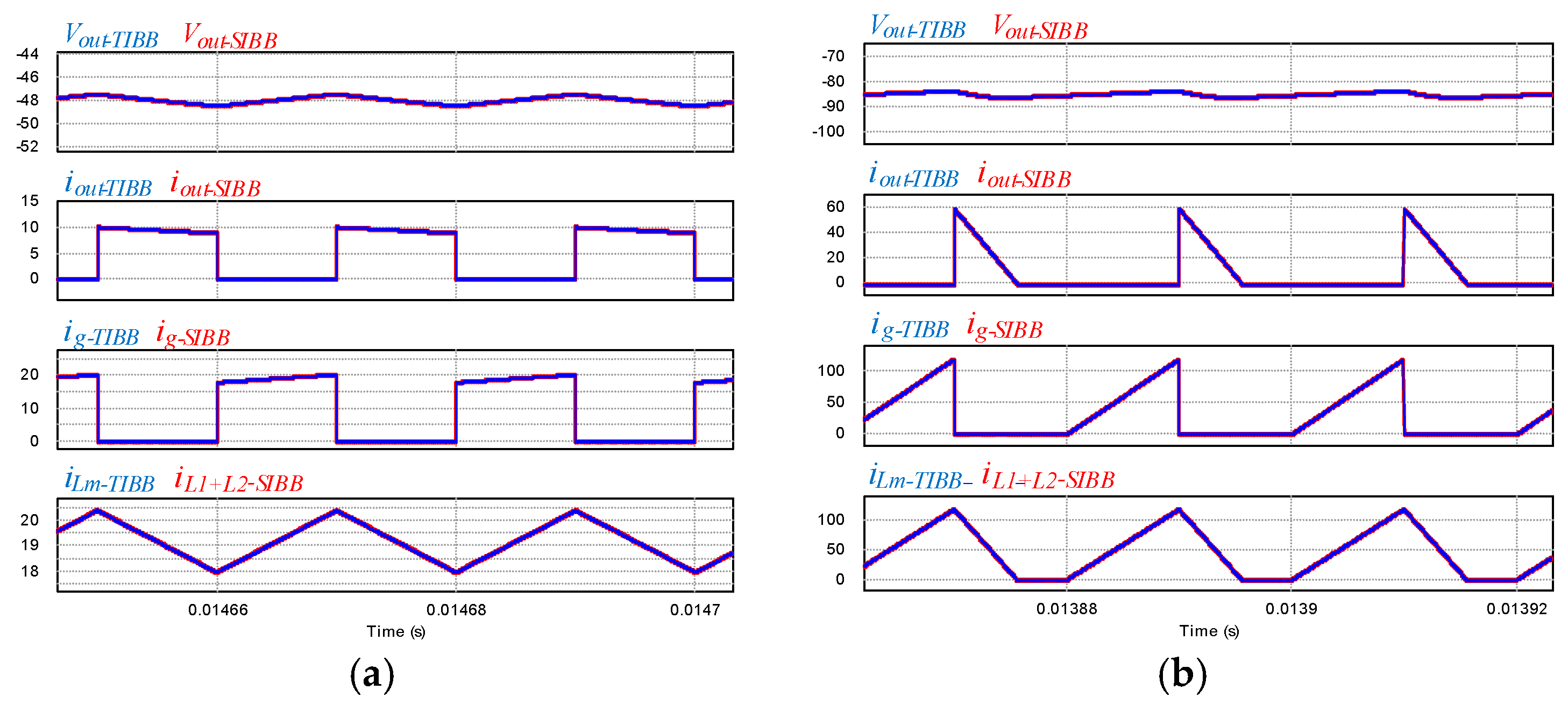
A benchmark SIBB and its equivalent TIBB were simulated in time domain. Both converters were operated with identical duty cycle, D, and had identical filter capacitor Co; identical load R; as well as identical input voltage, Vg.
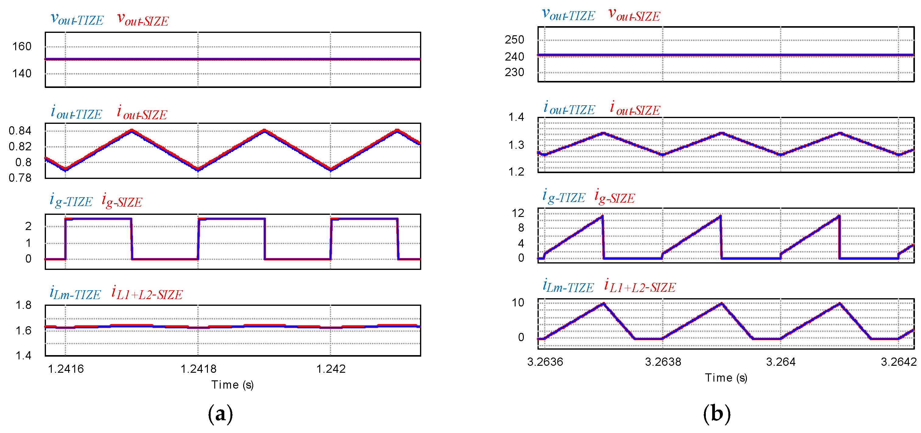
The parameters of the benchmark SIBB converter were at CCM and at DCM,, D = 0.5, R = 10 Ohm, Co = 47 μF, fS = 50 kHz. The equivalent TIBB converter parameters calculated by Equations (14) and (15) were and at CCM and at DCM. Zero leakage inductance was assumed.
Comparison of key simulated time domain waveforms of both converters in the CCM mode is shown in
Figure 9a, whereas the discontinuous conduction mode (DCM) waveforms comparison is presented in
Figure 9b. In both cases the simulated responses of both SIBB and its equivalent TIBB converters were found to be precisely identical.
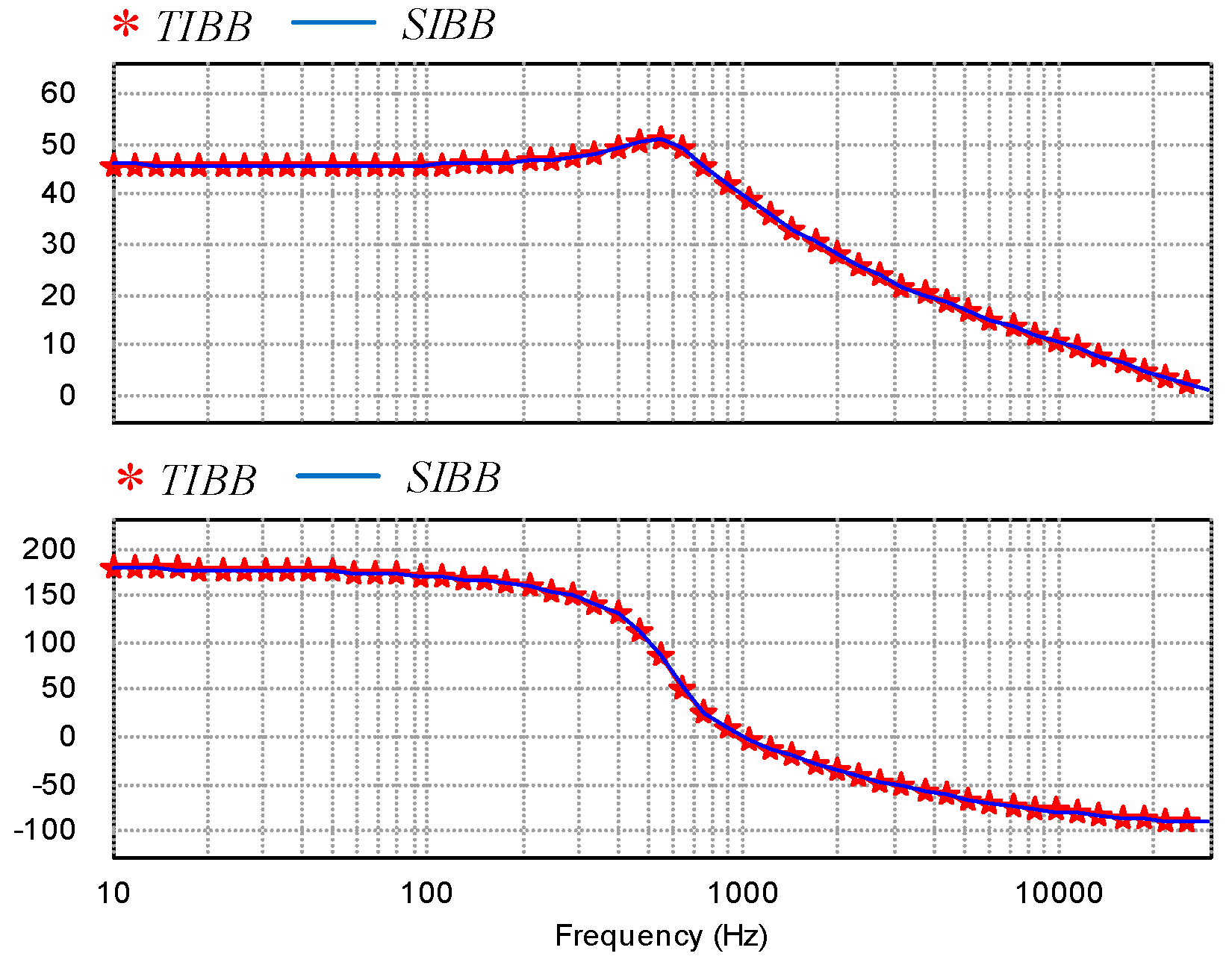
The small signal duty-cycle to output frequency response of the ideal SIBB and that of its equivalent ideal TI Buck-Boost converters was also compared and is plotted in
Figure 10. The results are precisely matched. Thus, the simulation results further support the notion of the equivalence of SIBB and TIBB converters.
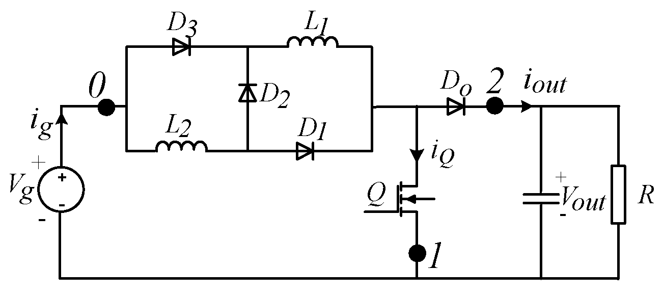
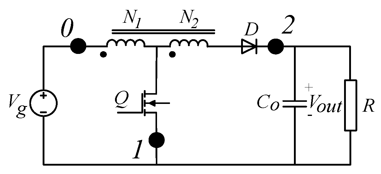
5. Equivalence of the SI Boost and TI Boost Converters
The SI Boost (SIB) converter shown in
Figure 11 and its equivalent TI Boost (TIB) converter in
Figure 12 were analyzed earlier [
21]. Here, for completeness of this text, only the equivalence conditions between SIB and TIB are briefly mentioned.
The SIB in
Figure 11 applies the step-up SI cell, the same as SIBB in
Figure 7. Hence, applying the same considerations as described in the previous section, the equivalence conditions of the SIB and TIB are found identical to Equations (14) and (15), where the magnetizing inductance
Lm is referred to the
N1 winding of TI in
Figure 12. The basic hybrid converters with switched-inductor cells and their equivalent tapped-inductor counterparts were presented in
Table 1.
6. High Order SI Converters and Their Equivalent TI Counterparts
The SI step-up and SI step-down cells in
Figure 1 can be applied to modify many other converters as well [
23,
24,
25]. The SI variants of Cuk, Sepic, and Zeta topologies were also derived in [
26]. Yet, constructing the TI equivalent counterparts of these topologies requires deeper consideration.
Firstly, consider the step-down converters. According to [
6], the SI Cuk in
Table 2 (a) applies the SI cell in
Figure 1a, whereas the SI SEPIC in
Table 2 (b) makes use of SI cell in
Figure 1b. However, as mentioned, both cells are identical (except for the polarity of the output voltage) therefore, both circuits in
Table 2 (a) and (b) can be considered identical. For this reason, both converters have the same TI equivalent counterpart as illustrated in
Table 2 (d) and (e). The step-down SI Cuk and its TI counterpart are shown in
Table 2 (e) and (f).
Next, refer to the step-up SI Cuk, Sepic, and Zeta converters in
Table 2. These topologies comprise of a series capacitor in between the active switch and the output diode (the passive switch). Thus, in these cases, the simple tap-to-switch TI arrangement used to construct the equivalent TI Cuk and the equivalent TI Sepic converters (see
Table 2 (d) and (e)) cannot be applied. Using two active switches makes it possible but such a scheme undermines the idea of equivalence. Therefore, in order for the equivalent TI converter to retain the single switch feature, a special “two-terminal” tapped inductor configuration can be applied to substitute the step-up SI cell, as shown in
Table 2 (j), (k), and (l).
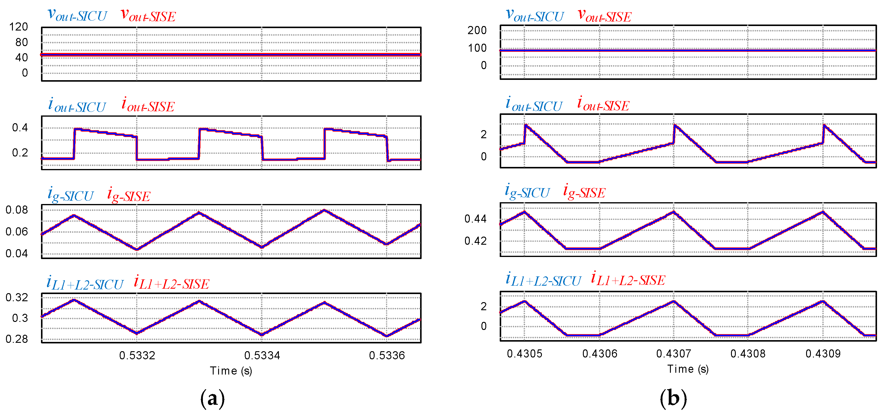
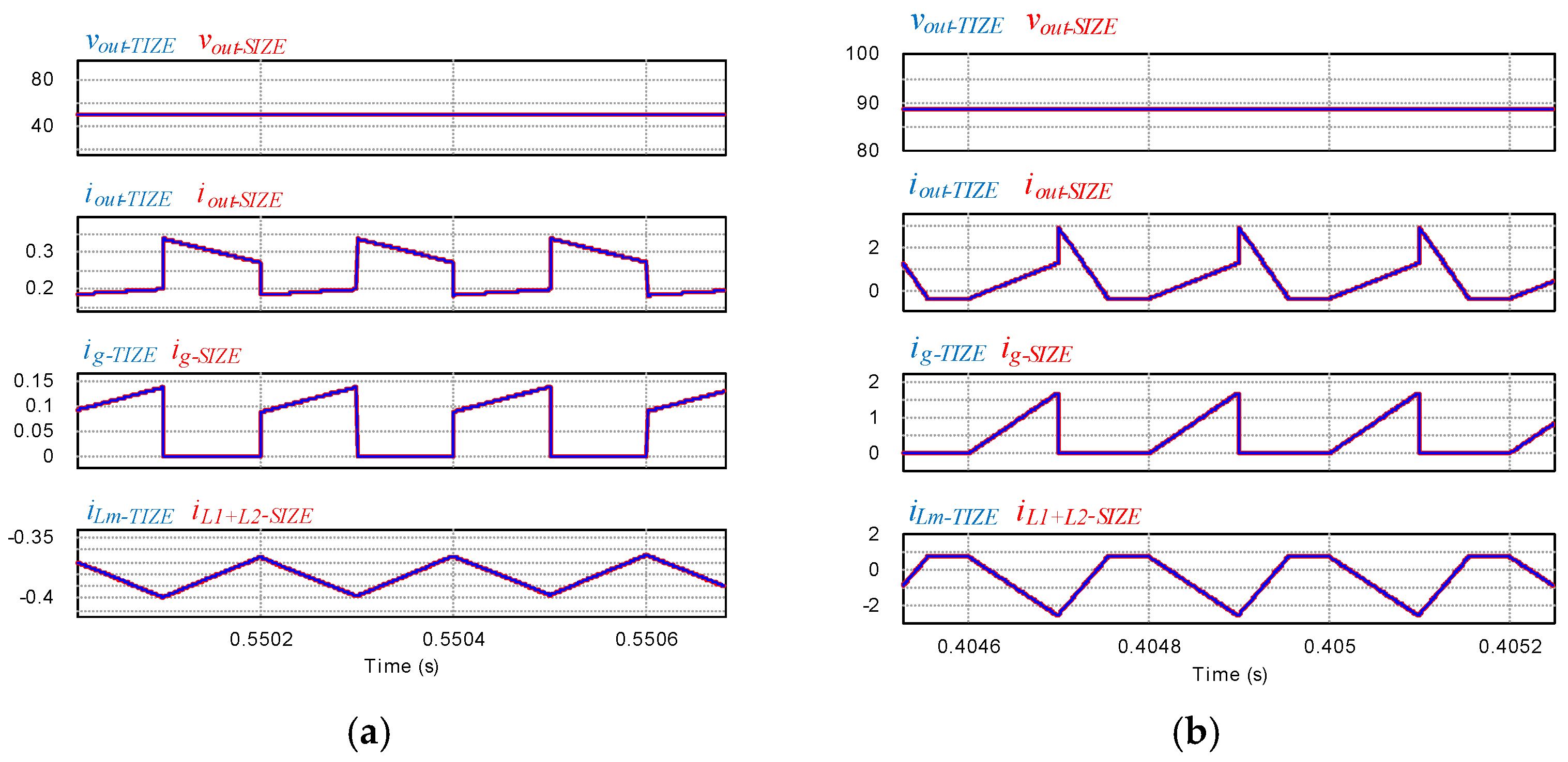
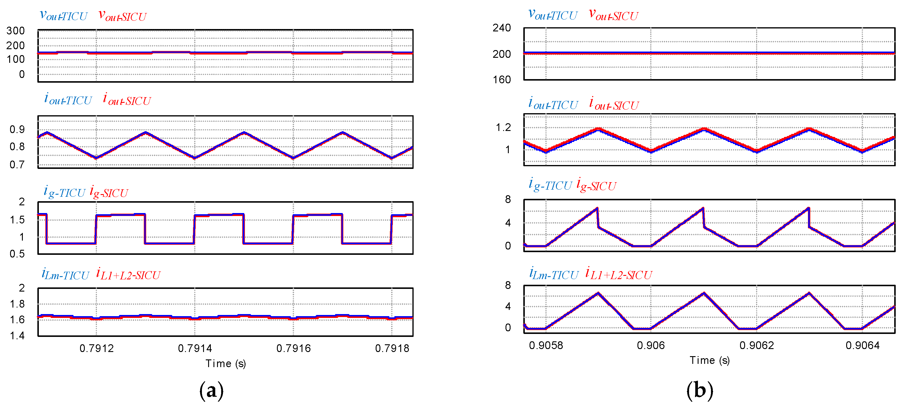
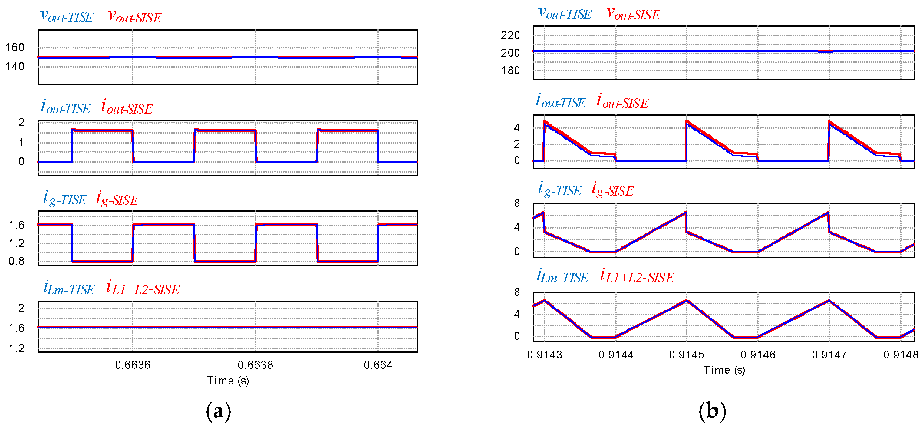
The derived above rules of equivalence Equations (5)–(7), (14) and (15)) also apply to the high order step-up and step-down converters. A simulation study was launched to compare the SI topologies to their proposed TI equivalent counterparts in
Table 2. The simulated waveforms are presented in
Appendix A which confirm the theoretical predictions.
7. Application to Small Signal Modelling of Switch Inductor Converters
Switched inductor cells consist of two inductors and multiple diodes. The switching action brings complications to modeling. Due to the equivalence of switched inductor and tapped inductor converters, the dynamic and steady state model of the SI converters can be obtained by borrowing and adapting the models of the equivalent TI counterpart. Earlier, an approach to modelling of tapped inductor converters was suggested in [
22]. The proposed Tapped Inductor Switcher with Switched Flow Graph (TIS-SFG) method relies on substituting the switching part of the converter by a prefabricated equivalent subgraph. Such modeling approach proved expeditious and well-suited to tapped inductor converters. For these reasons TIS-SFG is also a viable candidate to modeling of SI converters.
While in [
21] a step-up SI cell was examined and modeled by the proposed method, here, with the aim to extend the method further, the step-down SI cell is studied in detail. As an application example, in the following, small-signal model of the SI Buck is derived and verified by simulation and experiment.
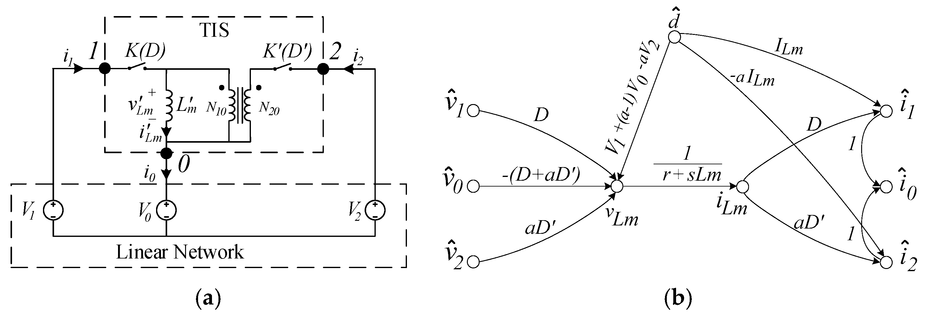
7.1. Brief Review of TIS-SFG Modeling Approach
The TIS-SFG method relies on point-by-point substitution of the tapped inductor switching block of the converter (see
Figure 13a) by its equivalent sub-graph shown in
Figure 13b. Here,
K(D) represents the active switch function and placed at terminal 1, while
K’(D’) stands for the passive (or complementary) switch at terminal 2. The common terminal is designated 0. Once the switcher, which is the problematic part of the converter, is modeled, the rest of the converter circuit is just a linear circuit and easily lends itself to modelling. To clarify the modeling procedure, an example of switched inductor Buck converter is presented as below.
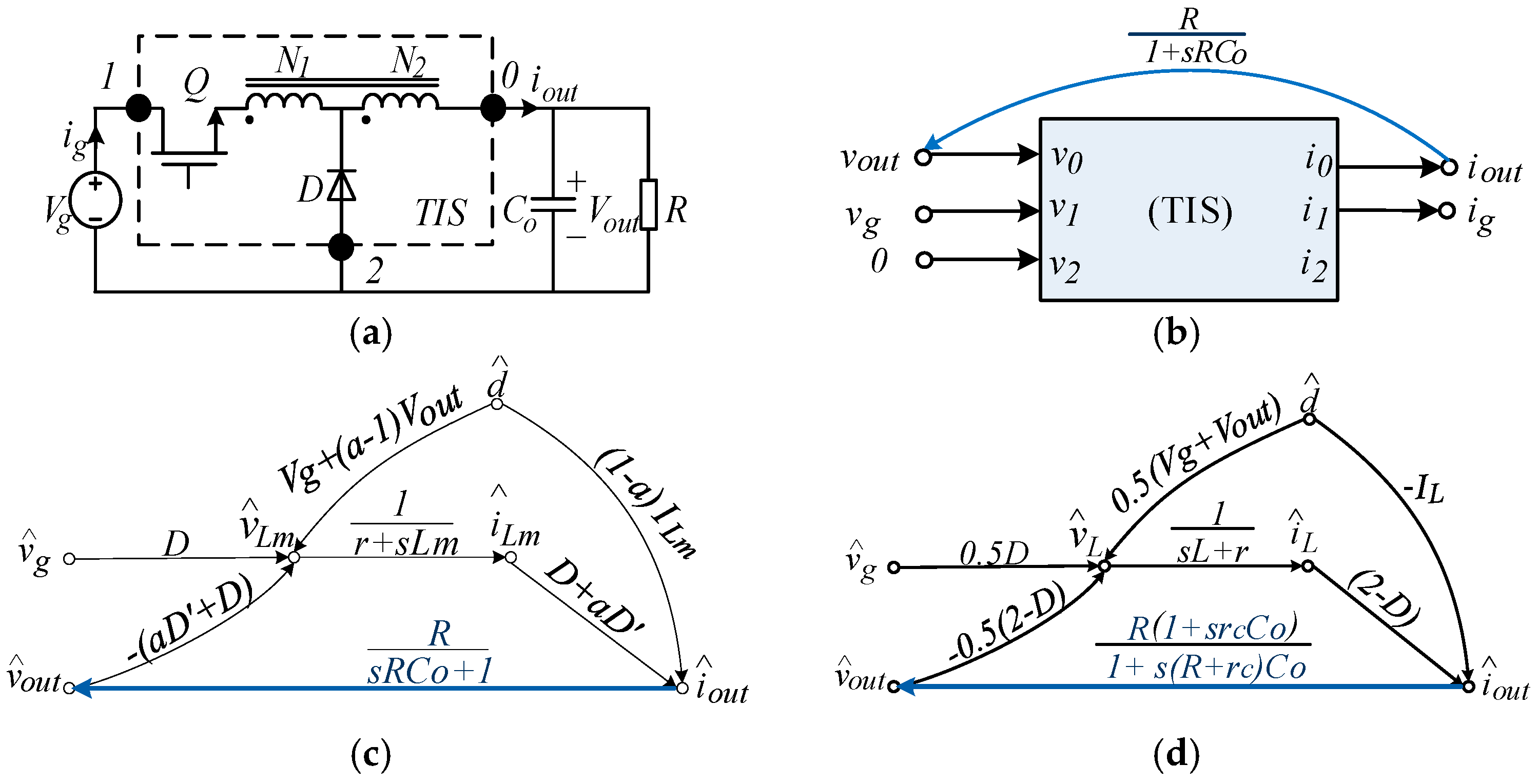
7.2. Example: TIS SFG Dynamic Models of TIBk and SIBk
As mentioned above, the SIBk converter in
Figure 3 is equivalent to the TIBk converter in
Figure 4 which has same frequency response and steady state performance, thus, the SIBk model is identical to the model of an ideal TIBk. The latter can be derived by the TIS-SFG method [
22]. First, the switching part of the converter is symbolically substituted by the TIS block, complemented by the flow graph of the linear part of the converter as shown in
Figure 14b. Here the output filter and load are modeled by a single equivalent branch (shown in blue). Then the TIS-SFG small signal model in
Figure 13b is point-to-point substituted into
Figure 14b. simplification of the graph yields the averaged small signal model of the TIBk converter as illustrated in
Figure 14c. The ideal model in
Figure 14c does not account for the capacitor’s equivalent series resistance (ESR) as well as for parasitic resistances of the inductor and the switches.
Note that the capital letters in
Figure 14c designate the steady-state values, whereas the hatted variables designate the small-signal variations of the respected quantities. For instance, the steady state duty cycle is labeled
D and its small-signal variation by
. As usual
D’ = 1 −
D.
As shown above, with the parameters properly adjusted, the dynamic model of SIBk converter is identical to that of the TIBk converter. Hence, the small-signal averaged model of the SIBk converter can be derived by applying the equivalence conditions of Equations (5), (8), and (9) to
Figure 14c to properly modify the equivalent inductance and the winding ratio. Note that the winding ratio,
a in
Figure 14 is defined as [
22]:
and
is the turn ratio. Substitution of Equation (6) into Equation (16), results in
a = 2. Substitution of Equations (8) and (9) into
Figure 14c, this leads to the model in
Figure 14d. Note that here, the effect of the capacitor’s equivalent series resistance (ESR),
rC, is incorporated simply by modifying the transfer function of the filter and load branch, whereas the combined effect of parasitic resistances of the switch,
rF, the diodes,
ron, and inductors,
rL, is modelled by a single inductor’s equivalent series resistor,
r. The derivation of the generalized equivalent series parasitic resistor,
r, was presented in [
22]. Here,
r can be estimated as
8. Experimental Verification
To experimentally verify the analysis above, a laboratory SIBk converter and its equivalent TIBk converter prototype were designed, built, and tested. The prototype of the SIBk converter had the following parameters: the inductors, L1 = 213.2 μH, L2 = 213.2 μH; switching frequency: fs = 46.92 Khz; input voltage: Vin = 24 V; Output capacitor: Co = 47 μF; load resistor: R = 10 Ohm. At the duty cycle of D = 0.5014 the circuit was operated in CCM. The measured output dc voltage was 7.84V and the measured efficiency was 96.01%.
The TIBk converter had the following parameters: the inductance of the primary side of the tapped inductor is LN1 = 102.89 μH, turns ratio of the tapped inductor: n = 1, the magnetizing inductance of the tapped inductor can be calculated as, Lm = = 411.56 μH; switching frequency is fs = 46.5 Khz; input voltage: Vin = 24 V, output capacitor: Co = 47 μF; load resistor: R = 10 Ohm. At the duty cycle of D = 0.5035 the circuit was operated in CCM. The measured output dc voltage was 7.68 V and the measured efficiency was 93.72%.
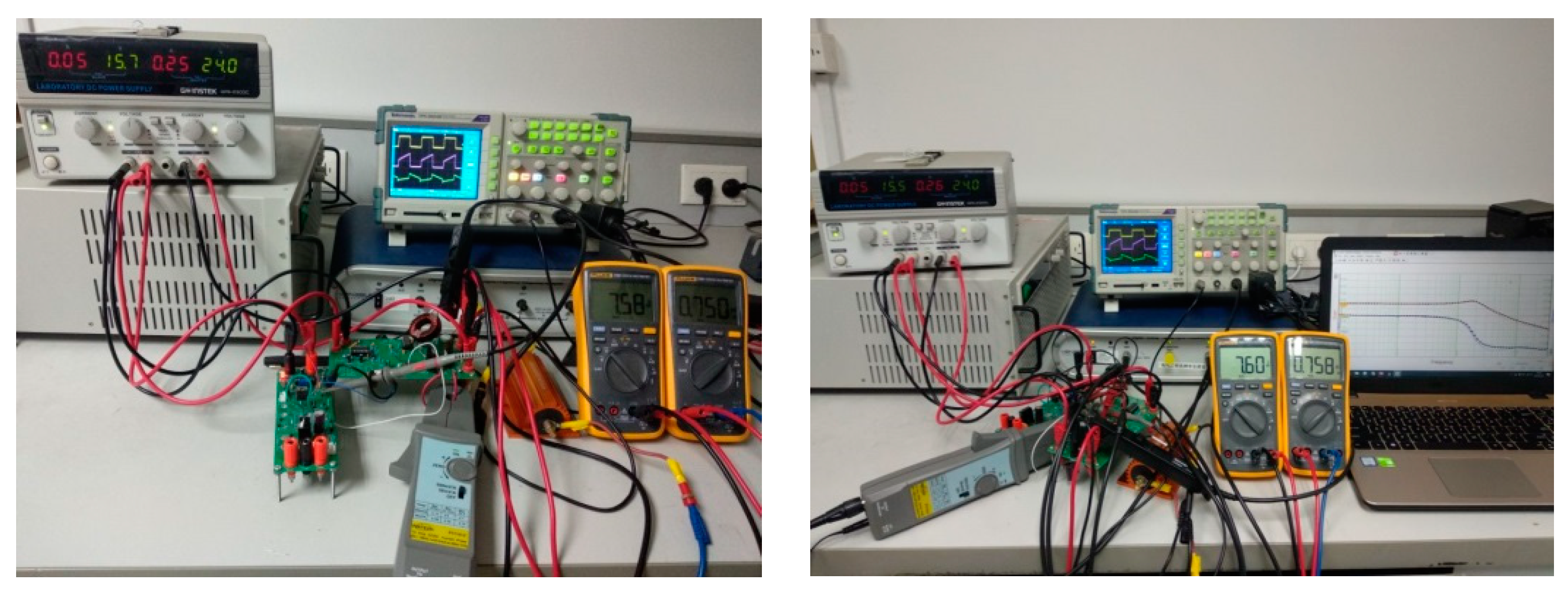
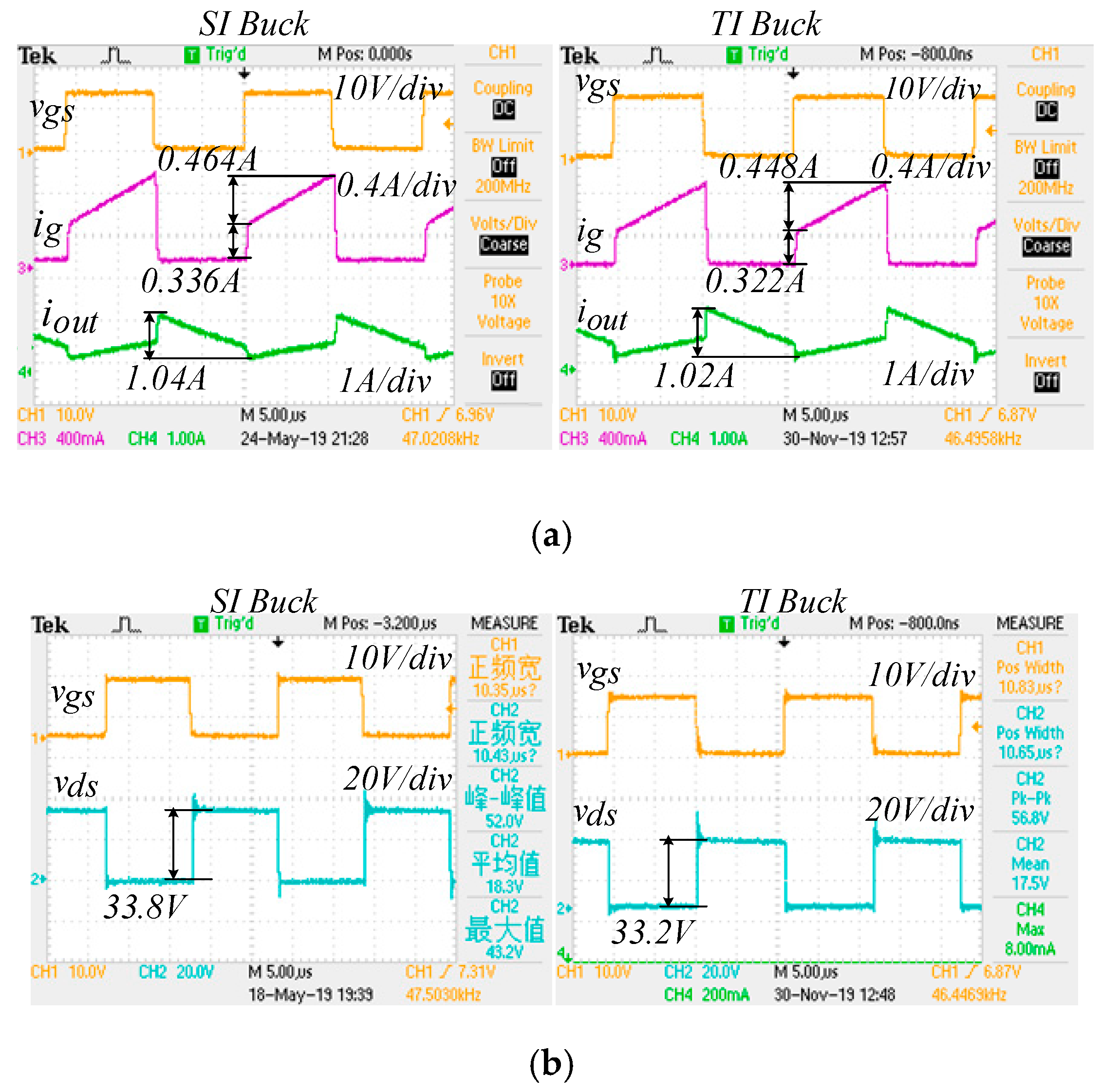
The test bench of the prototype circuit is shown in
Figure 15, while the experimental waveforms of SIBk and TIBk are shown in
Figure 16 and
Figure 17. The input current, output current of the two circuits are compared in
Figure 16a, while the voltage over MOSFET,
vds, are shown in
Figure 16b. The waveforms of the two converters are almost identical. Only a small difference is observed, except the higher voltage spike,
vds, in the TIBk circuit.
The dynamic response of the SIBk circuit was also calculated and tested. The dynamic model of SIBk in
Figure 14d requires the steady state solution data in order to calculate the gain of various branches of the model, which was derived the same as [
6]
The non-ideal small signal duty-cycle to output voltage transfer function was obtained from
Figure 14d as
where,
, , , , and .
The inductors’ resistance was measured as rL = 0.08 Ohm; the switch on resistance of the MOSFET (30N06B), is ron = 0.025 Ohm; and the diodes’ (MBR40250) forward resistance is predicted by the measured switch-on voltage drop and current which is rF = 1.12 Ohm. Plugging the aforementioned parameters into Equation (17) yields r = 0.67 Ohm.
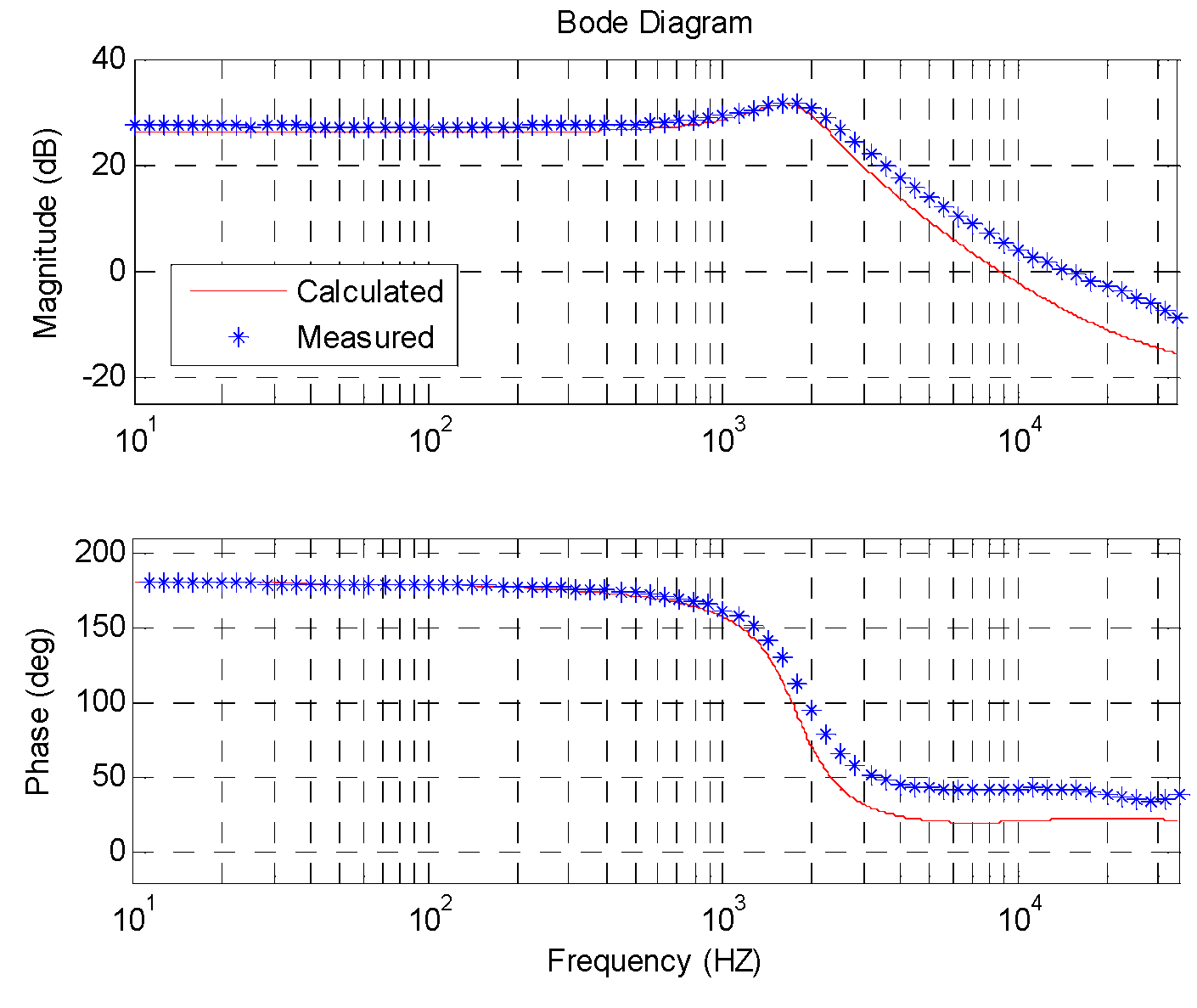
The dynamic response of the SIBk circuit was measured by Venable 8805 frequency response analyzer. The comparison of the calculated vs. experimentally measured responses is shown in
Figure 17. The predicted response is well matched to the measurements and correctly predicts the gain peaking. Yet, some deviation can be seen at high frequency range due to uncertainties in the component values and the increase in the ac resistance of the inductors at high frequency.
9. Conclusions
The paper is concerned with the analogy existing in between the switched inductor converters and the tapped inductor converters. The equivalent counterparts were proposed and examined. The rules of equivalence were derived for several study cases: Switched Inductor modified Buck, Buck-Boost, Boost converters as well as Cuk, Sepic, and Zeta derived converters.
Practical implication of the proposed equivalence hypothesis is extending the TIS-SFG modelling approach [
22], conceived for the TI converters, to include switched inductor converters as well. This paper illustrates the small signal modelling of the step-down SI cell to complete the step-up SI cell counterpart model demonstrated earlier [
21]. As an example, SI Buck converter is analyzed theoretically and confirmed vs. simulated and experimental results.
The equivalence of TI and SI converters is somewhat limited in reality since the practical TI converters are prone to the problems of the leakage inductance. This, however, presents no hindrance to the suggested methodology of small-signal modeling the SI converters. As mentioned, SI converters have no leakage and, for this reason, the small-signal model of SI converter derived from the ideal (i.e., leakage-free) TI model attains accurate results in reality. Hence, taking advantage of the equivalence feature, and using the TIS model as a tool, can facilitate the small-signal analysis of SI converters.
Theoretical expectations were confirmed by an extensive cycle-by-cycle simulation study. The time-domain waveforms of the ideal switched inductor converters were compared and perfectly matched the waveforms of their equivalent ideal tapped-inductor counterparts. The equivalence holds in both continuous and discontinuous operating modes. Moreover, the performance of the Buck, Boost, and Buck-Boost equivalent converters in the frequency domain was also examined. The duty-cycle-to-output-frequency response of the switched inductor converters was simulated and compared to the response of their tapped inductor counterparts and, as expected, was found identical. Comparison of the experimental results for SIBk and TIBk converters was also reported. A good match was observed.


 (a)
(a) (b)
(b) (c)
(c) (d)
(d) (e)
(e) (f)
(f) (g)
(g) (h)
(h) (i)
(i) (j)
(j) (k)
(k) (l)
(l)