A Metal Object Detection System with Multilayer Detection Coil Layouts for Electric Vehicle Wireless Charging


Abstract
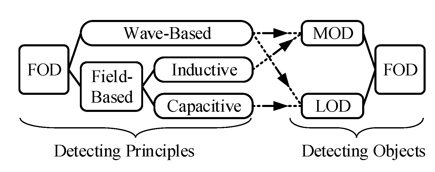
:1. Introduction
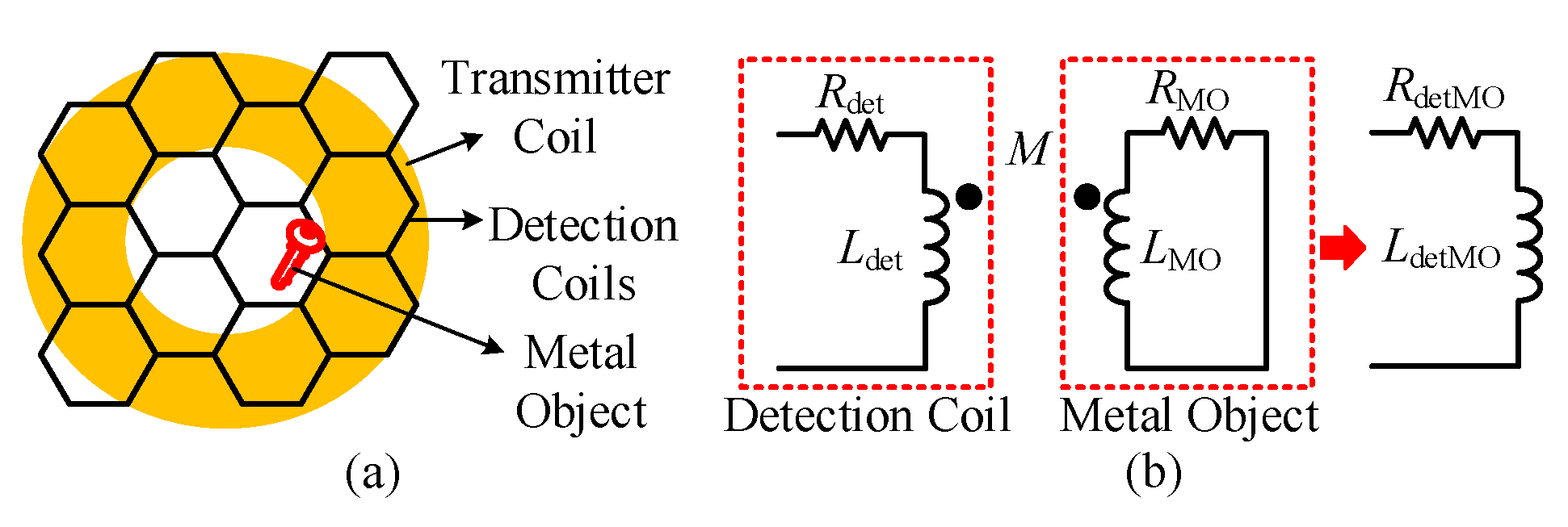
2. Detection Coil Array
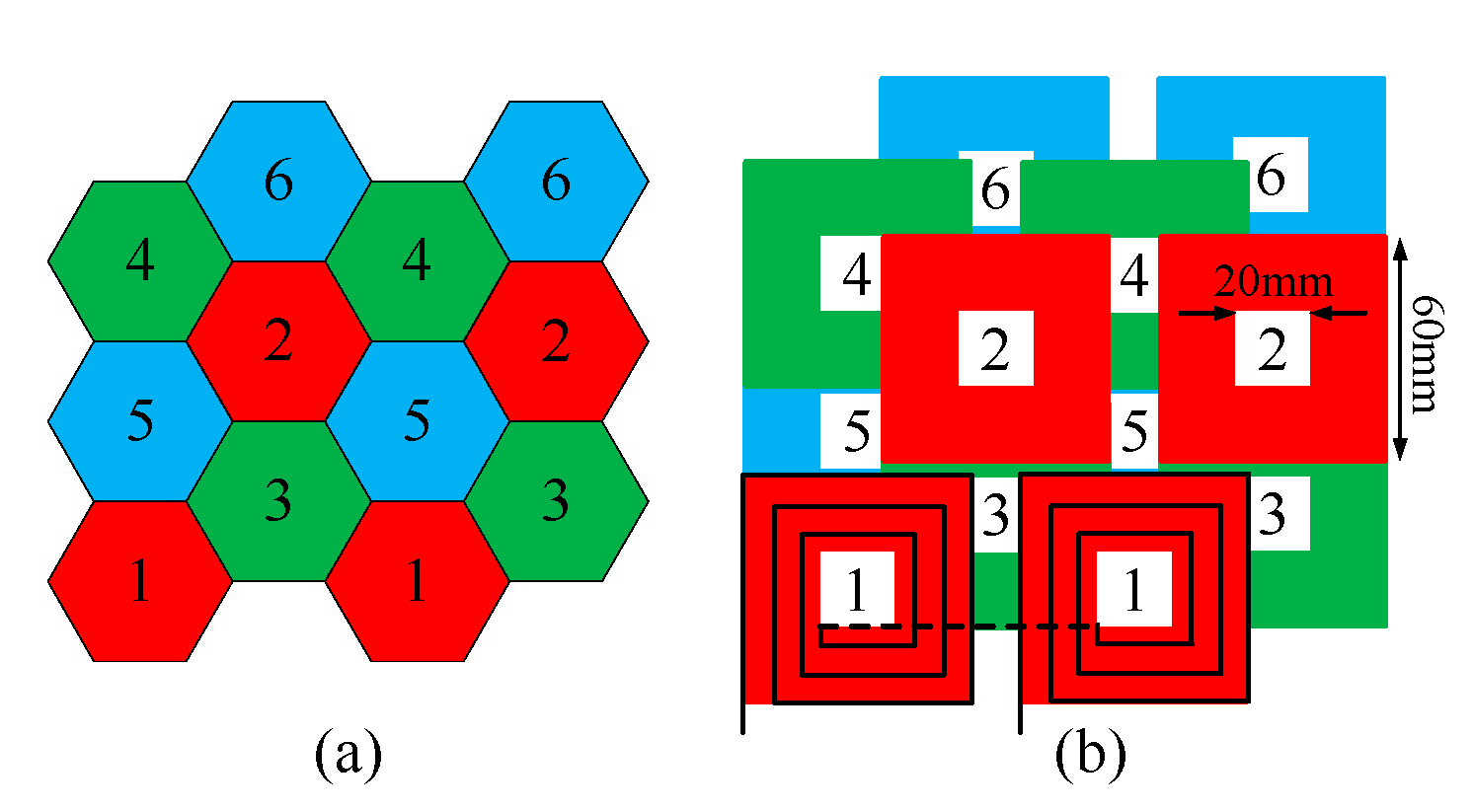
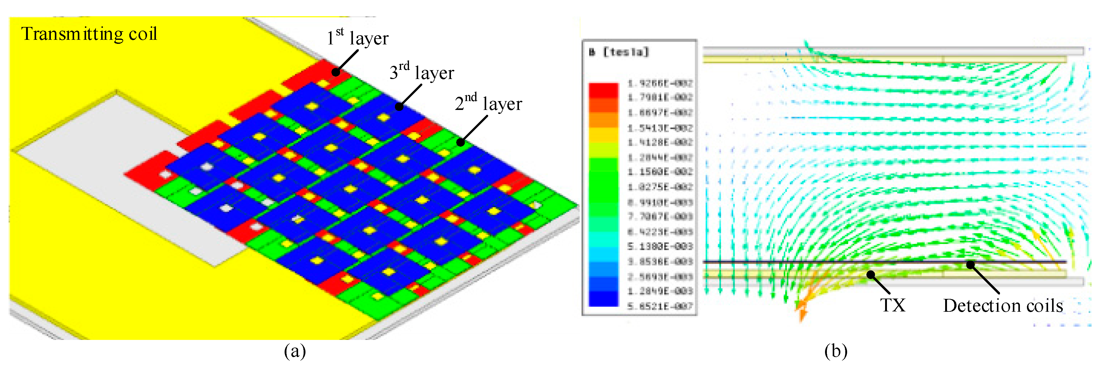
2.1. Three-Layer Hexagonal Layout Detection Coils
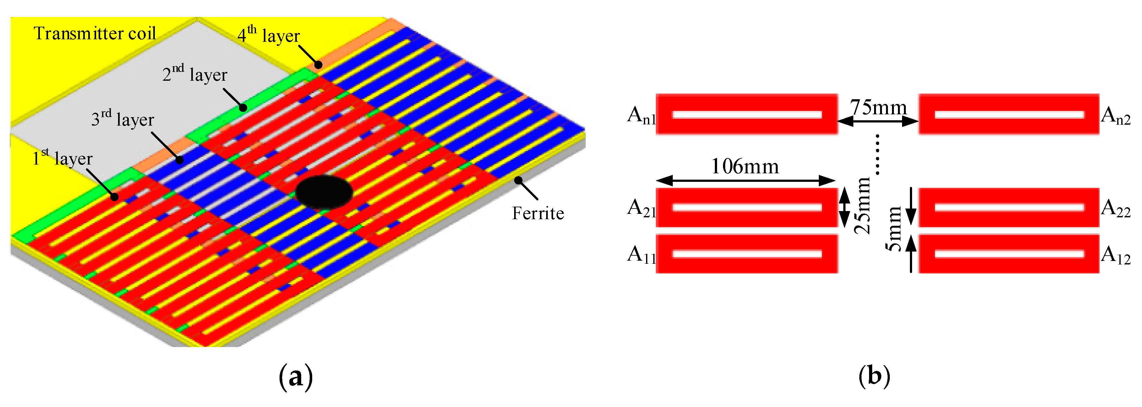
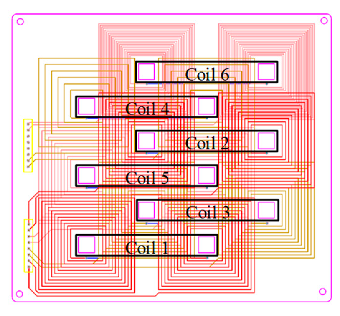
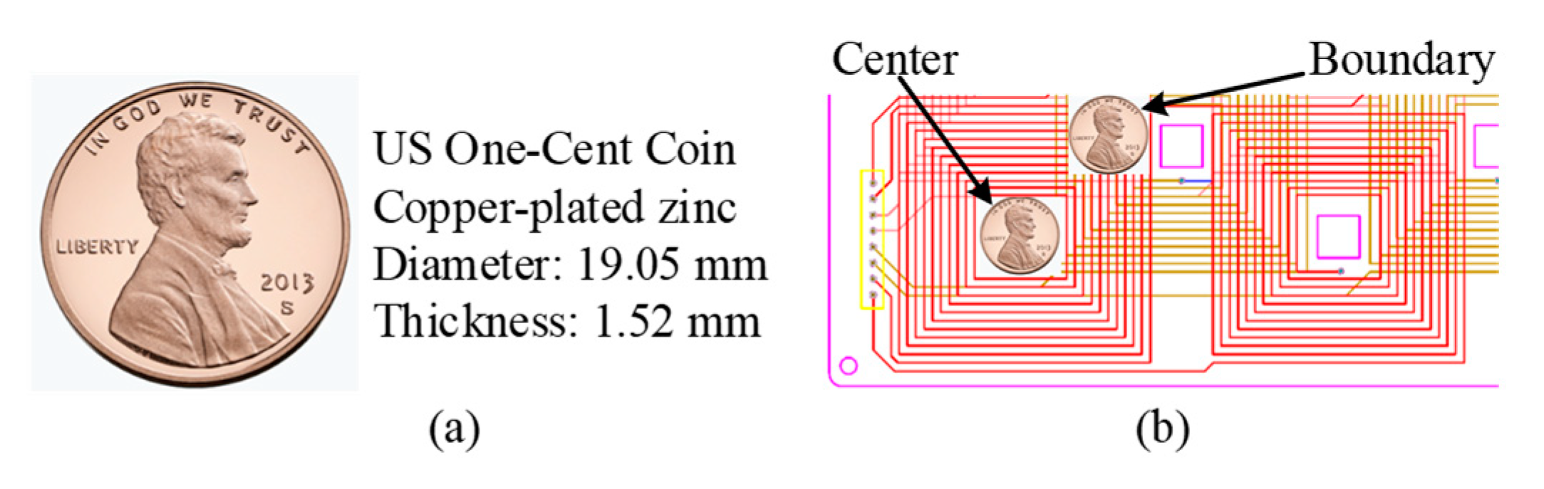
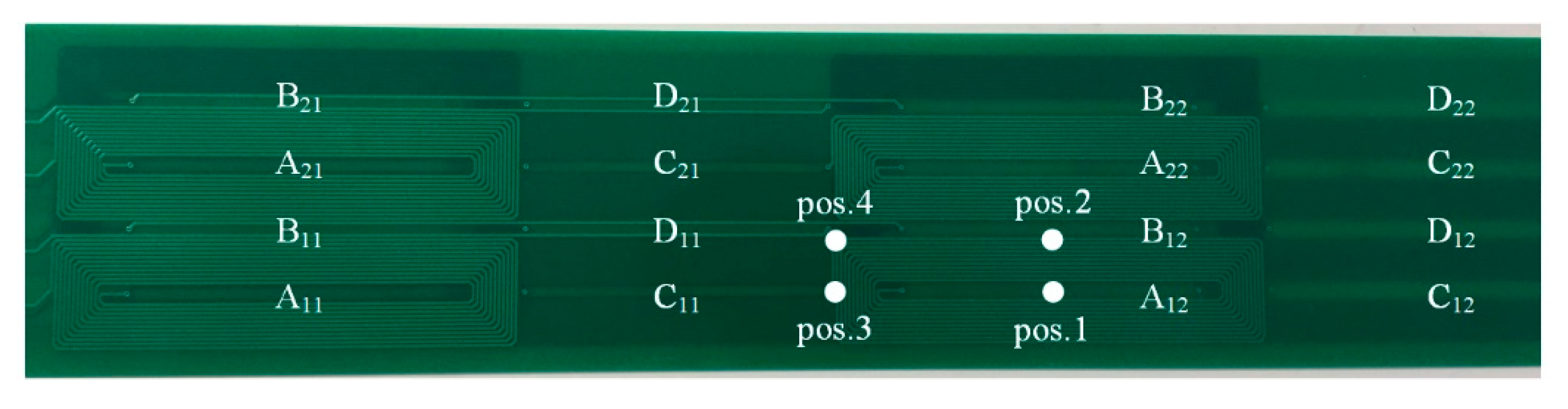
2.2. Four-Layer Rectangular Layout Detection Coils
3. Principle of Detection
3.1. Inductance Variation
3.2. Mixed Resonances
3.2.1. SP Mixed Resonances
3.2.2. PS Mixed Resonances
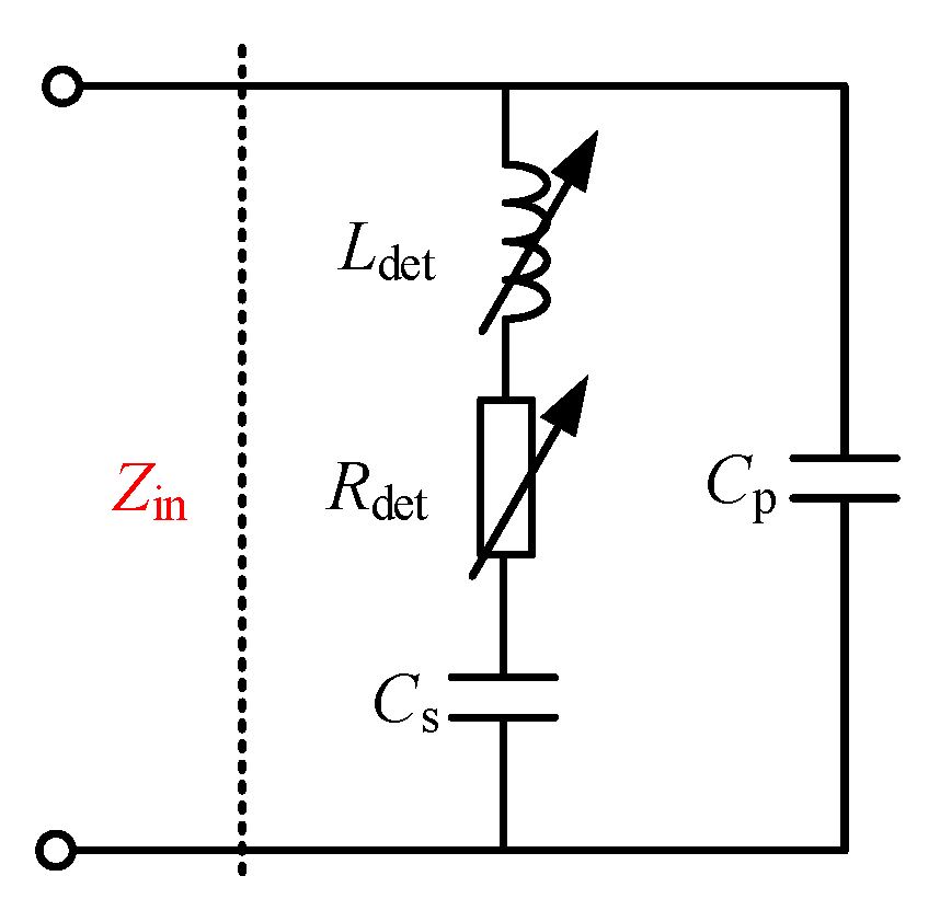
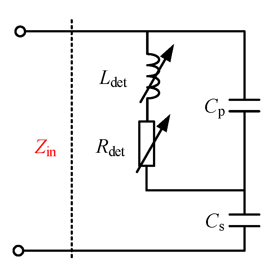
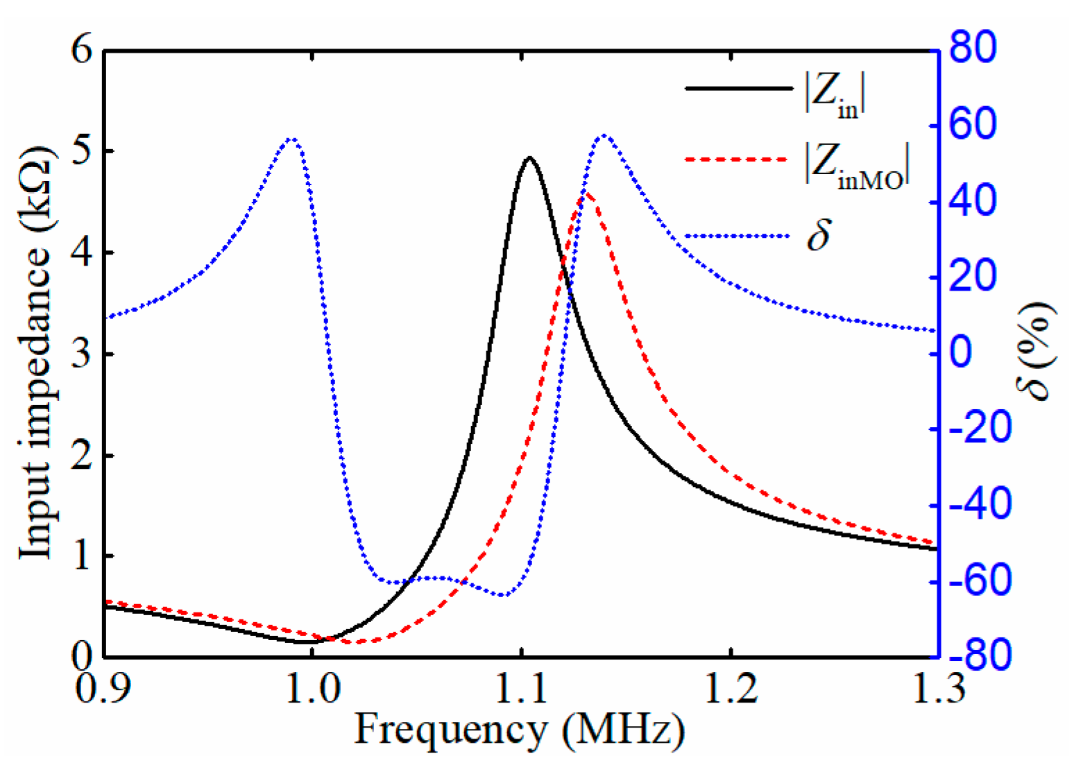
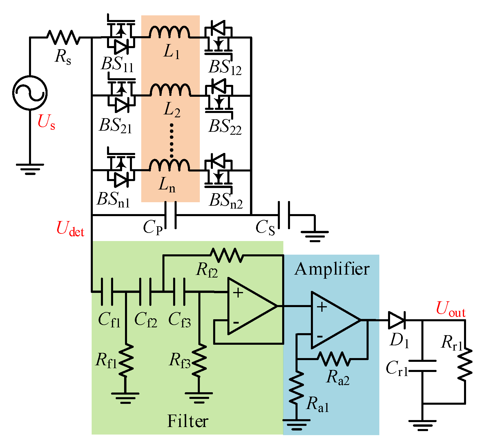
3.3. System Topology
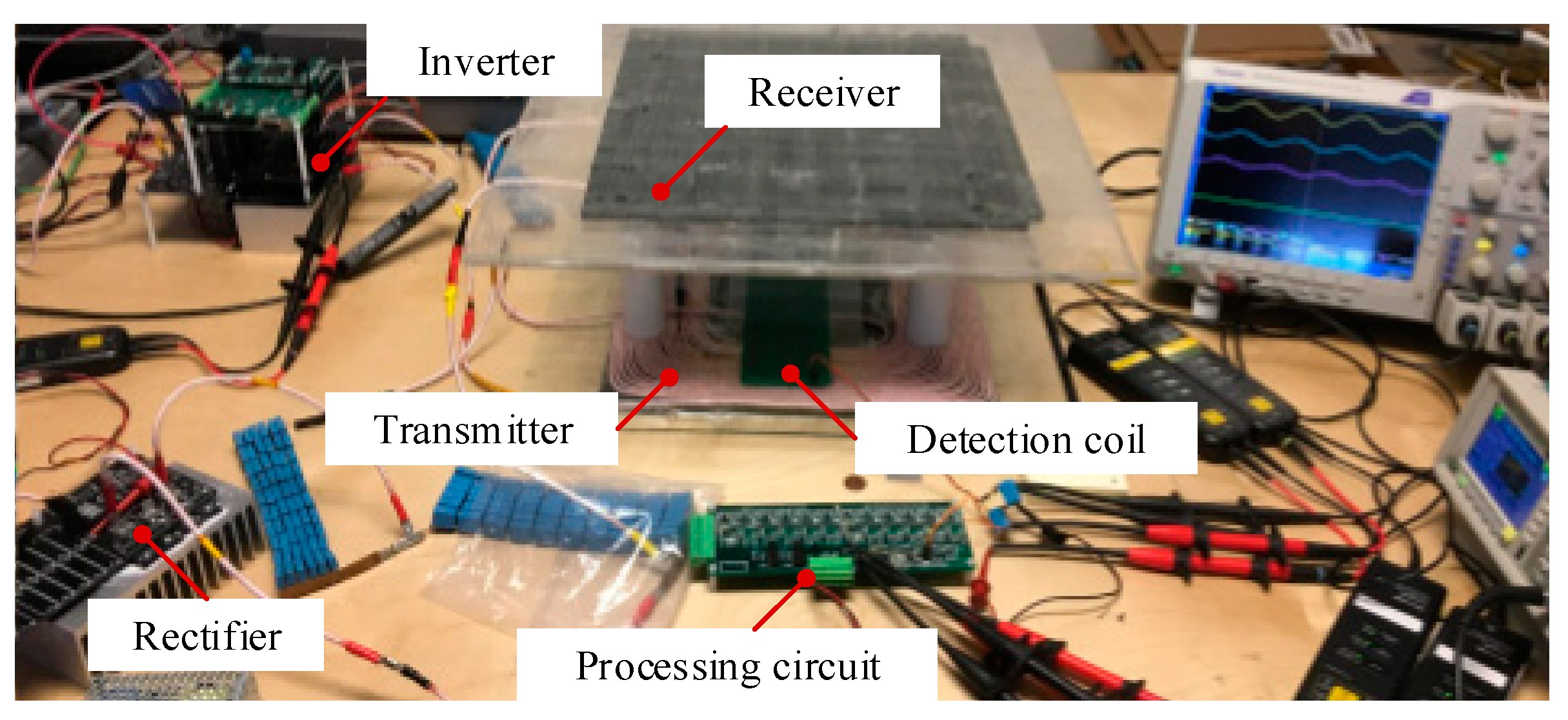
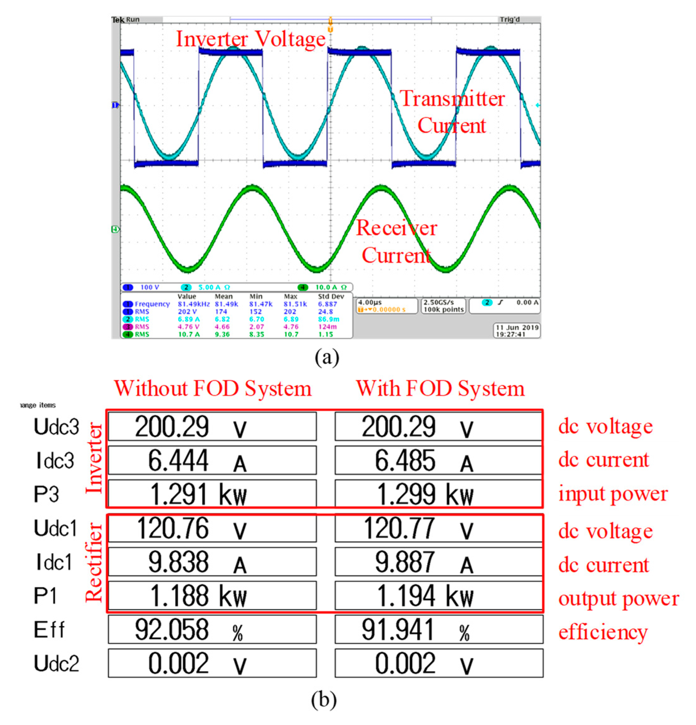
4. System Implementation and Measurement
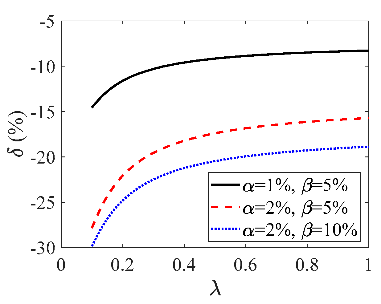
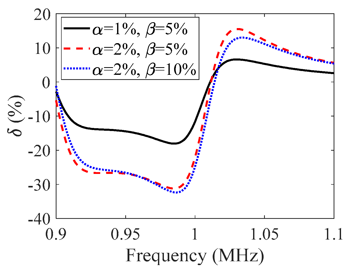
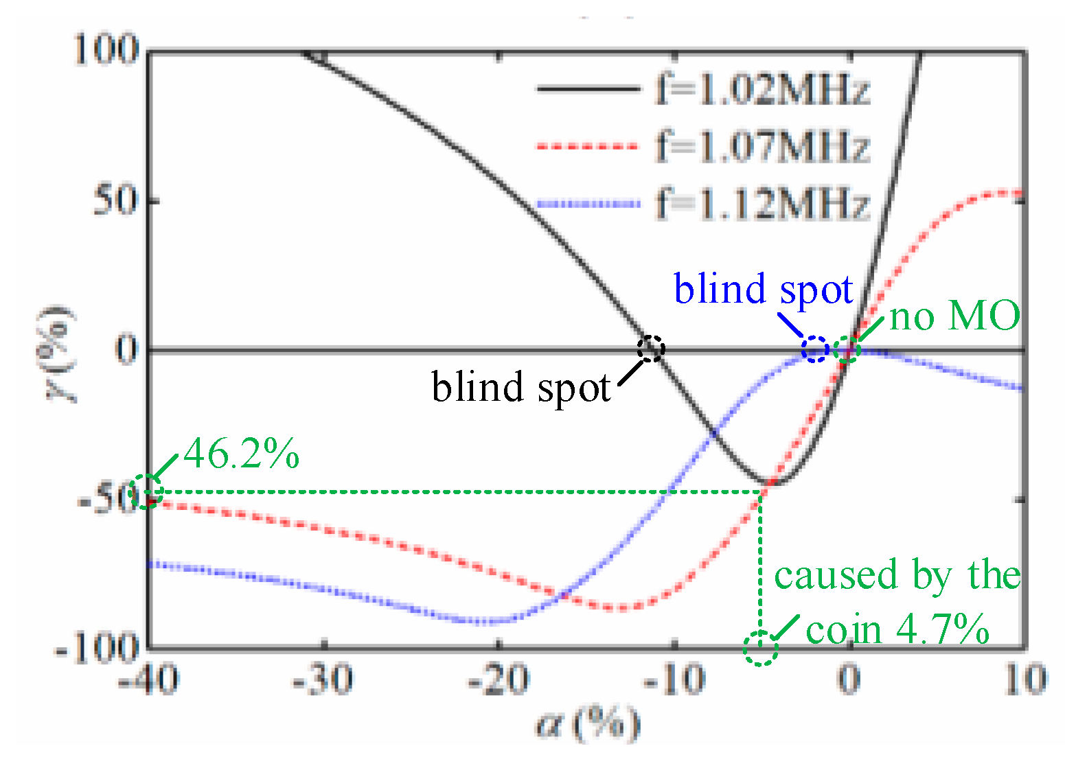
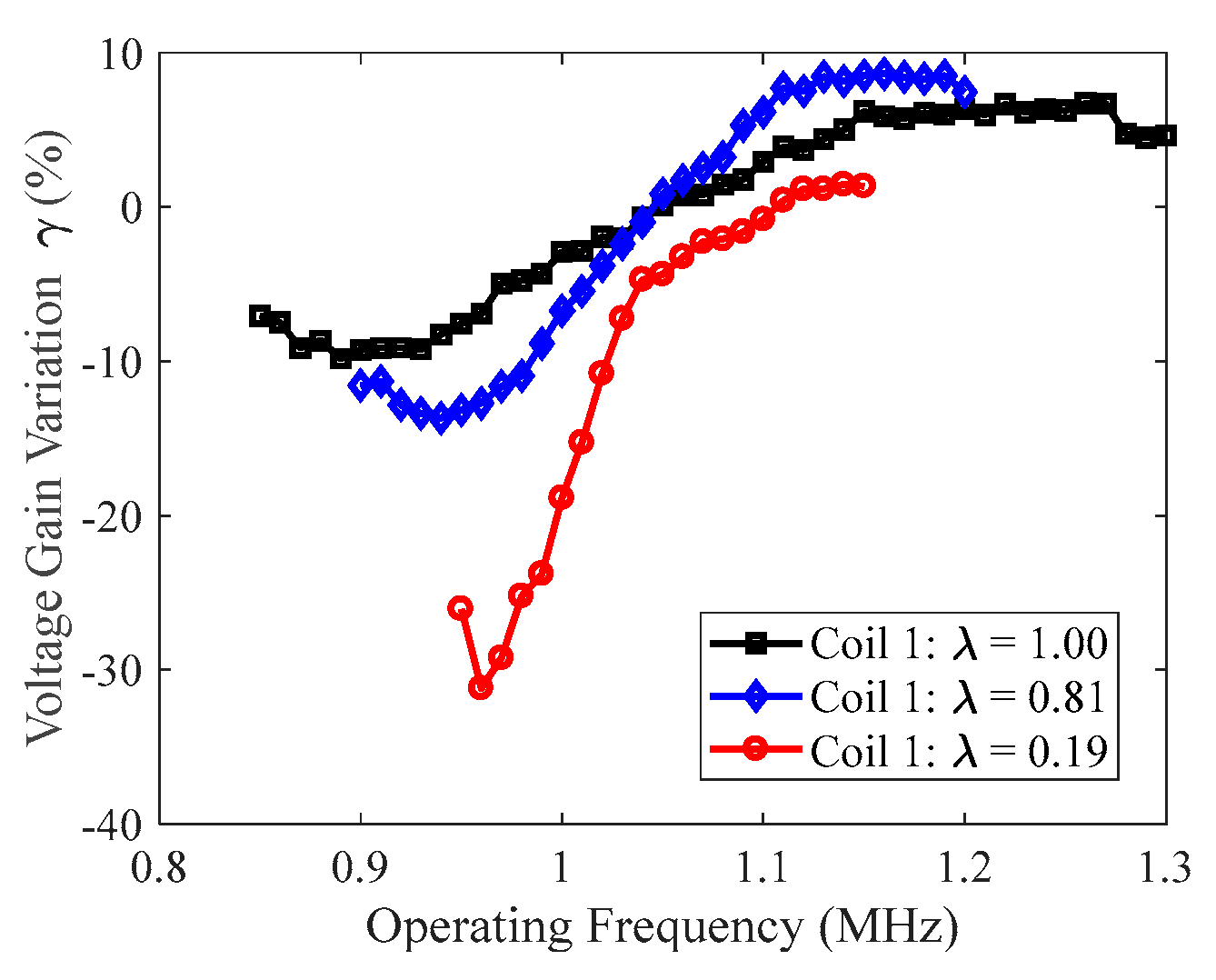
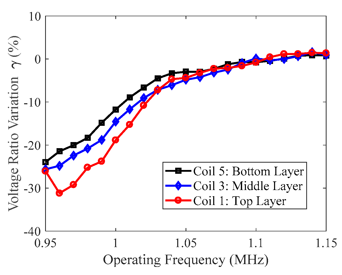
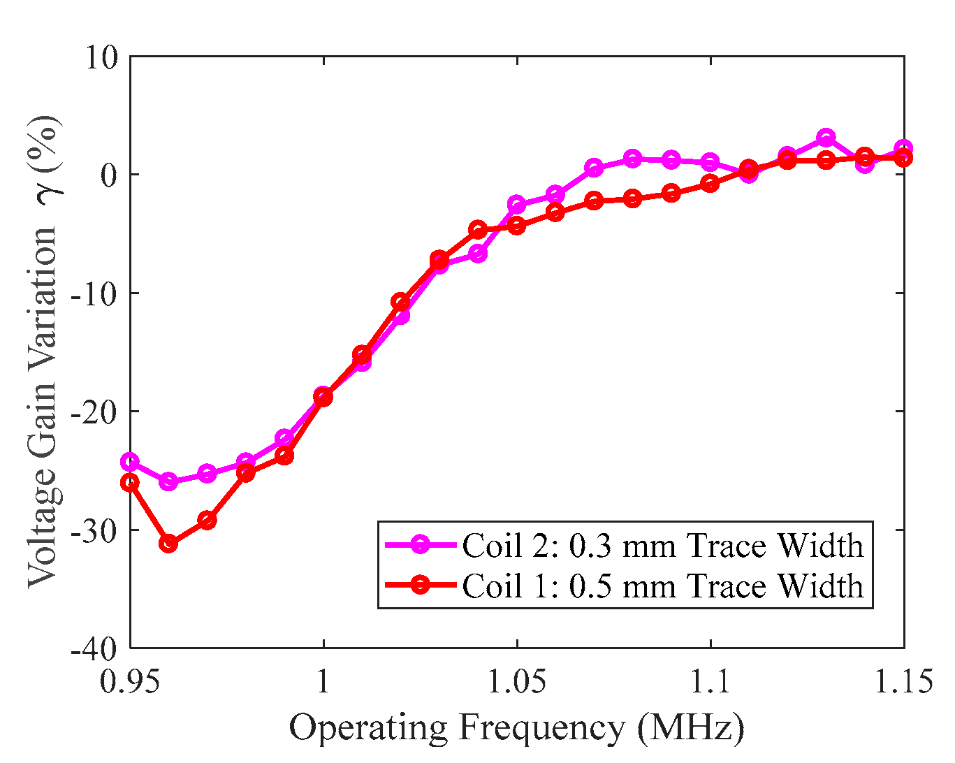
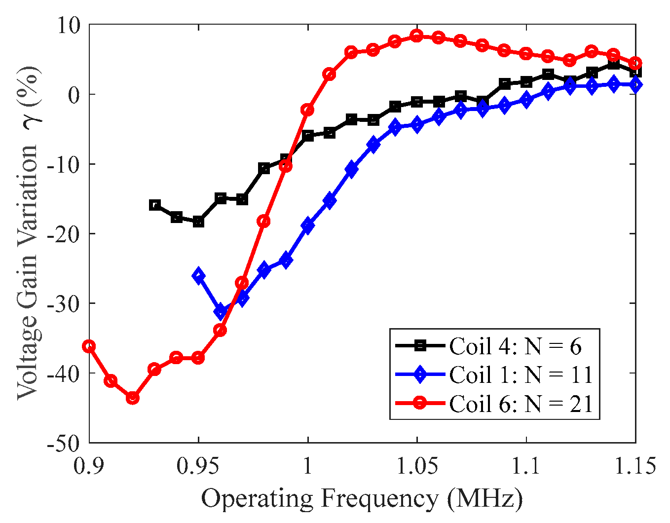
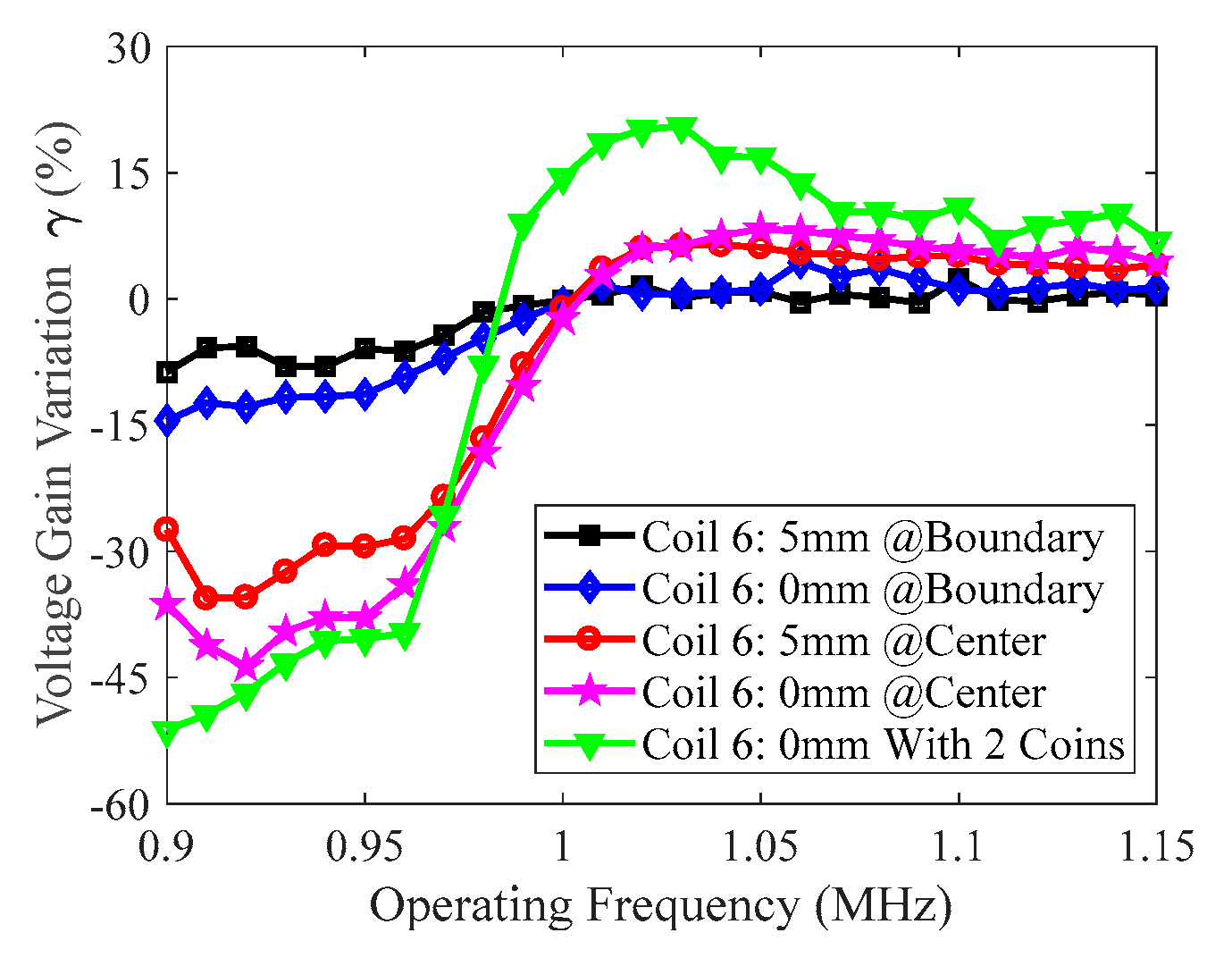
4.1. Impacts of Detection Coil Parameters
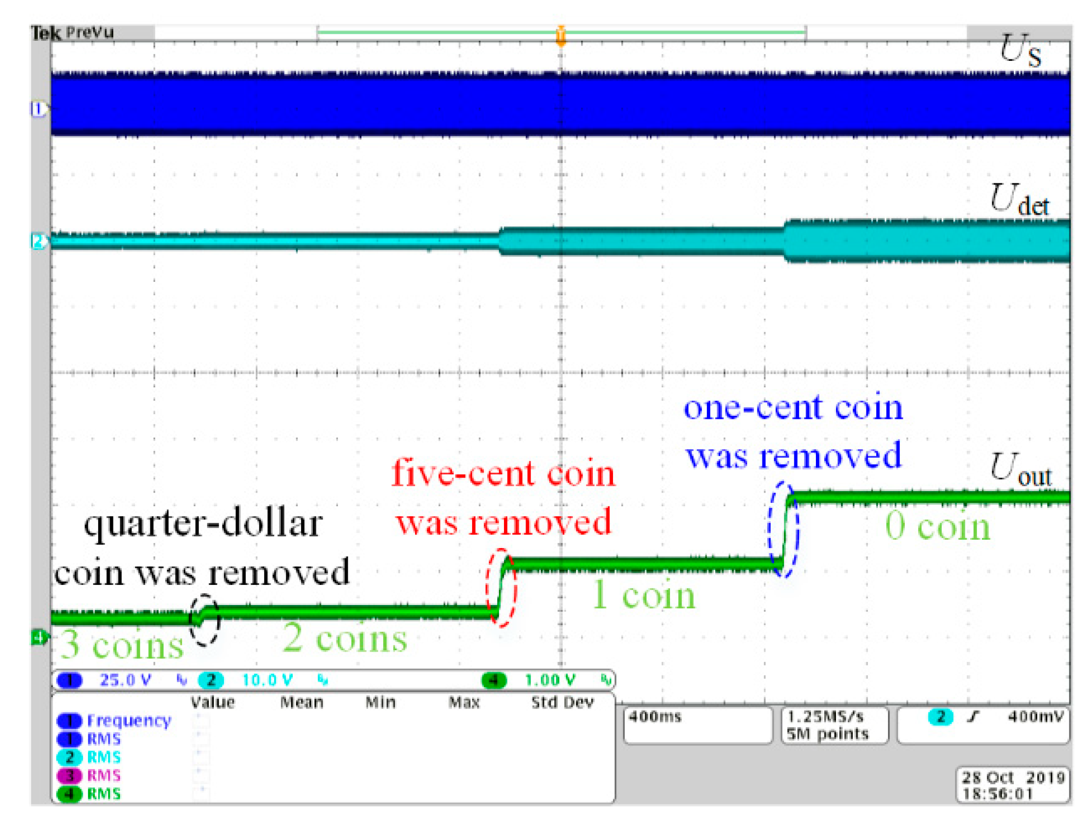
4.2. System Performance
5. Conclusions
Author Contributions
Funding
Conflicts of Interest
References
- Hui, S.R. Technical and safety challenges in emerging trends of near-field wireless power transfer industrial guidelines. IEEE Electromagn. Compat. Mag. 2018, 7, 78–86. [Google Scholar] [CrossRef]
- Bi, Z.; Kan, T.; Mi, C.C.; Zhang, Y.; Zhao, Z.; Keoleian, G.A. A review of wireless power transfer for electric vehicles: Prospects to enhance sustainable mobility. Appl. Energy 2016, 179, 413–425. [Google Scholar] [CrossRef] [Green Version]
- Covic, G.A.; Boys, J.T. Inductive Power Transfer. Proc. IEEE 2013, 101, 1276–1289. [Google Scholar] [CrossRef]
- Kan, T.; Zhang, Y.; Yan, Z.; Mercier, P.P.; Mi, C. A Rotation-Resilient Wireless Charging System for Lightweight Autonomous Underwater Vehicles. IEEE Trans. Veh. Technol. 2018, 67, 6935–6942. [Google Scholar] [CrossRef]
- Yuan, L.; Li, B.; Zhang, Y.; He, F.; Chen, K.; Zhao, Z. Maximum efficiency point tracking of the wireless power transfer system for the battery charging in electric vehicles. In Proceedings of the 2015 18th International Conference on Electrical Machines and Systems (ICEMS), Institute of Electrical and Electronics Engineers (IEEE), Pattaya, Thailand, 25–28 October 2015; pp. 1101–1107. [Google Scholar]
- Liu, C.; Jiang, C.; Song, J.; Chau, K.T. An Effective Sandwiched Wireless Power Transfer System for Charging Implantable Cardiac Pacemaker. IEEE Trans. Ind. Electron. 2018, 66, 4108–4117. [Google Scholar] [CrossRef]
- Huang, Z.; Wong, S.C.; Tse, C.K. Control Design for Optimizing Efficiency in Inductive Power Transfer Systems. IEEE Trans. Power Electron. 2018, 33, 4523–4534. [Google Scholar] [CrossRef]
- Patil, D.; McDonough, M.K.; Miller, J.M.; Fahimi, B.; Balsara, P.T. Wireless Power Transfer for Vehicular Applications: Overview and Challenges. IEEE Trans. Transp. Electr. 2018, 4, 3–37. [Google Scholar] [CrossRef]
- Onar, O.C.; Campbell, S.; Seiber, L.E.; White, C.P.; Chinthavali, M. A high-power wireless charging system development and integration for a Toyota RAV4 electric vehicle. In Proceedings of the 2016 IEEE Transportation Electrification Conference and Expo (ITEC), Institute of Electrical and Electronics Engineers (IEEE), Dearborn, MI, USA, 27–29 June 2016; pp. 1–8. [Google Scholar]
- Guo, Y.; Wang, L.; Zhang, Y.; Li, S.; Liao, C. Rectifier Load Analysis for Electric Vehicle Wireless Charging System. IEEE Trans. Ind. Electron. 2018, 65, 6970–6982. [Google Scholar] [CrossRef]
- Widmer, H.; Sieber, L.; Daetwyler, A.; Bittner, M. Systems, Methods, and Apparatus for Radar-Based Detection of Objects in a Predetermined Space. U.S. Patent 9,772,401 B2, 26 September 2017. [Google Scholar]
- Sieber, L.; Chopra, S. Systems, Methods, and Apparatus for Living Object Protection in Wireless Power Transfer Applications. U.S. Patent 2016/0109564 A1, 21 April 2016. [Google Scholar]
- Poguntke, T.; Schumann, P.; Ochs, K. Radar-based living object protection for inductive charging of electric vehicles using two-dimensional signal processing. Wirel. Power Transf. 2017, 4, 88–97. [Google Scholar] [CrossRef] [Green Version]
- Bell, D.; Leabman, M.A. Systems and Methods of Object Detection Using One or More Sensors in Wireless Power Charging Systems. U.S. Patent 10,483,768, 16 January 2018. [Google Scholar]
- Hoffman, P.F.; Boyer, R.J.; Henderson, R.A. Foreign Object Detection System and Method Suitable for Source Resonator of Wireless Energy Transfer System. U.S. Patent 9,304,042 B2, 5 April 2016. [Google Scholar]
- Karanth, A.; Dorairaj, H.H.K.; Balakrishnan, R.; Kumar, R. Foreign Object Detection in Inductive Coupled Wireless Power Transfer Environment Using Thermal Sensors. U.S. Patent 2013/0163635 A1, 27 June 2013. [Google Scholar]
- Fukuda, S.; Nakano, H.; Murayama, Y.; Murakami, T.; Kozakai, O.; Fujimaki, K. A novel metal detector using the quality factor of the secondary coil for wireless power transfer systems. In Proceedings of the 2012 IEEE MTT-S International Microwave Workshop Series on Innovative Wireless Power Transmission: Technologies, Systems, and Applications, Tokyo, Japan, 10–11 May 2012; pp. 241–244. [Google Scholar] [CrossRef]
- Jeong, S.Y.; Kwak, H.G.; Jang, G.C.; Choi, S.Y.; Rim, C.T.; Kwak, H.G. Dual-Purpose Nonoverlapping Coil Sets as Metal Object and Vehicle Position Detections for Wireless Stationary EV Chargers. IEEE Trans. Power Electron. 2017, 33, 7387–7397. [Google Scholar] [CrossRef]
- Zhang, H.; Ma, D.; Lai, X.; Yang, X.; Tang, H. The Optimization of Auxiliary Detection Coil for Metal Object Detection in Wireless Power Transfer. In Proceedings of the 2018 IEEE PELS Workshop on Emerging Technologies: Wireless Power Transfer (Wow), Montréal, QC, Canada, 3–7 June 2018; pp. 1–6. [Google Scholar] [CrossRef]
- Xiang, L.; Zhu, Z.; Tian, J.; Tian, Y. Foreign Object Detection in a Wireless Power Transfer System Using Symmetrical Coil Sets. IEEE Access 2019, 7, 44622–44631. [Google Scholar] [CrossRef]
- Sieber, L.; Fischer, M.; Widmer, H. Systems, Methods, and Apparatus for Increased Foreign Object Detection Loop Array Sensitivity. U.S. Patent 9,921,045 B2, 20 March 2018. [Google Scholar]
- Jeong, S.Y.; Kwak, H.G.; Jang, G.C.; Rim, C.T. Living object detection system based on comb pattern capacitive sensor for wireless EV chargers. In Proceedings of the 2016 IEEE 2nd Annual Southern Power Electronics Conference (SPEC), Institute of Electrical and Electronics Engineers (IEEE), Auckland, New Zealand, 5–8 December 2017; pp. 1–6. [Google Scholar]
- Jeong, S.Y.; Thai, V.X.; Park, J.H.; Rim, C.T. Self-Inductance-Based Metal Object Detection With Mistuned Resonant Circuits and Nullifying Induced Voltage for Wireless EV Chargers. IEEE Trans. Power Electron. 2018, 34, 748–758. [Google Scholar] [CrossRef]
- Chopra, S. Percebon, L. Dynamic Mutual Sensing Foreign Object Detection Loops. U.S. Patent 2018/0076671 A1, 15 March 2018. [Google Scholar]
- Khan, S.R.; Pavuluri, S.K.; Desmulliez, M.P. Accurate Modeling of Coil Inductance for Near-Field Wireless Power Transfer. IEEE Trans. Microw. Theory Tech. 2018, 66, 4158–4169. [Google Scholar] [CrossRef]


| Coils | Layer | Trace Width (mm) | Turn Number | Measured Inductance (µH) |
|---|---|---|---|---|
| Coil 1 | 1 | 0.5 | 11 | 14.54 |
| Coil 2 | 1 | 0.3 | 11 | 14.69 |
| Coil 3 | 2 | 0.5 | 11 | 14.56 |
| Coil 4 | 2 | 0.5 | 6 | 5.01 |
| Coil 5 | 3 | 0.5 | 11 | 15.13 |
| Coil 6 | 3 | 0.5 | 21 | 53.22 |
| Coin Position | Coil A1 | Coil B1 | Coil C1 | Coil D1 |
|---|---|---|---|---|
| pos. 1 | −48.7% | −5.1% | / | / |
| pos. 2 | −8.9% | −39.2% | / | / |
| pos. 3 | −8.9% | −2.0% | −39.9% | −3.0% |
| pos. 4 | −4.8% | −9.9% | −5.2% | −38.3% |
© 2020 by the authors. Licensee MDPI, Basel, Switzerland. This article is an open access article distributed under the terms and conditions of the Creative Commons Attribution (CC BY) license (http://creativecommons.org/licenses/by/4.0/).
Share and Cite
Cheng, B.; Lu, J.; Zhang, Y.; Pan, G.; Chabaan, R.; Mi, C.C. A Metal Object Detection System with Multilayer Detection Coil Layouts for Electric Vehicle Wireless Charging. Energies 2020, 13, 2960. https://0-doi-org.brum.beds.ac.uk/10.3390/en13112960
Cheng B, Lu J, Zhang Y, Pan G, Chabaan R, Mi CC. A Metal Object Detection System with Multilayer Detection Coil Layouts for Electric Vehicle Wireless Charging. Energies. 2020; 13(11):2960. https://0-doi-org.brum.beds.ac.uk/10.3390/en13112960
Chicago/Turabian StyleCheng, Bo, Jianghua Lu, Yiming Zhang, Guang Pan, Rakan Chabaan, and Chunting Chris Mi. 2020. "A Metal Object Detection System with Multilayer Detection Coil Layouts for Electric Vehicle Wireless Charging" Energies 13, no. 11: 2960. https://0-doi-org.brum.beds.ac.uk/10.3390/en13112960