Influence of a Thermal Pad on Selected Parameters of Power LEDs †


1
Department of Marine Electronics, Gdynia Maritime University, Morska 81-87, 81-225 Gdynia, Poland
2
Department of Microelectronics and Computer Science, Technical University of Łódź, Wólczańska 221, 90-924 Łódź, Poland
*
Author to whom correspondence should be addressed.
†
This paper is an extended version of our paper published in Proceedings of 25th International Workshop on Thermal Investigations of ICs and Systems Therminic 2019, Lecco, Italy, September 27–29 2019, doi:10.1109/THERMINIC.2019.8923795.
Energies 2020, 13(14), 3732; https://0-doi-org.brum.beds.ac.uk/10.3390/en13143732
Submission received: 24 June 2020
/
Revised: 12 July 2020
/
Accepted: 16 July 2020
/
Published: 20 July 2020
(This article belongs to the Special Issue Thermal and Electro-thermal System Simulation 2020)
Abstract
:This paper is devoted to the analysis of the influence of thermal pads on electric, optical, and thermal parameters of power LEDs. Measurements of parameters, such as thermal resistance, optical efficiency, and optical power, were performed for selected types of power LEDs operating with a thermal pad and without it at different values of the diode forward current and temperature of the cold plate. First, the measurement set-up used in the paper is described in detail. Then, the measurement results obtained for both considered manners of power LED assembly are compared. Some characteristics that illustrate the influence of forward current and temperature of the cold plate on electric, thermal, and optical properties of the tested devices are presented and discussed. It is shown that the use of the thermal pad makes it possible to achieve more advantageous values of operating parameters of the considered semiconductor devices at lower values of their junction temperature, which guarantees an increase in their lifetime.
1. Introduction
Power LEDs are today the most important components of solid-state lighting sources [1,2,3]. Temperature strongly influences properties of all semiconductor devices, including power LEDs, [1,2,4,5,6]. For a single semiconductor device, the value of its junction temperature depends on both the ambient temperature Ta and the excess ΔT of the device internal junction temperature, which is caused by the self-heating phenomenon [7,8,9,10,11,12,13]. Thus, the device temperature rise depends on power dissipated in a considered semiconductor device and on the efficiency of heat removal characterized by thermal parameters. In typically used compact thermal models of semiconductor devices, at the steady state, thermal resistance can be used for this purpose [14,15].
The thermal resistance between the p–n junction of a power LED and the ambient is used to describe the total influence of all components included in the heat flow path, e.g., the package of the device, the printed circuit board (PCB), and the heatsink, on the heat transfer efficiency [4,16]. Thus, the manner of assembly of a power LED can influence its thermal properties and, consequently, electric and optical properties of this device [17,18].
In our previous papers, [18,19,20], we investigated the dependences of the electric, optical, and thermal parameters of power LEDs on cooling conditions. In particular, these papers show that the influence of cooling conditions on mentioned parameters could be noticeable, e.g., self-heating could cause a high decrease in luminance of light emitted by these diodes.
Additionally, in references [21,22], it is shown that an increase in the semiconductor device internal temperature causes a visible decrease of its lifetime. Besides, the parameters of mounting process [17,23] and the area of soldering pads [14] also influence the device thermal. Manufacturers of power LEDs are continuously improving the quality of packages for these devices, which are characterized by lower and lower values of junction-to-case thermal resistance Rthj-c. The value of this parameter depends, e.g., on physical and chemical processes used during the packaging of these devices [23]. In the assembly of power LEDs, a soldering process is typically used. As previously shown [17,24,25], the composition of the soldering alloy, the type of reflow oven, and the soldering temperature profile in time can influence thermal resistance of a soldering joint between the case of a power LED and the PCB.
Górecki et al in the paper [7] describe a problem of multipath heat transfer between the device package and the ambient, whereas Górecki and Zarębski in the paper [14] the influence of selected factors characterizing, e.g., the assembly process of the tested devices on its thermal resistance are analyzed. In order to improve the efficiency of removal of heat generated in power LEDs, a special terminal of these devices is used that makes it possible to conduct only heat between the junction of this device and the PCB. Of course, in order to use such a terminal a special pad (thermal pad) must be situated on the PCB. Górecki and Ptak in the paper [26] we showed the measurements results illustrating the influence of the area of a thermal pad on thermal resistances of selected power LEDs. In these investigations, we used a custom PCB designed by the authors. Górecki et al in the paper [18], some results of measurements thermal parameters of power LEDs mounted on the MCPCB with soldered and not soldered thermal pad are presented. These measurements were performed for the tested devices operating with free convection cooling.
This paper, which is an extended version of our paper [27], illustrates the influence of the use of a thermal pad on thermal, electric and optical properties of selected power LEDs assembled in different types of packages and situated on typical metal core PCBs (MCPCBs) offered by manufacturers of the tested LEDs. The measurement results presented in this paper were performed for power LEDs situated on the cold plate. The temperature of this cold plate was regulated in a wide range of its value. This paper consists of the following parts. First, the employed measurement method is introduced in detail. Next, the tested devices are described. Finally, the obtained results of investigations are presented and discussed.
2. Measurement Method
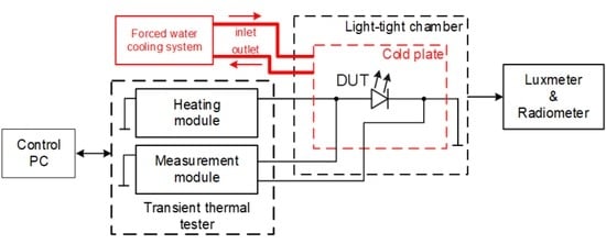
This Section describes the measurement method and the set-up used to obtain characteristics of the tested diodes illustrating an influence of the operating conditions on electric, optical and thermal properties of these devices. All the considered parameters are measured simultaneously with the use of the set-up described below. A view of the considered set-up is shown in Figure 1a. This set-up consists of a transient thermal tester, a water-cooling system with a cold plate, a light-tight chamber, a luxmeter, and a radiometer. The interior of the light-tight chamber with the cold plate are shown in Figure 1b [28]. The cold plate with a tested power LED is placed inside the light-tight chamber. The thermocouple is used to measure the temperature of the cold plate. The block diagram showing the main components of the measurement system is presented in Figure 2.
Tested devices are heated by the transient thermal tester, which is also used to record their dynamic temperature responses, i.e., the variations of the voltage drop across LED junctions in time. When isothermal characteristics are measured, the tested devices, soldered to an MCPCB, are placed on a cold plate. The temperature of the cold plate is stabilized at a preset temperature value by a thermostat forcing liquid flow through the plate. Taking into account that, in the case of power devices, the temperature regulation time might be unacceptably long, the control system response might be accelerated, as demonstrated in [29], owing to the use of Peltier thermoelectric modules inserted between the plate and the PCB. However, if non-isothermal measurements are to be taken in the natural convection cooling conditions, the MCPCB is placed horizontally in thermally insulating clamps. For optical measurements, devices on the cold plate or in the clamp are placed inside the light-tight box and the flux density of emitted light is measured by a radiometer. The operation of the entire measurement system is controlled by a PC where all measurement data are stored.
Thermal resistance was measured with the commercial T3Ster ® equipment manufactured by the MicReD division of Mentor Graphics (Budapest, Hungary) [30]. This equipment is now the industrial standard for device thermal characterization [15] and it realizes the classical pulse measurement method described e.g. in the papers [9]. In this method the tested device is excited by rectangular current pulses. The frequency of this signal is very low, and the duty cycle is close to 1. The user can select the values of low measurement current IL and high heating current IH. The voltage drop values of tested diodes are measured at the low (VL) and high (VH) forward current values.
The device under test was placed on the cold plate, whose temperature value was stabilized by a thermostat. The system for water forced cooling of electronic devices is described in the paper [31]. In order to assure higher thermal conductance, some silicon thermal paste was applied between the cold plate surface and the metal core printed circuit board (MCPCB) on which the tested diodes were mounted. The cold plate temperature Ta was regulated during the experiment over the range from 10 °C to 90 °C.
The measurement equipment is dedicated to thermal parameters of typical semiconductor devices, e.g., p–n diodes, but it does not include instruments making it possible to measure optical parameters of power LEDs. Therefore, it is possible to measure with this system only electric thermal resistance defined in the JEDEC standard [15]. When only electric thermal resistance is measured, the influence of optical power on the results of measurements is neglected.
In order to measure thermal resistance of the considered type of power LEDs, the measurement equipment shown in Figure 1 was used. The thermal resistance Rth is measured using the following formula:
where αT denotes the slope of the thermometric characteristic VL(T) describing the dependence of the diode forward voltage VL on temperature at the forward current equal to IM; VLB and VLE denote the values of the diode forward voltage measured at the current IM when measurements, respectively, start and end; IH and VH denote forward current and forward voltage of the tested diodes during heating process at the steady state, whereas Popt is the optical power emitted by tested device.
The measurements of the surface optical power density were performed using the HD2302 radiometer [32] manufactured by Delta Ohm (Caselle di Selvazzano, Italy). The probe of the radiometer was situated at the distance of 17 cm directly above the light source. The optical power emitted by the investigated diodes was measured using the method presented in [18,33]. This method is based on the measurements of surface density of power of the emitted light by means of the radiometer, the data provided by the diode manufacturer, and the application of some classic geometrical dependencies.
The junction temperature values of the tested diodes at the steady state were measured using the standard pulse electric method [34]. Measurements were performed for different values of LED forward current over a wide range of values of cold plate temperature. The values of diode current ID and voltage VD as well as their junction temperature Tj and the surface power density of the emitted radiation Φe were registered simultaneously.
The electric current-voltage characteristics of the tested LEDs measured at the thermal steady state. The measurements were carried out by measuring thermal resistance. The coordinates of points lying on these characteristics are (VH, IH).
3. Tested Devices
The electric, thermal and optical parameters were measured for two types of power LEDs manufactured by the Cree, Inc. (Durham (North Carolina), USA); XPLAWT-00-0000-000BV50E3 (further on called XPLAWT) and MCE4WT-A2-0000-JE5 (further on called MCE). The values of selected parameters characterising the properties of tested devices are provided in Table 1.
For the diode XPLAWT, the nominal dissipated power of these LEDs amounts to 10 W, the maximum forward current is equal to 3 A, and the luminous flux at the current of 1050 mA is 460 lm [35]. In turn, for the MCE diode the nominal dissipated power amounts to 2.8 W, the maximum forward current is equal to 0.7 A, and the luminous flux at the current of 350 mA is 100 lm [36]. The typical thermal resistance between the junction and the soldering point Rthj-s provided in the datasheets is equal for the considered LEDs to 2.2 K/W and 3 K/W, respectively. The MCE diode contains four independently operating structures, but in our investigations only one of them is powered.
The measurements were taken for the diodes XPLAWT situated on the MCPCBs presented in Figure 3a. These boards have dimensions of 25 mm x 25 mm and the thickness of 2 mm. The package of one diode was soldered to the thermal pad, also shown in the figure, whereas the other one did not use the thermal pad.
On the other hand, the MCE diode is a compound device containing four LED structures, which can be powered independently. In the current investigations only one structure was used. The view of the MCE diode and the layout of the PCB used to assemble this diode are shown in Figure 3b. The dimensions of the MCPCB are 35 mm x 35 mm, and its thickness is equal to 2 mm. The thickness of the dielectric layer is 60 μm. Comparing the MCPCBs used for the assembly of both tested power LEDs, one can observe that their surface areas differ by almost two times. Besides, the shape and the dimensions of thermal pads are also visibly different.
4. Results
Using the measurement method described in Section 2, selected characteristics illustrating electric, optical, and thermal properties of the tested diodes were obtained for these devices operating with soldered thermal pads and non-soldered thermal pads. The electric properties of the considered devices are described by the non-isothermal current-voltage characteristics. The thermal properties are illustrated by the dependencies of thermal resistance on the diode forward current. Finally, the optical properties of these power LEDs are characterized by dependencies of optical power and luminance on the forward current. Moreover, radiant efficiency of the tested power LEDs was calculated. Selected results of these investigations are shown in Figure 4, Figure 5, Figure 6, Figure 7, Figure 8, Figure 9, Figure 10, Figure 11, Figure 12 and Figure 13. In these figures, the solid lines denote the measurement results obtained for the diodes with the thermal pad soldered, and the dashed ones - for the diodes operating without the thermal pad soldered.
Figure 4 presents the non-isothermal current voltage characteristics of the XPLAWT diodes obtained at selected values of temperature of the cold plate Ta, which is equal to temperature of the MCPCB. As it is visible in the figure, an increase in temperature Ta shifts the characteristics to the left. This effect is observed as a result of self-heating, which is more visible for the diode operating without the thermal pad. In this case the increase in the diode internal temperature over the cold plate temperature is higher. For both manners of assembly, the differences in the junction temperature and the forward voltage drop increase with current. On the other hand, an increase in junction temperature at a constant value of forward voltage causes approximately exponential increase of the forward current.
In Figure 4 it is shown that differences in the forward voltage of the diode XPLAWT due to the variation of the device junction temperature Tj between diodes operating with a thermal pad and without it are equal even to 150 mV at the current of 2 A. In turn, the differences in values of junction temperature at the same value of current exceed even 60 °C. The maximum value of junction temperature of the diode operating without a thermal pad is equal to even 145 °C at Ta = 90 °C and ID = 2 A. The temperature coefficient of forward voltage changes with the value of forward current and temperature Ta. At the forward current equal to 2 A and temperature Ta = 10 °C, this coefficient is equal to −2.5 mV/K.
Figure 5 presents for different forward current values the measured diode voltage change ΔVD in response to the variation of the cold plate temperature from 90 °C to 10 °C (ΔTa = −80 °C) in the case of MCE diodes operating with the thermal pad and without it. The value of ΔVD was obtained as the difference of values of forward voltage of the tested LEDs measured at the same value of their forward current and at both above mentioned values of cold pate temperature. As observed, the value of ΔVD is an increasing function of current ID. Due to the self-heating phenomenon, the value of the considered voltage change is higher for the diode operating without the thermal pad. The observed differences between values of ΔVD obtained for both considered mounting methods attain even 60 mV at the current equal to 0.7 A.
Figure 6 illustrates the dependence of the forward voltage of the MCE diode on temperature Ta at two different forward current values. As observed, an increase in temperature of the cold plate causes a decrease in the diode forward voltage. The observed dependence VD(Ta) is non-linear. The values of VD voltage obtained for the diode operating with the thermal pad are lower than for the diode operating without the pad, but the differences between these values decrease with the increase of temperature Ta and with the decrease in forward current ID.
Figure 7 illustrates for different cold plate temperature values the influence of the forward current on the junction temperature of the MCE diodes operating in both types of mounting manner considered here. Obviously, an increase in forward current and the cold plate temperature causes an increase in the junction temperature. It is worth observing that the diode operating with the thermal path has even a 25 °C lower value of junction temperature Tj than the diode of the same type operating without the thermal pad. The influence of the thermal pad on the junction temperature is the most visible for the lowest value of temperature Ta. It can be also observed that an increase in the value of forward current causes a decrease of the difference between values of temperature Tj obtained at different values of temperature Ta. It is a result of a decreasing thermal resistance value of the tested diodes with an increase in the cold plate temperature.
The influence of device mounting manner of the considered diodes on their thermal resistance is illustrated in Figure 8 and Figure 9. In Figure 8, the measured dependences of thermal resistance of the XPLAWT (Figure 8a) and MCE (Figure 8b) diodes on their forward current are shown. The measurements were performed at different values of cold plate temperature. It can be easily noticed that owing to the use of the thermal pad the diode thermal resistance of XPLAWT diode is effectively reduced. Differences in the value of this parameter exceed even 40% for the low value of forward current (100 mA). At higher values of current these differences decrease. For the current equal to 2 A, the value of thermal resistance decreases by less than 30%. For the LED operating without the thermal pad, this decrease is smaller, and it does not exceed 25%.
In practice, the results shown in Figure 8a mean that for the forward current equal to 2 A an excess of the device internal temperature above the ambient temperature is equal to about 90 °C for the LED with the thermal pad and above 130 °C for the LED without the thermal pad, thus demonstrating its importance for the thermal performance of the device. It is also worth noticing that there are no visible differences between the results of measurements obtained for different cold plate temperature values. This proves that in the considered case the value of thermal resistance results mainly from efficiency of heat conduction between the diode junction and the cold plate. The influence of convection and radiation on the thermal resistance value Rth is negligibly small. The rate of heat removal through the cold plate is very high, and it does not depend on the velocity of cooling liquid.
It is visible in Figure 8b that for the MCE diode a strong influence of the cold plate temperature on thermal resistance is observed. In the considered range of temperature variations, the thermal resistance can change by over 30%, and for higher Ta values, thermal resistance Rth is reduced. For the considered diode operating with the thermal pad, an increasing function describes the dependence Rth(ID) for low values of current ID. The influence of this current ID is very weak for the diode operating with the thermal pad, whereas it is very strong for the diode operating without the thermal pad.
Figure 9 presents the dependence of thermal resistance of the MCE diode on the the cold plate temperature. Looking at Figure 9, it is visible that there exists a certain minimum of the thermal resistance Rth at the cold plate temperature value Ta equal to about 50 °C. It is also easy to observe that for the diode operating without the thermal pad the changes in thermal resistance are much bigger than for the diode operating with the pad.
The last part of the presented experimental results illustrates the influence of the thermal pad on the optical parameters of tested power LEDs. The measured surface power density of light emitted by the XPLAWT diode presented in Figure 10 is an increasing function of the diode forward current ID. The increase of the cold plate temperature reduces the emitted light power. Moreover, it is also visible that owing to the use of the thermal pad it is possible to obtain higher values of power density. These differences become more apparent with the increased diode current and exceed even 10%.
Figure 11 shows dependences of a change in the surface power density of the emitted light ΔΦe on forward current for the MCE diode. This change was measured while changing temperature of the cold plate over the range from 10 °C to 90 °C. This change is an increasing function on the diode forward current, and at ID = 0.7 A, it attains even 0.7 W/m2. The changes in the value of Φe obtained for both the considered kinds of mounting the tested power LEDs do not visibly differ between each other, and they are comparable with the measurement error.
In turn, Figure 12 illustrates the dependence of the surface power density of the emitted light on temperature of the cold plate at selected values of forward current. The considered dependence Φe(Ta) is a decreasing function. The slope of this dependences is much higher for the higher of the considered values of the diode forward current. This slope is equal to even −0.225 %/K for ID = 0.7 A, whereas for ID = 0.1 A, this slope is practically equal to zero.
The computed dependences of the efficiency ηopt of the conversion of electrical energy into light in the tested LEDs is shown in Figure 13a for the diode XPLAWT and in Figure 13b for the diode MCE. This efficiency is equal to the quotient of the optical power Popt and the product of the diode current ID, and the diode forward voltage drop across its junction VD. The computed efficiency ηopt, in all cases has a distinct maximum. This maximum is observed at the current equal to about 30 mA for the diode without the thermal pad and around 100 mA for the diode with the thermal pad. Interestingly enough, at lower current values, a higher efficiency of conversion is observed for the diode without the thermal pad. However, within this range of currents, the power of the emitted radiation is relatively small, and junction temperature of the diode is nearly to the cold plate temperature.
Within the range of forward current values typical for the investigated diodes, the use of the thermal pad makes it possible to achieve higher efficiency ηopt and a higher power value of the emitted radiation. The change of the cold plate temperature does not influence in an essential way the relationship between the efficiency values computed for both manners of the diode mounting, since an increase of the cold plate temperature by 80 °C causes the decrease of efficiency by only several percent. It is interesting that the relationship between the characteristics obtained for the MCE diodes operating in different mounting conditions and the cold plate temperature are much different for the XPLAWT diode. Additionally, for the diode with the soldered thermal pad important differences in values of the efficiency ηopt obtained for different Ta values are noticeable. These differences exceed even 7%. For both diodes the maximum value of the efficiency is observed at the ID current in the range from 20 to 50 mA.
In order to compare the influence of thermal pad on properties of the considered power LEDs, some values of parameters of these diodes are collected in Table 2.
The change in forward voltage ΔVD at maximal value of forward current considered here and the change of the cold plate temperature from 10 °C to 90 °C has much smaller values for the diode XPLAWT, but the highest value of ΔVD voltage is observed for the MCE diode without soldered thermal pads. The value of thermal resistance Rth measured for the above mentioned values of forward current ID is much smaller for the tested devices with soldered thermal pad. Differences in values of this parameter exceed even 50% for MCE diode. Consequently, an excess in junction temperature ΔTj of the tested diode at selected value of current ID caused by self-heating phenomenon is much higher for the diode operating without thermal pad.
Finally, the change in surface power density ΔΦe at selected value of the current ID at changing temperature of the cold plate by 80 °C is not big and it does not exceed 5% for both the diodes. Analyzing presented results of measurements, it can be stated that the use of thermal pads makes it possible to reduce visibly the values of thermal resistance and junction temperature of the considered devices, but changes in values of optical and electric parameters are not significant. Consistent with the classic theory of reliability of semiconductor devices [21] and obtained results of measurements, the lifetime of the power LEDs operating with soldered thermal pad can be three times longer than for the same devices operating without the thermal pad.
5. Conclusions
This paper presented the results of measurements illustrating the influence of the thermal pad on electric, thermal and optical parameters of selected power LEDs. As demonstrated, these parameters influence one another. For example, an increase in thermal resistance causes a decrease in electrical power consumed by the considered diodes. In turn, an increase in junction temperature causes a decrease in the density of emitted light flux.
Based on these results, it is clearly visible that the thermal pad considerably reduces thermal resistance of the considered diodes. This reduction is more visible for the diode situated on the larger MCPCBs. For the MCE diode, its thermal resistance is a decreasing function of forward current and cold plate temperature. It was demonstrated that due to differences in the thermal resistance of power LEDs mounted in a different manner, the differences in the junction temperature of these diodes at the same value of forward current can attain even 30 °C. Owing to the more effective cooling of the LED mounted with the thermal pad soldered, it is possible to attain higher power values of the emitted light. This power could be even by 10% higher than for the XPLAWT diode operating without the thermal pad. The observed difference in the power value is an increasing function of the forward current.
Furthermore, it was shown that using the thermal pad results in the increase in the value of the efficiency of the electrical energy conversion into light, especially for higher values of the diode forward current. It was also shown that the increased temperature over the ambient causes the decrease of the conversion efficiency. It is worth pointing out that the efficiency of the tested XPLAWT diodes for low values of forward current exceeded even 80%. Moreover, it is worth noticing that an increase in temperature of the cold plate causes a visible decrease in the diode forward voltage and in the power density of the emitted light. This decrease is the most visible for high forward current values.
The results of performed investigations could be useful for designers of solid-state light sources or substrates dedicated for their applications. Taking into account presented results it might be possible to significantly improve the efficiency and lifetime of the power LEDs used in light sources.
Author Contributions
Conceptualization, K.G. and M.J.; methodology, K.G., P.P., and M.J.; investigation, P.P. and T.T.; writing—original draft preparation, K.G. and M.J.; writing—review and editing, K.G., P.P., and M.J.; visualization, K.G. and P.P.; supervision, K.G. and M.J. All authors have read and agreed to the published version of the manuscript.
Funding
This research was funded by the program of the Ministry of Science and Higher Education called “Regionalna Inicjatywa Doskonałości” in the years 2019–2022, project number 006/RID/2018/19, sum of financing 11 870 000 PLN.
Conflicts of Interest
The authors declare no conflict of interest.
References
- Schubert, E.F. Light Emitting Diodes, 3rd ed.; Rensselaer Polytechnic Institute: Troy, NY, USA, 2018. [Google Scholar]
- Lasance, C.J.M.; Poppe, A. Thermal Management for LED Applications; Springer: Dordrecht, The Netherlands, 2014. [Google Scholar]
- Poppe, A. Multi-domain compact modeling of LEDs: An overview of models and experimental data. Microelectron. J. 2015, 46, 1138–1151. [Google Scholar] [CrossRef]
- Górecki, K. Modelling mutual thermal interactions between power LEDs in SPICE. Microelectron. Reliab. 2015, 55, 389–395. [Google Scholar] [CrossRef]
- Górecki, P.; Górecki, K. Modelling dc Characteristics of the IGBT Module with Thermal Phenomena Taken into Account. In Proceedings of the 13th IEEE International Conference on Compatibility, Power Electronics and Power Engineering IEEE CPE POWERENG 2019, Sonderborg, Denmark, 23–25 April 2019. paper SF-001201. [Google Scholar] [CrossRef]
- Zarębski, J.; Górecki, K. SPICE-aided modelling of dc characteristics of power bipolar transistors with selfheating taken into account. Int. J. Numer. Model. Electron. Netw. Devices Fields 2009, 22, 422–433. [Google Scholar] [CrossRef]
- Górecki, K.; Zarębski, J.; Górecki, P.; Ptak, P. Compact thermal models of semiconductor devices—A review. Int. J. Electron. Telecommun. 2019, 65, 151–158. [Google Scholar] [CrossRef]
- Bagnoli, P.E.; Casarosa, C.; Ciampi, M.; Dallago, E. Thermal resistance analysis by induced transient (TRAIT) method for power electronic devices thermal characterization—part I. Fundamentals and theory. IEEE Trans. Power Electron. 1998, 13, 1208–1219. [Google Scholar] [CrossRef]
- Zhu, H.; Lu, J.; Wu, T.; Guo, Z.; Zhu, L.; Xiao, J.; Gao, Y.; Lin, Y.; Chen, Z. A Bipolar-Pulse Voltage Method for Junction Temperature Measurement of Alternating Current Light-Emitting Diodes. IEEE Trans. Electron Devices 2017, 64, 2326–2329. [Google Scholar] [CrossRef]
- Farkas, G.; Bein, M.C.; Gaal, L. Multi Domain Modelling of Power LEDs Based on Measured Isothermal and Transient I-V-L Characteristics. In Proceedings of the 22nd International Workshop on Thermal Investigations of ICs and Systems Therminic, Budapest, Hungary, 21–23 September 2016; pp. 181–186. [Google Scholar]
- Szekely, V. A new evaluation method of thermal transient measurement results. Microelectron. J. 1997, 28, 277–292. [Google Scholar] [CrossRef]
- Blackburn, D.L. Temperature Measurements of Semiconductor Devices—A Review. In Proceedings of the 20th IEEE Semiconductor Thermal Measurement and Management Symposium SEMI-THERM, San Jose, CA, USA, 11 March 2004; pp. 70–80. [Google Scholar] [CrossRef]
- Górecki, K.; Górecki, P.; Zarębski, J. Measurements of parameters of the thermal model of the IGBT module. IEEE Trans. Instrum. Meas. 2019, 68, 4864–4875. [Google Scholar] [CrossRef]
- Górecki, K.; Zarębski, J. Modelling the influence of selected factors on thermal resistance of semiconductor devices. IEEE Trans. Component. Packag. Manuf. Technol. 2014, 4, 421–428. [Google Scholar] [CrossRef]
- JEDEC Standard JESD51-51. Implementation of Electrical Test Method for the Measurement of Light-Emitting Diodes. 2012. Available online: https://www.jedec.org/sites/default/files/docs/JESD51-52.pdf (accessed on 18 July 2020).
- Górecki, K.; Ptak, P. New method of measurements transient thermal impedance and radial power of power LEDs. IEEE Trans. Instrum. Meas. 2020, 69, 212–220. [Google Scholar] [CrossRef]
- Górecki, K.; Dziurdzia, B.; Ptak, P. The influence of a soldering manner on thermal properties of LED modules. Solder. Surf. Mt. Technol. 2018, 30, 81–86. [Google Scholar] [CrossRef]
- Górecki, K.; Ptak, P.; Janicki, M.; Torzewicz, T. Influence of Cooling Conditions of Power LEDs on Their Electrical, Thermal and Optical Parameters. In Proceedings of the 25th International Conference Mixed Design of Integrated Circuits and Systems MIXDES 2018, Gdynia, Poland, 21–23 June 2018; pp. 237–242. [Google Scholar]
- Torzewicz, T.; Ptak, P.; Górecki, K.; Janicki, M. Influence of LED Operating Point and Cooling Conditions on Compact Thermal Model Element Values. In Proceedings of the 24th International Workshop on Thermal Investigastions of ICs and Systems Therminic, Sztokholm, Sweden, 26–28 September 2018. [Google Scholar] [CrossRef]
- Górecki, K.; Ptak, P. The influence of the Mounting Manner of the Power LEDs on Its Thermal and Optical Parameters. In Proceedings of the 21st International Conference Mixed Design of Integrated Circuits and Systems MIXDES, Lublin, Poland, 19–21 June 2014; pp. 303–308. [Google Scholar]
- Narendran, N.; Gu, Y. Life of LED-based white light sources. J. Disp. Technol. 2005, 1, 167–171. [Google Scholar] [CrossRef]
- Castellazzi, A.; Gerstenmaier, Y.C.; Kraus, R.; Wachutka, G.K.M. Reliability analysis and modeling of power MOSFETs in the 42-V-PowerNet. IEEE Trans. Power Electron. 2006, 21, 603–612. [Google Scholar] [CrossRef] [Green Version]
- Górecki, P.; Górecki, K.; Kisiel, R.; Myśliwiec, M. Thermal parameters of monocrystalline GaN Schottky diodes. IEEE Trans. Electron. Devices 2019, 66, 2132–2138. [Google Scholar] [CrossRef]
- Dziurdzia, B.; Górecki, K.; Ptak, P. Influence of a soldering process on thermal parameters of large power LED modules. IEEE Trans. Componen. Packag. Manuf. Technol. 2019, 9, 2160–2167. [Google Scholar] [CrossRef]
- Skwarek, A.; Ptak, P.; Górecki, K.; Hurtony, T.; Illes, B. Microstructure influence of SACX0307-TiO2 composite solder joints on thermal properties of power LED assemblies. Materials 2020, 13, 1563. [Google Scholar] [CrossRef] [PubMed]
- Górecki, K.; Ptak, P. Modelling LED lamps in SPICE with thermal phenomena taken into account. Microelectron. Reliab. 2017, 79, 440–447. [Google Scholar] [CrossRef]
- Górecki, K.; Ptak, P.; Torzewicz, T.; Janicki, M. Influence of the Use of A Thermal Pad on Electric, Optical and Thermal Parameters of Selected Power LEDs. In Proceedings of the 25th International Workshop on thermal Investigations of ICs and Systems Therminic 2019, Lecco, Italy, 25–27 September 2019. [Google Scholar] [CrossRef]
- Janicki, M.; Torzewicz, T.; Ptak, P.; Raszkowski, T.; Samson, A.; Górecki, K. Parametric compact thermal models of power LEDs. Energies 2019, 12, 1724. [Google Scholar] [CrossRef] [Green Version]
- Janicki, M.; Kulesza, Z.; Torzewicz, T.; Napieralski, A. Automated Stand for Thermal Characterization of Electronic Packages. In Proceedings of the 27th Annual IEEE Semiconductor Thermal Measurement and Management Symposium Semi-Therm, San Jose, CA, USA, 20–24 March 2011; pp. 199–202. [Google Scholar] [CrossRef]
- Datasheet T3Ster Equipment. Available online: https://corner-stone.com.tw/wp-content/uploads/2017/06/T3ster-technical-information.1.pdf (accessed on 18 June 2020).
- Datasheet Thermal Scientific Fisher Haake A25. Available online: https://pim-resources.coleparmer.com/instruction-manual/12135-xx.pdf (accessed on 18 June 2020).
- Datasheet DeltaOhm HD2302. Available online: http://www.otm.sg/files/HD2302_M_uk.pdf (accessed on 20 March 2020).
- Górecki, K.; Ptak, P. New dynamic electro-thermo-optical model of power LEDs. Microelectron. Reliab. 2018, 91, 1–7. [Google Scholar] [CrossRef]
- Blackburn, D.L.; Oettinger, F.F. Transient thermal response measurements of power transistors. IEEE Trans. Ind. Electron. Control. Instrum. 1976, IECI-22, 134–141. [Google Scholar] [CrossRef]
- Datasheet Cree XPLAWT-00-0000-000BV50E3. Available online: https://www.cree.com/led-components/media/documents/ds-XPL.pdf (accessed on 18 June 2020).
- Datasheet Cree MCE4WT-A2-0000-JE5. Available online: https://www.cree.com/led-components/media/documents/XLampMCE.pdf (accessed on 18 June 2020).
Figure 1.
(a) View of the measurement equipment; (b) the interior of the light-tight chamber with the cold plate and a power LED [29].
Figure 1.
(a) View of the measurement equipment; (b) the interior of the light-tight chamber with the cold plate and a power LED [29].

Figure 2.
Block diagram of the measurement set-up.

Figure 3.
(a) View of the metal core printed circuit board (MCPCB) with the XPLAWT LED and the view of this LED electrode layout for this LED; (b) view of the MCE LED soldered to the MCPCB and the layout of this MCPCB.
Figure 3.
(a) View of the metal core printed circuit board (MCPCB) with the XPLAWT LED and the view of this LED electrode layout for this LED; (b) view of the MCE LED soldered to the MCPCB and the layout of this MCPCB.

Figure 4.
Measured DC I-V characteristics of the XPLAWT diodes at selected values of cold plate temperature.
Figure 4.
Measured DC I-V characteristics of the XPLAWT diodes at selected values of cold plate temperature.

Figure 5.
Measured MCE diode forward voltage change ΔVD in response to the cold plate variation by 80 °C in function of the diode forward current.
Figure 5.
Measured MCE diode forward voltage change ΔVD in response to the cold plate variation by 80 °C in function of the diode forward current.

Figure 6.
Measured dependences of the forward voltage of MCE diodes on the cold plate temperature for different forward current values.
Figure 6.
Measured dependences of the forward voltage of MCE diodes on the cold plate temperature for different forward current values.

Figure 7.
Measured dependences of the junction temperature of the MCE diodes on forward current for different values of the cold plate temperature.
Figure 7.
Measured dependences of the junction temperature of the MCE diodes on forward current for different values of the cold plate temperature.

Figure 8.
Measured dependences of thermal resistance on forward current for different cold plate temperature values for: (a) the XPLAWT; (b) MCE diode.
Figure 8.
Measured dependences of thermal resistance on forward current for different cold plate temperature values for: (a) the XPLAWT; (b) MCE diode.

Figure 9.
Measured dependences of thermal resistance of the MCE diode on the cold plate temperature for different forward current values.
Figure 9.
Measured dependences of thermal resistance of the MCE diode on the cold plate temperature for different forward current values.

Figure 10.
Measured dependences of the surface power density of light emitted by the XPLAWT diode on the LED forward current for different cold plate temperature values.
Figure 10.
Measured dependences of the surface power density of light emitted by the XPLAWT diode on the LED forward current for different cold plate temperature values.

Figure 11.
Measured dependences of the surface power density change ΔΦe of the diodes MCE on forward current.
Figure 11.
Measured dependences of the surface power density change ΔΦe of the diodes MCE on forward current.

Figure 12.
Measured dependences of the surface power density Φe of the diodes MCE on temperature of the cold plate.
Figure 12.
Measured dependences of the surface power density Φe of the diodes MCE on temperature of the cold plate.

Figure 13.
Measured dependences of radiant efficiency on the forward current for different cold plate temperature values for: (a) the XPLAWT; (b) MCE diodes.
Figure 13.
Measured dependences of radiant efficiency on the forward current for different cold plate temperature values for: (a) the XPLAWT; (b) MCE diodes.


Table 1.
The values of the operating parameters of the tested LEDs.
| Diode | IDmax [A] | PD [W] | VF [V] | Tjmax [°C] | Viewing Angle [°] | Rth j-s [K/W] | ɸV [lm] |
|---|---|---|---|---|---|---|---|
| XPLAWT | 3 | 10 | [email protected] | 150 | 125 | 2.2 | [email protected] |
| MCE | 0.7 | 2.8 | [email protected] | 150 | 110 | 3 | [email protected] |
Table 2.
The values of selected electric, optical and thermal parameters of the tested power LEDs operating with soldered (WTP) or not soldered (NTP) thermal pads.
Table 2.
The values of selected electric, optical and thermal parameters of the tested power LEDs operating with soldered (WTP) or not soldered (NTP) thermal pads.
| Diode | Thermal Pad | ΔVD@ID | Rth@ID | ΔTj@ID | ΔΦe@ID |
|---|---|---|---|---|---|
| XPLAWT | NTP | 0.159 V@2 A | 20.5 K/W@2 A | 58.4 K@2 A | 3.25 W/m2@2 A |
| WTP | 0.182 V@2 A | 12.3 K/W@2 A | 34.2 K@2 A | 3.09 W/m2@2 A | |
| MCE | NTP | 0.312 [email protected] A | 20.4 K/W@1 A | 37.2 [email protected] A | 0.72 W/m2@0.7 A |
| WTP | 0.251 [email protected] A | 10 K/W@1 A | 27.5 [email protected] A | 0.75 W/m2@0.7 A |
© 2020 by the authors. Licensee MDPI, Basel, Switzerland. This article is an open access article distributed under the terms and conditions of the Creative Commons Attribution (CC BY) license (http://creativecommons.org/licenses/by/4.0/).
Share and Cite
MDPI and ACS Style
Górecki, K.; Ptak, P.; Torzewicz, T.; Janicki, M. Influence of a Thermal Pad on Selected Parameters of Power LEDs. Energies 2020, 13, 3732. https://0-doi-org.brum.beds.ac.uk/10.3390/en13143732
AMA Style
Górecki K, Ptak P, Torzewicz T, Janicki M. Influence of a Thermal Pad on Selected Parameters of Power LEDs. Energies. 2020; 13(14):3732. https://0-doi-org.brum.beds.ac.uk/10.3390/en13143732
Chicago/Turabian StyleGórecki, Krzysztof, Przemysław Ptak, Tomasz Torzewicz, and Marcin Janicki. 2020. "Influence of a Thermal Pad on Selected Parameters of Power LEDs" Energies 13, no. 14: 3732. https://0-doi-org.brum.beds.ac.uk/10.3390/en13143732
Note that from the first issue of 2016, this journal uses article numbers instead of page numbers. See further details here.