Article

An Impedance Network-Based Three Level Quasi Neutral Point Clamped Inverter with High Voltage Gain

1
Department of Electrical Engineering, The University of Lahore, Lahore 54000, Pakistan
2
Marine Engineering Technology Department in a Joint Appointment with the Electrical and Computer Engineering Department, Texas A&M University, Galveston, TX 77554, USA
3
Department of Electrical Engineering, College of Engineering, Majmaah University, Al-Majmaah 11952, Saudi Arabia
4
Department of Electrical Engineering, University of the Punjab, Lahore 54590, Pakistan
5
Department of Electrical Engineering, UAE University, Al-Ain 64141, UAE
*
Authors to whom correspondence should be addressed.
Submission received: 27 December 2019 / Revised: 17 February 2020 / Accepted: 28 February 2020 / Published: 9 March 2020

Abstract

:
Due to the impediments of voltage source inverter and current source inverter, Z-Source Inverter (ZSI) has become notorious for better power quality in low and medium power applications. Several modifications are proposed for impedance source in the form of Quasi Z-Source Inverter (QZSI) and Neutral Point Clamped Z-Source Inverter (NPCZSI). However, due to the discontinuity of the source current, NPCZSI is not suitable for some applications, i.e., fuel cell, UPS, and hybrid electric vehicles. Although in later advancements, source current becomes continuous in multilevel QZSI, low voltage gain, higher shoot-through duty ratio, lesser availability of modulation index, and higher voltage stress across switches are still an obstacle in NPCZSI. In this research work, a three-level high voltage gain Neutral Point Clamped Inverter (NPCI) that gives three-level AC output in a single stage, is proposed to boost up the DC voltage at the desired level. At the same time, it detains all the merits of previous topologies of three-level NPCZSI/QZSI. Simulations have been done in the MATLAB/Simulink environment to show the effectiveness of the proposed inverter topology.

1. Introduction

Z-source inverter (ZSI) has the capability for buck/boost operation; this unique feature is not available in a traditional Current Source Inverter (CSI) and Voltage Source Inverter (VSI). Regardless of this unique feature, Z-source inverter has some curtailments such as lower voltage gain, discontinuous current, and high voltage stresses across the switches [1,2,3]. In the previous literature, several topologies in the form of Quasi Z-Source Inverter (QZSI), Neutral Point Clamped Z-Source Inverter (NPCZSI), and Neutral Point Clamped Quasi Z-Source (NPCQZSI) Inverter were presented to overcome these limitations. For instance, a voltage doubler, in conjunction with an isolation transformer, was utilized in [4] for quasi ZSI for distributed generation applications. Although the topology ensures the continuity in the input current, it offers a limited boosting ability. Theoretical results for four topologies of QZSI inverter having less element count and simplified control techniques were presented in [5,6]. The topologies ensure a continuous current without including a major advancement in boosting ability and voltage stresses across switches. A traditional ZSI integrated with a bridge rectifier was proposed in [7] for adjustable speed drive applications. A QZSI was proposed in [8] that included two inductors, two capacitors, and one diode in the QZS network. This topology offers continuity in the input current, however, with the same boosting ability as that of the traditional ZSI. To increase the modulation index range with the continuity in current, a switched inductor QZSI was proposed in [9]. No drastic increase in the boost factor of the inverter was observed. By utilizing a predictive control method, a grid-connected closed-loop QZSI topology was introduced [10] that claimed an improvement in the inverter performance with the same boosting ability as that of traditional ZSI and high voltage stresses across switches. Similarly, different ZS networks integrated with VSI and CSI were investigated in [11]. These are indeed different topologies with the same boost factor as that of traditional ZSI. To make a smoother DC input current, a family of embedded ZSI was suggested with the traditional boosting ability and high stresses across switches [12]. In all the aforementioned references, improvement in boosting ability is still a challenge.
In [13,14], a three-level NPCZSI was proposed that deployed the two conventional impedance sources that included four capacitors and four inductors with two separate dc sources. This proposed topology of the inverter provides an additional state (0 V) in the output voltage to yield the staircase waveform and reduces the harmonic distortion in output voltage. Due to the deployment of two separate impedance sources, the design of this topology becomes very bulky; additionally, the voltage gain of the inverter does not increase too much. This limitation was addressed in [15], where a single impedance source was deputed with the NPCI to reduce the cost and volume of the inverter while retaining all the advantages of the previous topology.
To achieve the optimal results from NPCZSI in the form of enhanced output voltage, waveform quality, and boosting ability, a detailed comparison between two modulation techniques, Phase Disposition Sinusoidal Pulse Width Modulation (PDSPWM) and Phase Opposite Disposition Sinusoidal Pulse Width Modulation (PODSPWM) were analyzed in [16]. A continuous model was suggested in [17] to balance the voltage between two capacitors in NPCI. Instead of standard inductors, the use of coupled transformers was introduced in [18] to enhance the voltage gain ability of NPCZSI by adjusting the turns ratio of transformers. It also overcomes the dependence on modulation index, and hence, makes the stresses lower across switches. However, with this topology, a colossal rise in voltage gain is restricted due to the shoot-through duty ratio and turns ratio of coupled transformers affecting each other. Said constraint is addressed in [19] by modifying the impedance network with the deployment of coupled inductors. A Coupled Quasi Z-Source Inverter (CQZSI) is suggested in [20] to diminish the input current ripples. A single-phase five-level hybrid NPCI was proposed in [21], which integrated the NPCI with an H-bridge inverter. The proposed inverter contends the accomplishment to lower the total harmonic distortion (THD) through the Selective Harmonic Elimination (SHE) technique.
An NPCI, with a Z-source, that was composed of two diodes, two inductors, two switches, and two capacitors was suggested in [22] that acquired all the benefits of QZSI and provided the three-level output voltages, but due to its lower voltage gain ability, it was not an appropriate choice where a higher boost was required. In [23], two topologies named Diode Assisted QZSI and Capacitor Assisted QZSI were proposed, which were extendable, but the repetition of a greater number of units increased the size of the inverter and made it bulky. From the invention of ZSI [24], a lot of attempts have been made to ameliorate this topology to accomplish the optimal benefits from it, but a small voltage gain, lower value of modulation index, and higher voltage stress are still present in previous topologies suggested in the literature.
This research work introduces a new topology for ZSI that overcomes the drawbacks such as lower boosting ability, utilization of higher shoot-through duty ratio, lesser availability of modulation index, and higher voltage stresses across switches of the previous topologies. This topology offers a remarkable boosting ability and provides a high voltage gain by utilizing a lower shoot-through ratio to make available a higher modulation index and keeps the lower stress across switches.
The paper is organized in the following way. The proposed inverter topology is presented in Section 2, with its complete working modes of operation. A detailed mathematical analysis is performed in Section 3. Section 4 covers the PWM technique, and the Boost Control Method applied to the proposed topology. Simulations and results are provided in Section 5, whereas Section 6 presents a detailed comparison with the previous topologies. Section 7 includes the conclusion.

2. The Proposed Inverter Topology

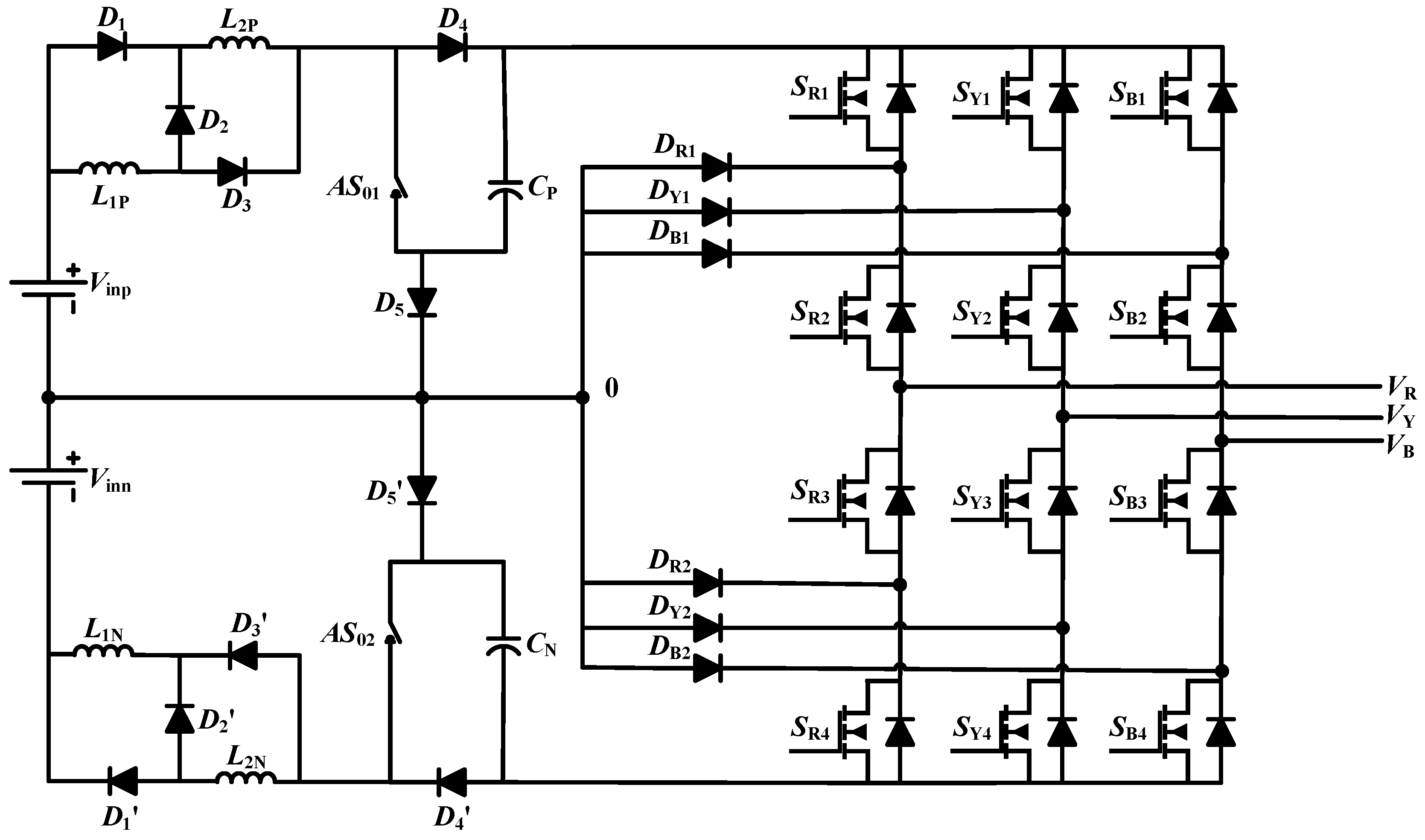
The schematic diagram of the proposed inverter topology, which can enhance the applied DC voltage to the desired level and transform it into a three-phase three-level output, is illustrated in Figure 1. The applied DC voltage can be procured from a DC battery or some other DC source such as a fuel cell or PV applications.
The inverter is configured with two symmetrical impedance networks, where each network is comprised of two inductors, two capacitors, four diodes, and one active switch to provide the numerous advantages over the conventional inverters. Two alike dc sources are utilized to energize these networks. The conventional NPCI [25] can operate only in two types of states, active-states, and zero-states. However, the proposed inverter includes one more state of operation that is a Shoot Through (ST) state (that allows all switches to turn on at a time).
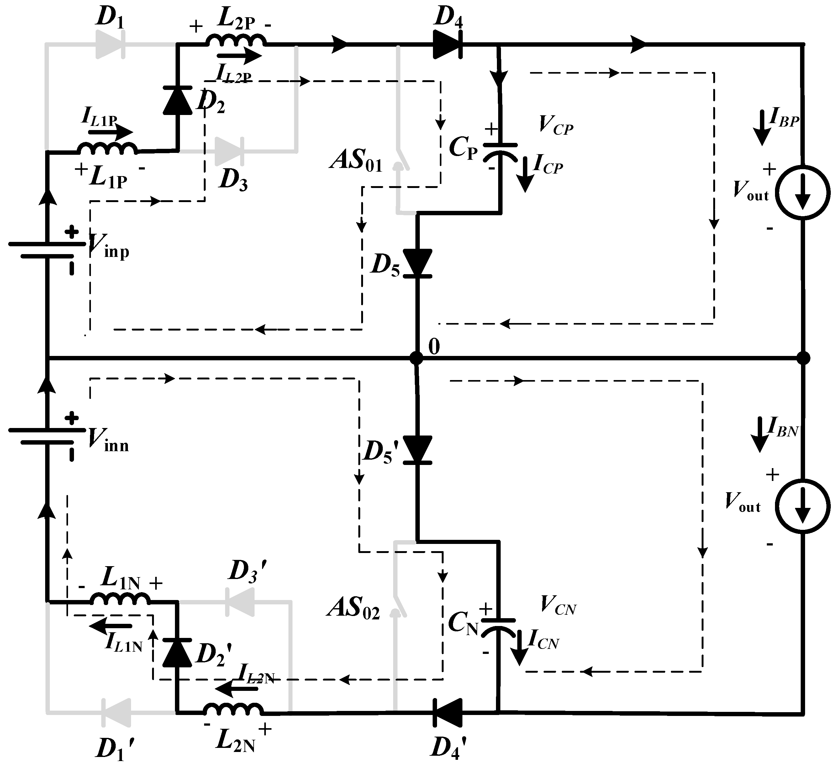
2.1. Active State

Here, the DC voltage applied to the inverter is exposed to the three-phase AC load after conversion to a three-phase three-level AC, at the desired level. In this mode of operation, + V dc or V dc voltage appear at the poles of the inverter.
To achieve + V dc , diodes D 2 and D 4 operate in the conduction mode and D 1 and D 3 remain in the nonconduction mode; L 1 P and L 2 P come in series. DC source V inp and both inductors L 1 P and L 2 P of the upper impedance network energize the capacitor C P . The direction of the current is shown in the equivalent circuit of the active state in Figure 2. In the active state, the current adopts the two paths, one from voltage source V inp to inductor L 1 P , diode D 2 , inductor L 2 P , diode D 4 , and capacitor C P , and completes its path through D 5 . In this path, capacitor C P is charged by voltage source V inp and by inductors L 1 P and L 2 P , while in the second path, the current approaches to ac load after passing through L 1 P , D 2 , L 2 P , S K 1 , S K 2 (where K = R, Y, B) and completes its path through the load to neutral point N and back to V inp .
To achieve V dc , diodes D 2 and D 4 are in conduction mode, while D 1 and D 3 remain in nonconduction mode. DC source voltage V i n n and both inductors L 1 N and L 2 N of lower impedance network energize the capacitor C N . The direction of the flow of current is shown in the equivalent circuit of the active state in Figure 2. In the active state, the current follows the two paths, one from voltage source V i n n to capacitor C N through D 5 and completes its path after passing through inductor L 2 N , diode D 2 , and inductor L 1 N . In this path, the capacitor is charged by voltage source V inn and by inductors L 1 N and L 2 N . In the second path, the current approaches to AC load after passing through S K 3 and S K 4 (where K = R, Y, B), and completes its path through the inductor L2N, diode D 2 , inductor L 1 N , and back to V i n n . In the active state, both active switches ( A S 01 and A S 02 ) remain in off state and play no role.
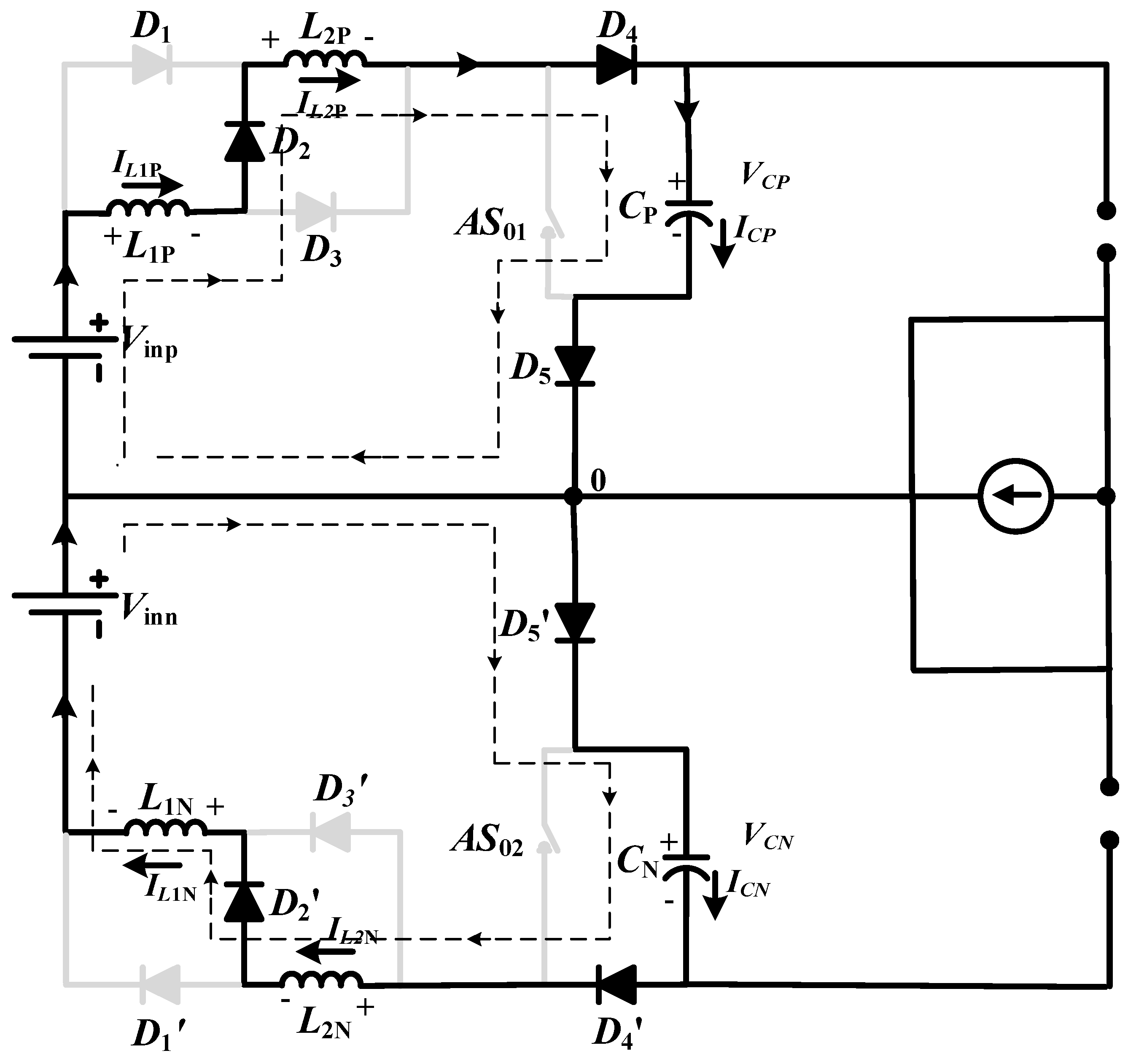
2.2. Zero-State

During the zero-state of operation, no voltage appears across the load terminals. In the zero-state, two intermediate switches of each leg of the inverter are in on state, whereas the topmost and lowermost switch of each leg of the inverter remains in the off state. During this mode of operation, the diodes D 2 and D 4 are in the conduction mode, while D 1 and D 3 remain in the nonconduction mode. DC source V i n p and both inductors L 1 P and L 2 P of the upper impedance network energize the capacitor C P . Similarly, for the lower network, the diodes D 2 and D 4 are in conduction mode, while D 1 and D 3 remain in nonconduction mode and DC source V i n n and both inductors L 1 N and L 2 N of lower impedance network energize the capacitor C N .
The direction of the flow of current in the equivalent circuit of zero-state is shown in Figure 3, where it traverses voltage source V inp , inductor L 1 P , diode D 2 , inductor L 2 P , and capacitor C P and reaches back to V inp through diode D 4 . In this path, capacitor C P is charged by V inp and by both inductors L 1 N and L 2 N . Similarly, for the lower network capacitor, C N is charged by V i n n and by the combination of L 1 N and L 2 N , no power is transferred to load. Like in the active state, both A S 01 and A S 02 remain in off state.

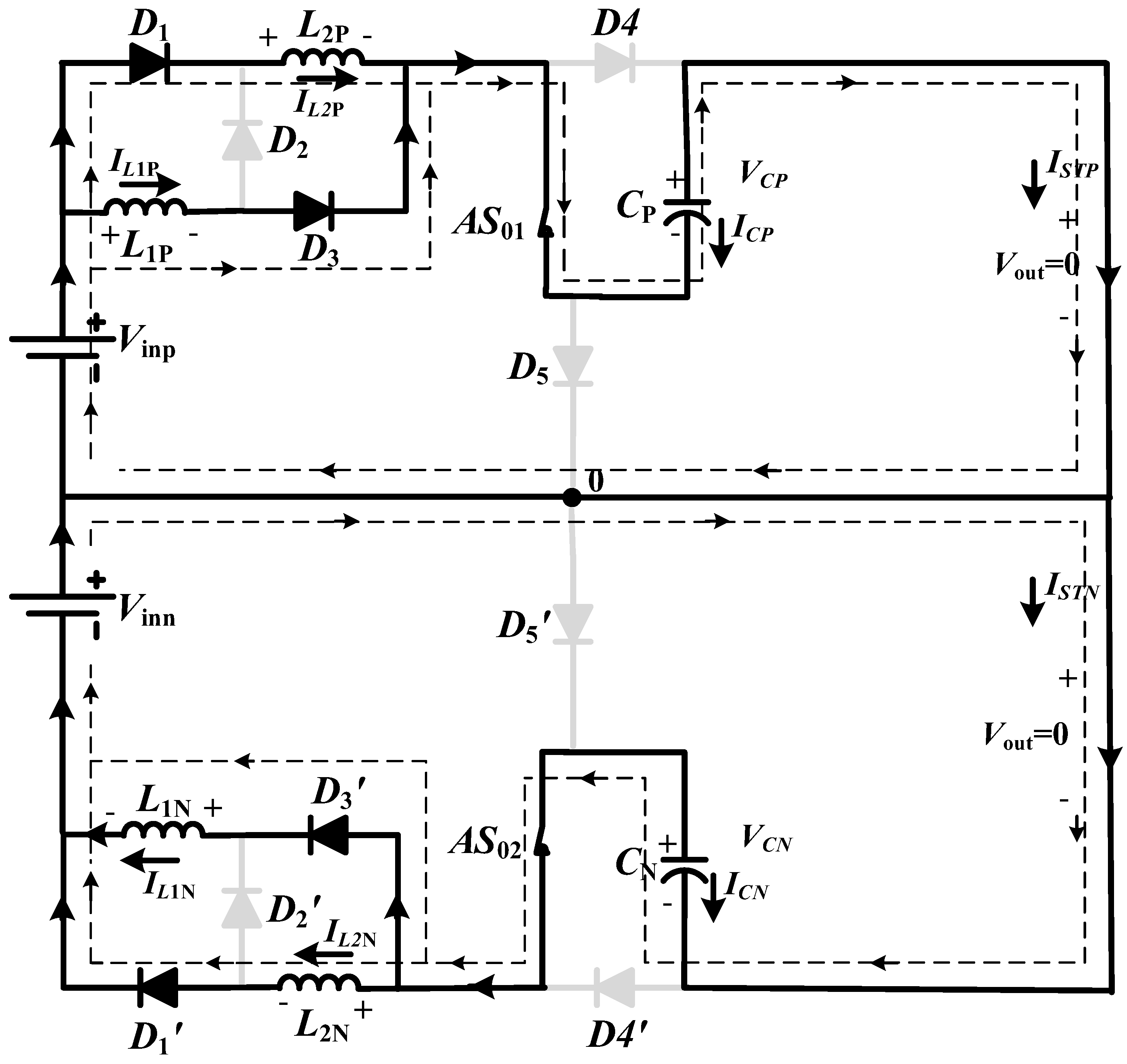
2.3. Shoot-Through (ST) State

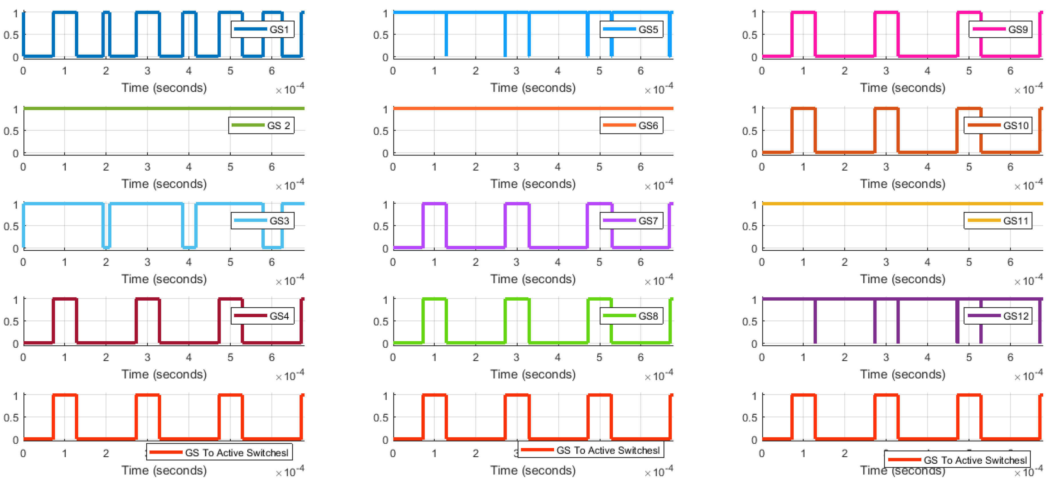
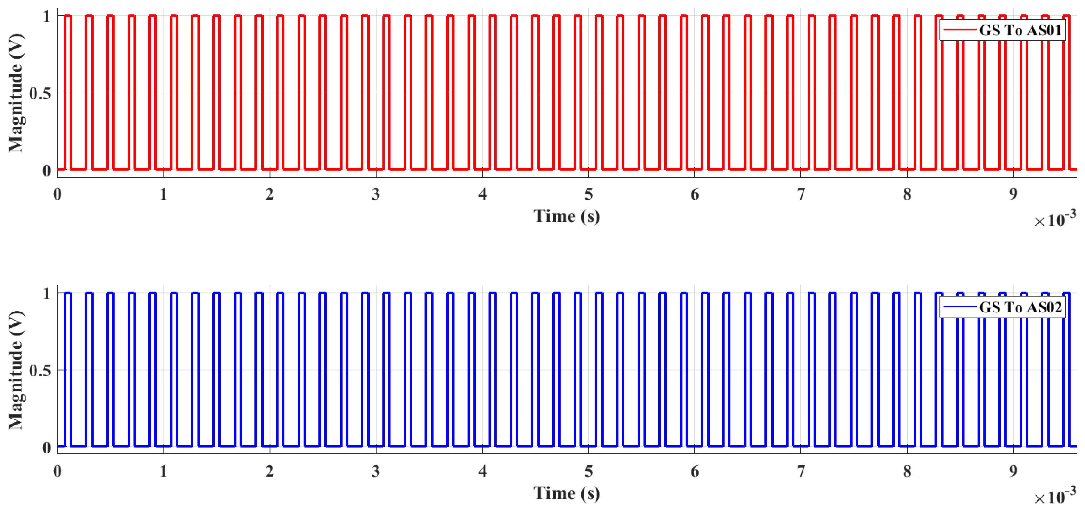
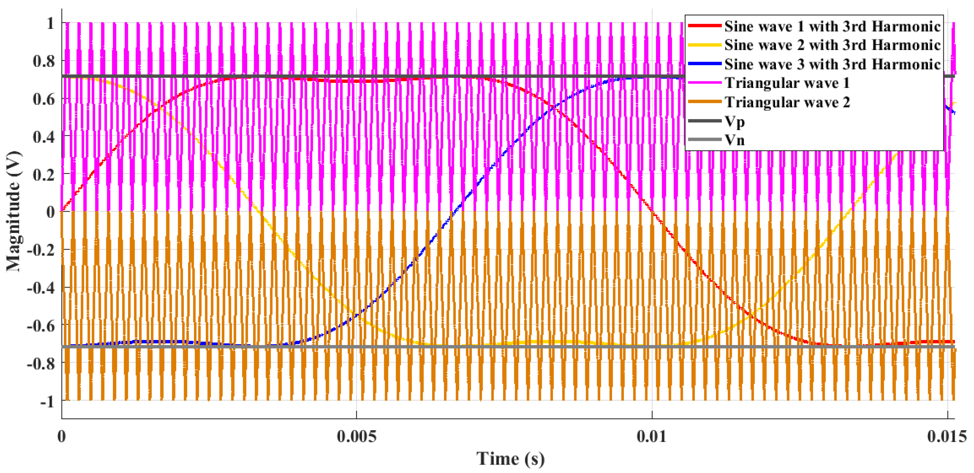
In ST state, active switches, along with all switches of one or more legs of an inverter, go to on state simultaneously, which elicits 0 V across the load (see Figure 4). Seven different approaches that are summarized in Table 1 can be adopted to attain this state.
On closing the active switches, inductors L 1 P and L 2 P come in parallel in the upper impedance network and turns diodes D 2 , D 4 , and D 5 in reverse bias mode. Similarly, L 1 N and L 2 N come in parallel in the lower impedance network and configure diodes D 2 , D 4 , and D 5 in reverse bias mode. In ST state, V inp and capacitor C P charge inductors L 1 P and L 2 P ; similarly, in the lower network, V i n n and capacitor C N charge inductors L 1 N and L 2 N .
The span of the ST state is limited up to the premises of zero-state and is maximum when it occupies the time duration of the zero-state. This state enables the inverter to perform the buck/boost operation. Thus, by choosing its appropriate value, desired results can be achieved.

3. Mathematical Analysis of the Proposed Inverter Topology

In this section, we perform the necessary mathematical calculations for the proposed inverter topology.

3.1. Non-ST-State

Applying the Kirchhoff’s Voltage Law (KVL) to Figure 2, the voltage across inductors L 1 P and L 2 P are:
{ V L 1 P = V inp V CP V L 2 P V L 2 P = V inp V CP V L 1 P
where:
V inp = V L 1 P + V L 2 P + V CP
V CP = V out
To find the inductor and capacitor currents during the non-ST state, apply the Kirchhoff’s Current Law (KCL) on upper impedance network:
I L 1 P = I L 2 P = I CP + I BP
I CP = I L 1 P I BP
or:
I CP = I L 2 P I BP
Similarly, for the lower network during the non-ST state:
{ V L 1 N = V inn V CN V L 2 N V L 2 N = V inn V CN V L 1 N
where:
V inn = V L 1 N + V L 2 N + V CN
V out = V CN
Furthermore, the inductor and capacitor currents are:
I L 1 N = I L 2 N = I CN + I BN
I CN = I L 1 N I BN
or:
I CN = I L 2 N I BN

3.2. ST-State

Apply KVL to Figure 4, the voltage across the inductors L 1 P and L 2 P are given as:
V L 1 P = V L 2 P = V inp + V CP
V out = 0
For inductor and capacitor currents during the ST state, apply the KCL on upper impedance network:
I STP = I L 1 P + I L 2 P = I CP
or:
I CP = ( I L 1 P + I L 2 P ) = I S T P
V L 1 N = V L 2 N = V inn + V CN ,   V out = 0
I STN = I L 1 N + I L 2 N = I CN
or:
I CN = ( I L 1 N + I L 2 N ) = I S T N

3.3. Calculations of Current, Voltage, Boost Factor and Gain Factor

As per the Volt-Second Balance Principle (VSBP), the net voltage across the inductor remains zero during a period of one switching cycle. Apply the VSBP at upper impedance network across both inductors L 1 P and L 2 P during a complete switching time period T osc :
( V inp V CP V L 2 P ) ( 1 D ) T osc + ( V inp + V CP ) D T osc = 0
( V inp V CP V L 1 P ) ( 1 D ) T osc + ( V inp + V CP ) D T osc = 0
Solve (17) to find out the voltage across inductor L 2 P during the non-shoot-through state as:
V L 2 P = V inp + V CP ( 2 D 1 ) ( 1 D )     = V inp ( 1 D ) + V CP ( 2 D 1 ) ( 1 D )
Put the above value V L 2 P into (18):
( V inp ( 1 D ) + V CP ( 2 D 1 ) ( 1 D ) ) ( 1 D ) T osc + ( V inp + V CP ) D T osc = 0
By solving (20), the voltage across capacitor C P is given as:
V CP = V inp ( D + 1 ) 1 3 D
Similarly, apply the VSBP in lower impedance network across inductors L 1 N and L 2 N during a complete switching time period T o s c :
( V inn V CN V L 2 N ) ( 1 D ) T osc + ( V inn + V CN ) D T osc = 0
( V inn V CN V L 1 N ) ( 1 D ) T osc + ( V inn + V CN ) D T osc = 0
After solving (22) and (23), the voltage across capacitor C N is given as:
V CN = V inn ( D + 1 ) 1 3 D
As both the dc input sources are identical V inp = V i n n = V IN , (21) and (24) can be re-written in a general form:
V CP = V CN = V IN ( D + 1 ) 1 3 D
As per the Ampere Second Balance Principle (ASBP), the net current through the capacitor remains zero during a period of one switching cycle. Apply the ASBP to capacitor C P in the upper network to find out the current through both inductors L 1 P and L 2 P :
( I L 1 P I IBP ) ( 1 D ) T osc ( I L 1 P + I L 2 P ) D T osc = 0
( I L 2 P I IBP ) ( 1 D ) T osc ( I L 1 P + I L 2 P ) D T osc = 0
Similarly, for the lower network, apply the ASBP to capacitor C N to find out the current through both inductors L 1 N and L 2 N :
( I L 1 N I IBN ) ( 1 D ) T osc ( I L 1 N + I L 2 N ) D T osc = 0
( I L 2 N I IBN ) ( 1 D ) T osc ( I L 1 N + I L 2 N ) D T osc = 0
Solve (26) and (27), the average current through L 1 P and L 2 P is:
I L 1 P = I L 2 P = ( 1 D ) I IBP ( 1 3 D )
Similarly, the current through inductors L 1 N and L 2 N is found as:
I L 1 N = I L 2 N = ( 1 D ) I IBN ( 1 3 D )
The boost factor B is given as:
B = V out V inp = V CP V inp = V out V inn = V CN V inn
or:
B = ( D + 1 ) 1 3 D
The overall gain factor G for the proposed inverter topology is given as:
G = B M = ( D + 1 ) M 1 3 D
This completes the mathematical calculations for the proposed inverter topology.

4. PWM and Boost Control Techniques

4.1. PWM Signals

The proposed topology is designed for the three-phase three-level inverter; thus, three sine waves with a phase difference of 120 degrees are utilized in the PODSPWM technique [26,27,28,29,30], to generate the Gating Signals (GS) for 12 switches used in the main inverter circuit. The simulation model of the proposed inverter topology is carried out with a 50 Hz frequency for each sinusoidal signal, and the frequency of each triangular signal is kept at 5 kHz. GS for switches in the main inverter circuit is shown in Figure 5.
The GS applied to active switches in the impedance network are illustrated in Figure 6.

4.2. Maximum Constant Boost Control Method (MCBCM)

Although the Maximum Boost Control Method [31] provides a higher value of G with a smaller value of stress across switches Vs; however, due to diversity in the value of D for each switching cycle, it generates the low-frequency ripples in inductor current, which is not desirable [32]. To overcome this situation, and to achieve a higher value of G at lower values of Vs, MCBCM was introduced to provide a constant value of D by using two envelope signals V P and V N . Here, the third harmonic component with a magnitude of 1/6 of the fundamental component is dumped with the sine waves to enhance the range of M . The value of D is given as [32]:
D = ( 2 3 M 2 ) = 1 3 M 2
The value of M can be increased up to 2 / 3 . An increase in the range of M causes a reduction in V S [32]. Due to the numerous advantages of MCBCM over the other boost control methods, MCBCM with PODSPWM is utilized in the Simulink model. The situation is depicted in Figure 7.
The boost factor, overall voltage gain, and stress across the switches for the proposed inverter topology are given as:
B = 4 3 M 3 3 M 4
G = M ( 4 3 M ) 3 3 M 4
V S = B V I N = ( 4 3 M ) V I N 3 3 M 4

5. Simulations Results and Discussion

For solid validation of proposed topology, the inverter is simulated with a detailed switching model in discrete time simulations by using the SimPowerSystems toolbox in MATLAB/Simulink, where the conducting and switching losses are considered for the components used in the impedance network and the main inverter circuit. All the simulation results have a strong agreement with the theoretical results. The details of all components and parameters used in the simulation model for the proposed inverter topology are provided in Table 2 and Table 3.
The proposed topology outperforms the previous techniques and provides an excellent boosting capacity at a very low ST duty ratio with the high modulation index. Table 4 shows the values of the boosting factor against the different values of the ST duty ratio and modulation index.
Detailed simulation results are presented from Figure 8, Figure 9, Figure 10, Figure 11, Figure 12 and Figure 13. The simulation model is designed for D = 0.2855291 and M = 0.825, and it offers a boost factor of 8.96, which is the same as the theoretical analysis (see (33)). The proposed inverter provides the 343 V pole voltages against the 40 V DC input voltage. The pole voltages are shown in Figure 8.
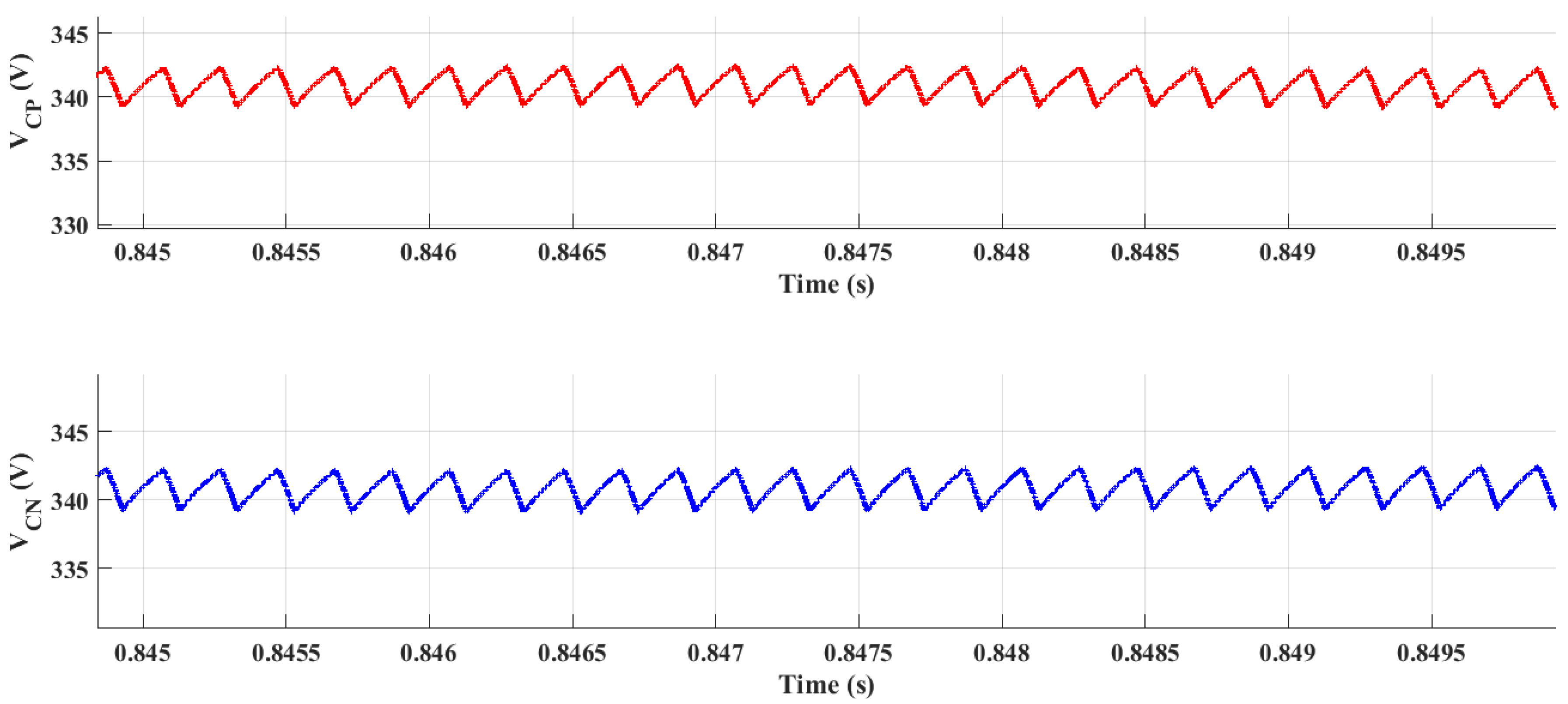
From (21) and (24), the voltage across capacitors V CP and V CN are the same as the pole voltages, having values of 343 V, and the same results are depicted in Figure 9. This ensures the agreement between the mathematically-calculated and simulation results. The voltages across both capacitors are well balanced.
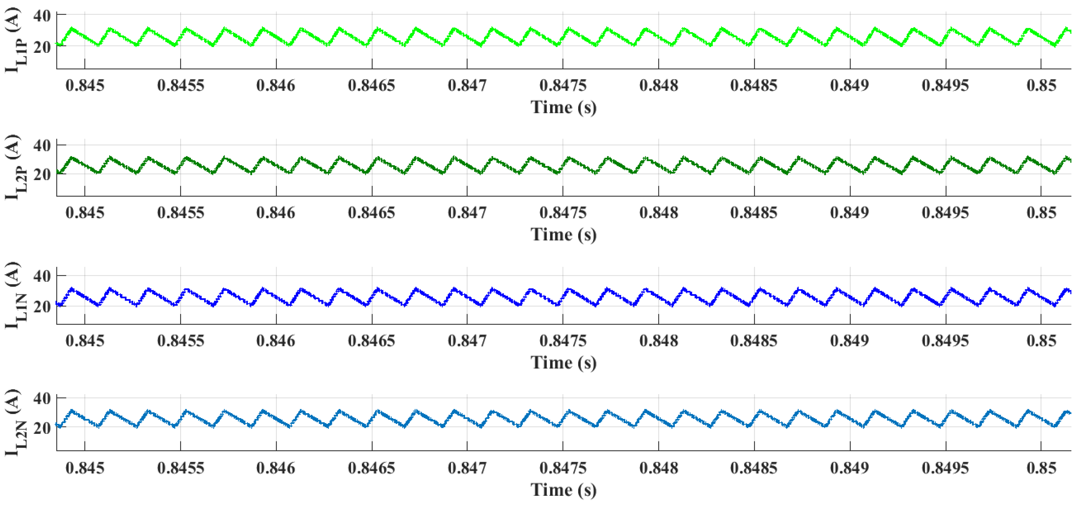
The waveforms for the inductor currents I L 1 P , I L 2 P , I L 1 N , and I L 2 N are shown in Figure 10.
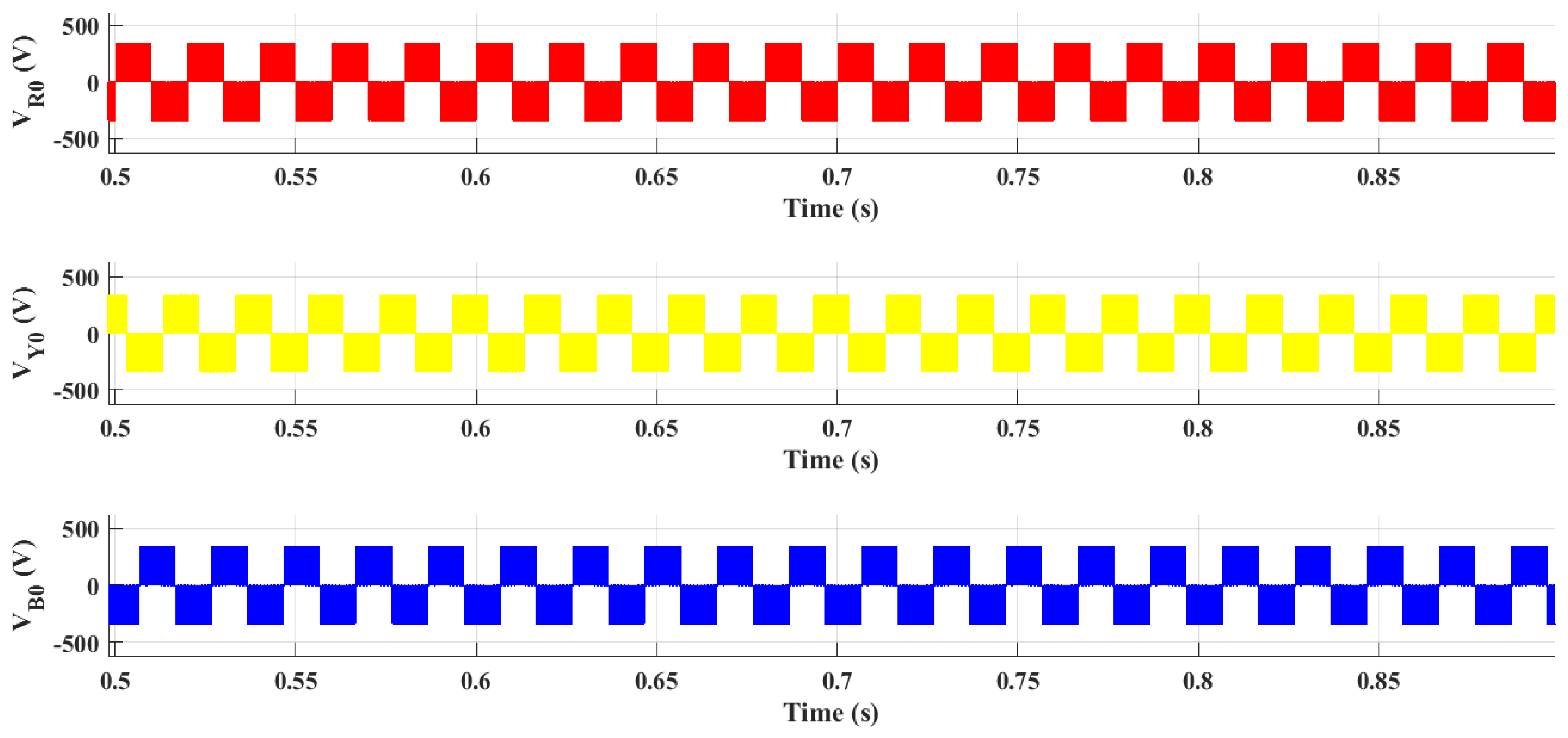
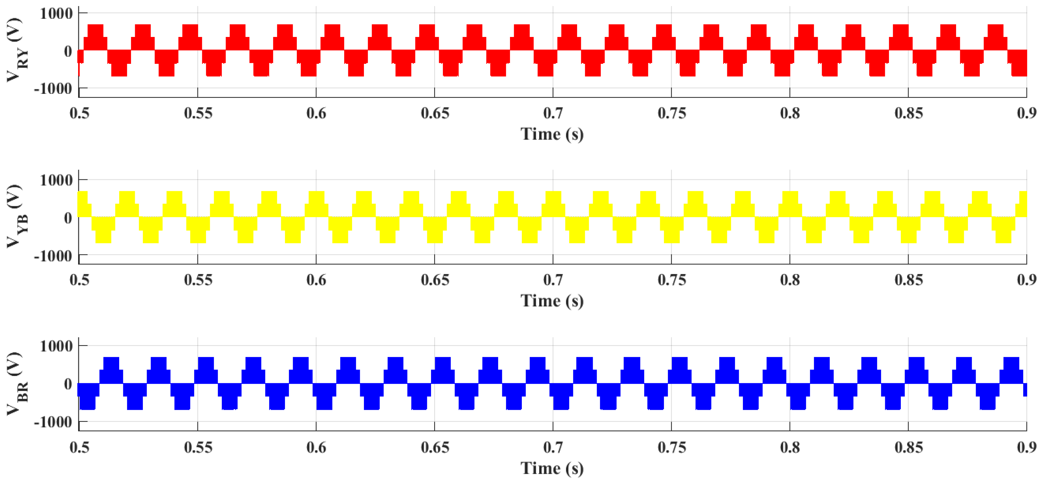
Line voltage and phase voltage are shown in Figure 11 and Figure 12, respectively. Line voltages are the difference of the pole voltages having a value of 687 V as depicted in the simulation results. Line voltages and phase voltages (the voltages between the phase and neutral points of star-connected load) are interrelated as:
{ V R Y = V R 0 V Y 0 V Y B = V Y 0 V B 0 V B R = V B 0 V R 0
{ V R N = V R Y V Y B 3 V B N = V B R V R Y 3 V Y N = V Y B V B R 3
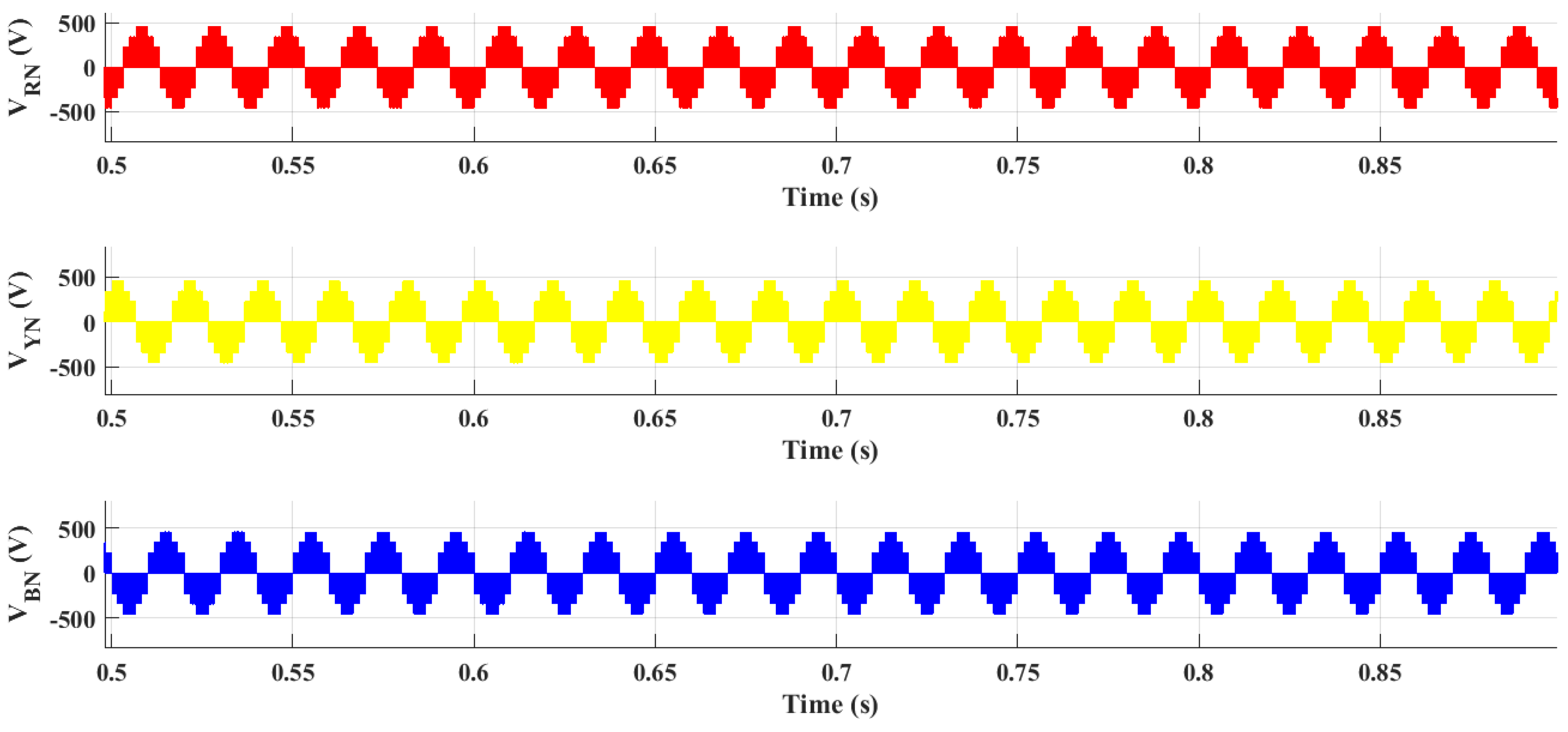
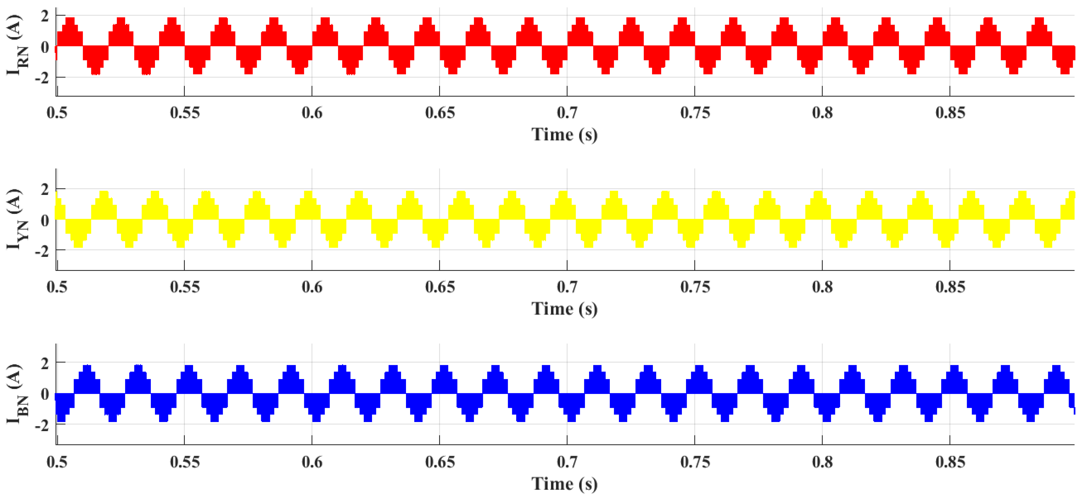
A star-connected resistive load having a resistance of 250 Ω per phase is deployed at the output of the inverter. The waveforms of phase currents are shown in Figure 13, that are in-phase with the voltage, thus improving the power quality.
All the simulation results are identical to the theoretical analysis performed for the inverter.

6. Comparison with Previous Topologies

Different parameters, i.e., boosting ability, modulation index, duration of ST duty ratio, and voltage stress across switches, are considered for the comparative analysis purposes to show the effectiveness of the proposed topology. A lot of improvements in the aforementioned parameters offered by the proposed topology are found over the previous topologies.
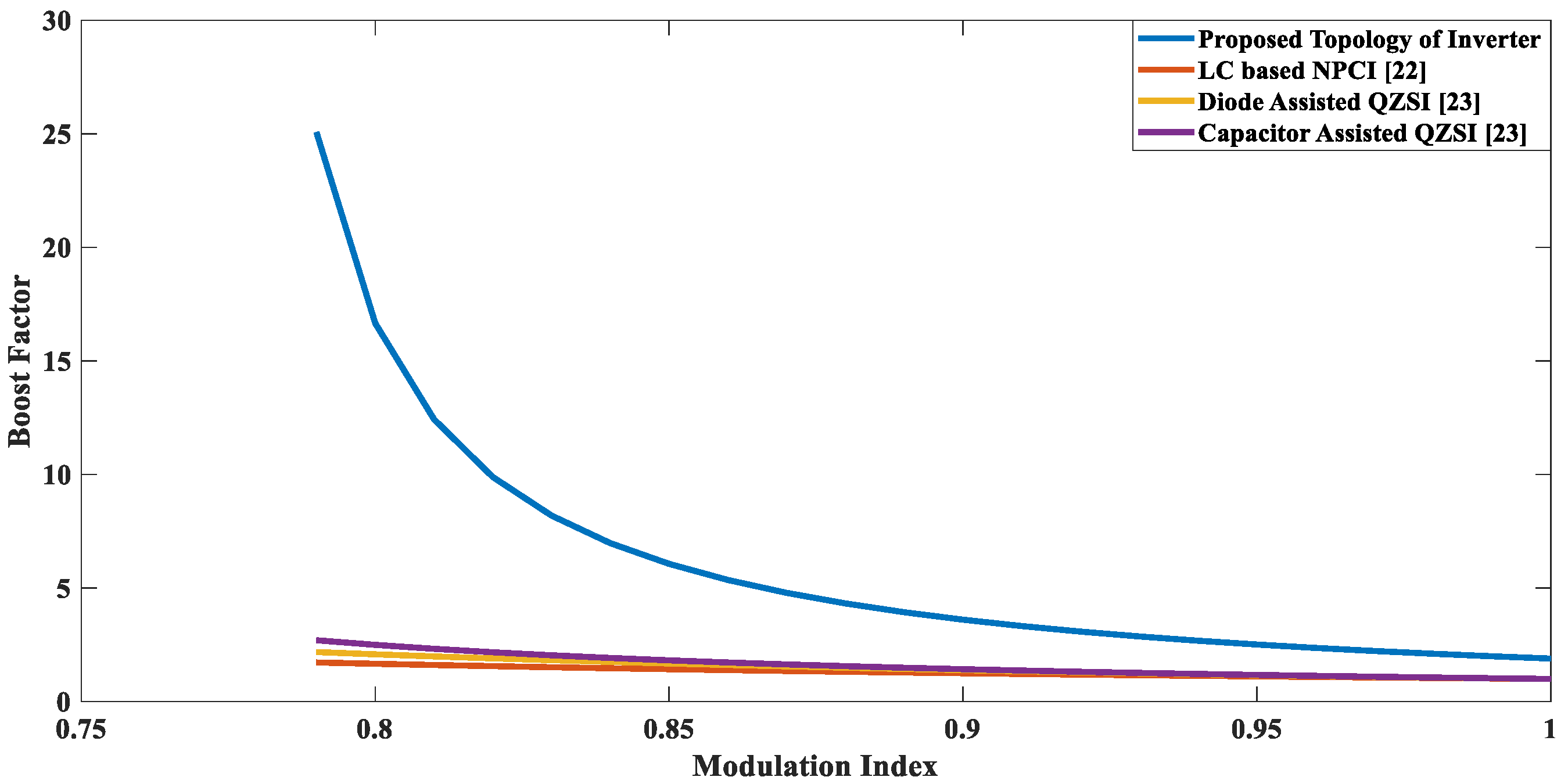
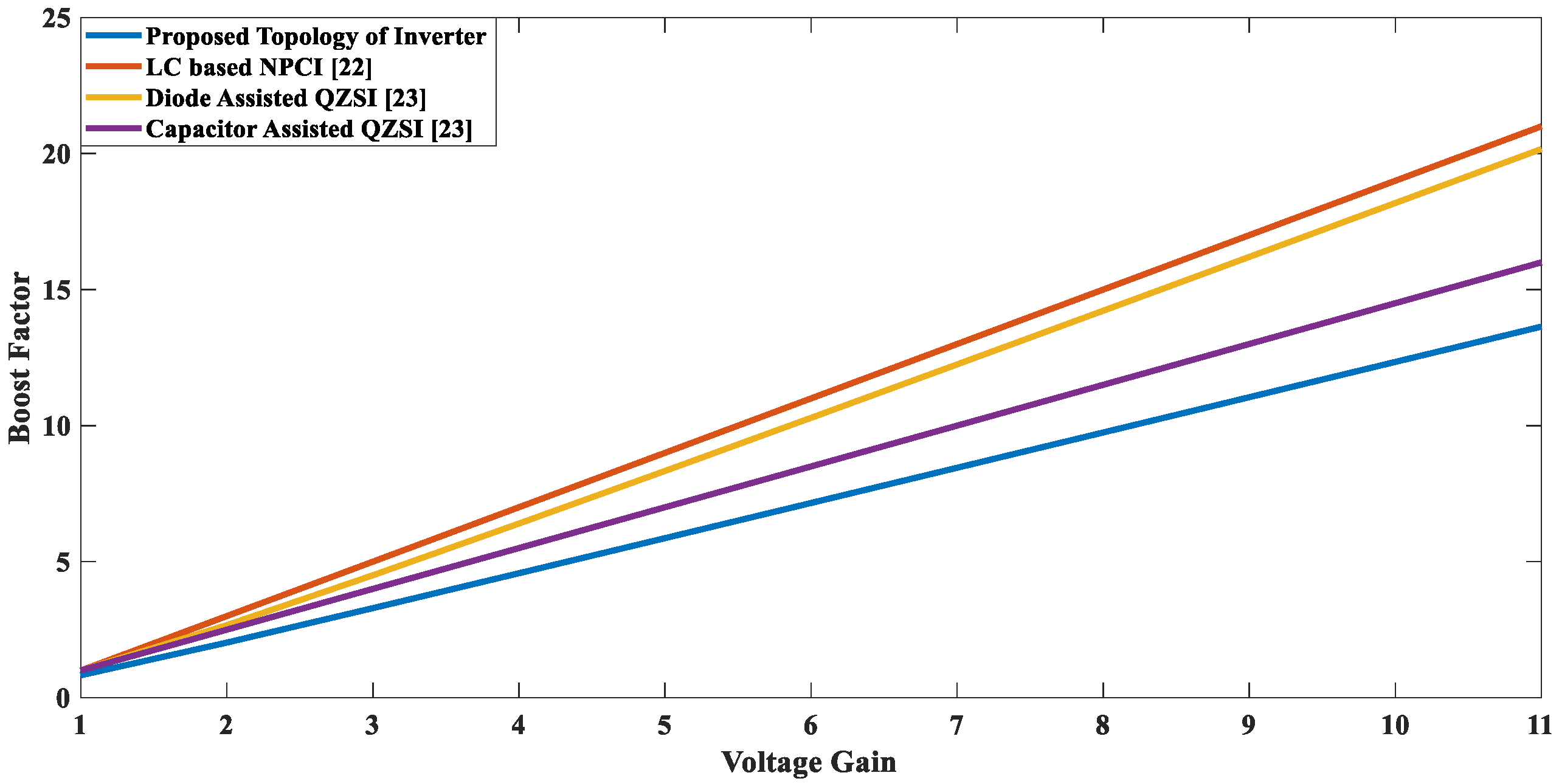
Figure 14 compares the boost factor versus modulation index for the proposed and the previous topologies, which indicates that the boost factor of the proposed topology is much higher than that of the previous topologies for the same values of modulation index. The proposed inverter is capable of exhibiting higher boosting ability even at larger values of modulation index.
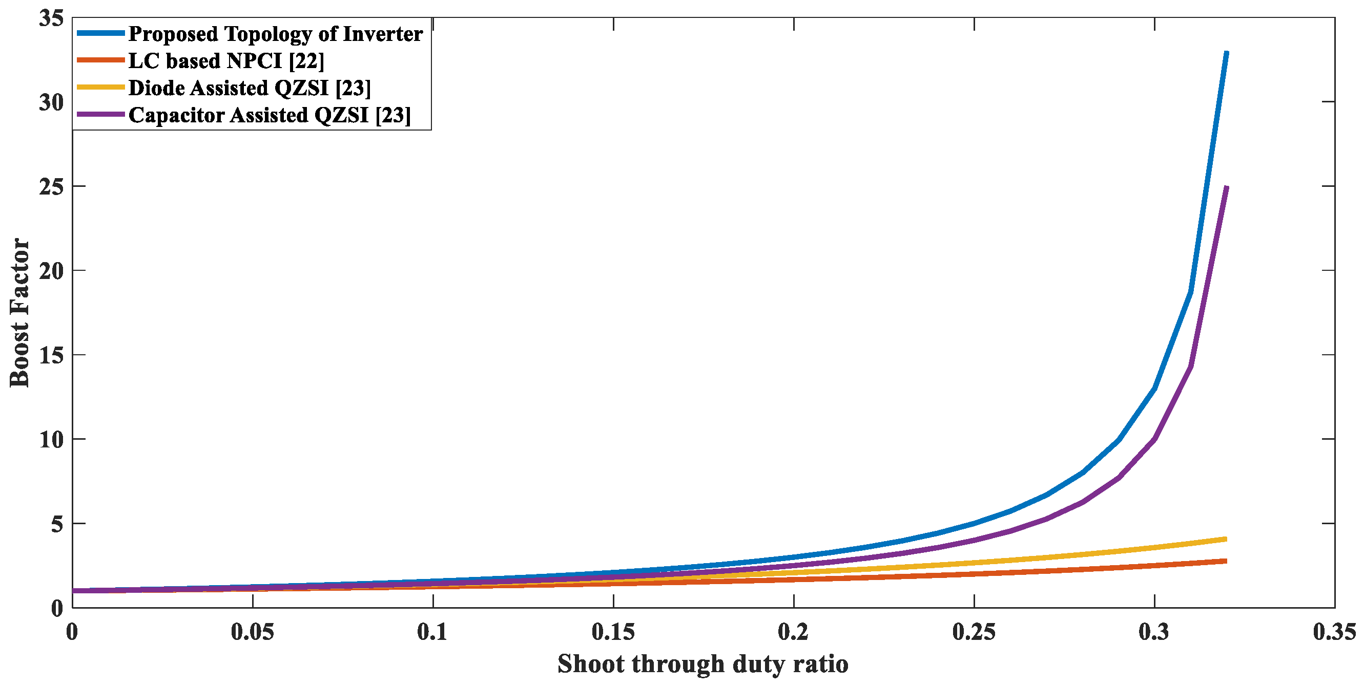
In addition, the proposed topology is most appropriate to achieve a higher boost factor by utilizing a smaller value of D with a wide range of modulation index. 
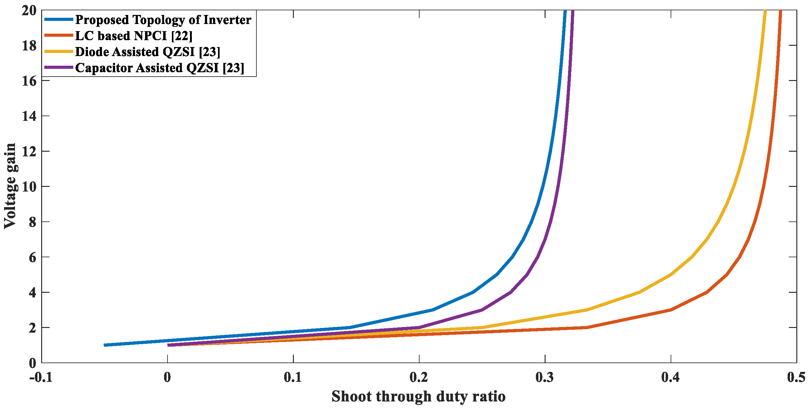
Figure 15 shows a relationship of boost factor versus the ST duty ratio for the proposed and the previous topologies. It can be seen that the proposed topology offers better results, even with smaller values of the ST duty ratio. Thus, this topology can be deployed in applications where higher boost is required with a smaller ST duty ratio.
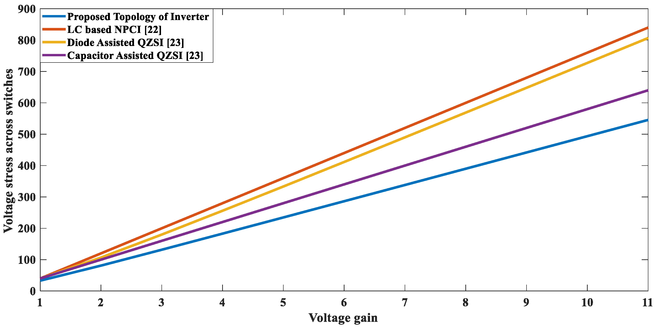
The proposed topology also shows a remarkable boosting ability with lower voltage stress across the switches. Figure 16 shows a graph between stress across switches and voltage gain, for the proposed topology and the previous topologies, indicating that the proposed topology offers much better results. It enables the availability of higher boost without increasing the stress much. Lowering in switching voltage stresses leads to the reduction of the rating of switches and the size of inverter.
Figure 17 depicts the voltage gain versus the ST duty ratio, which indicates the superiority of proposed topology over the previous topologies in terms of higher voltage gain with lower values of shoot-through duty ratio.
Figure 18 demonstrates the relationship between boost factor and voltage gain and exhibits that the proposed topology offers the higher voltage gain against the appropriate value of boost factor due to the availability of higher modulation index, whereas, with previous topologies, significantly lower voltage gain can be achieved from the given boost factor. It can be seen from the graph that with the proposed topology, the values of voltage gain are near the corresponding values of the boost factor.
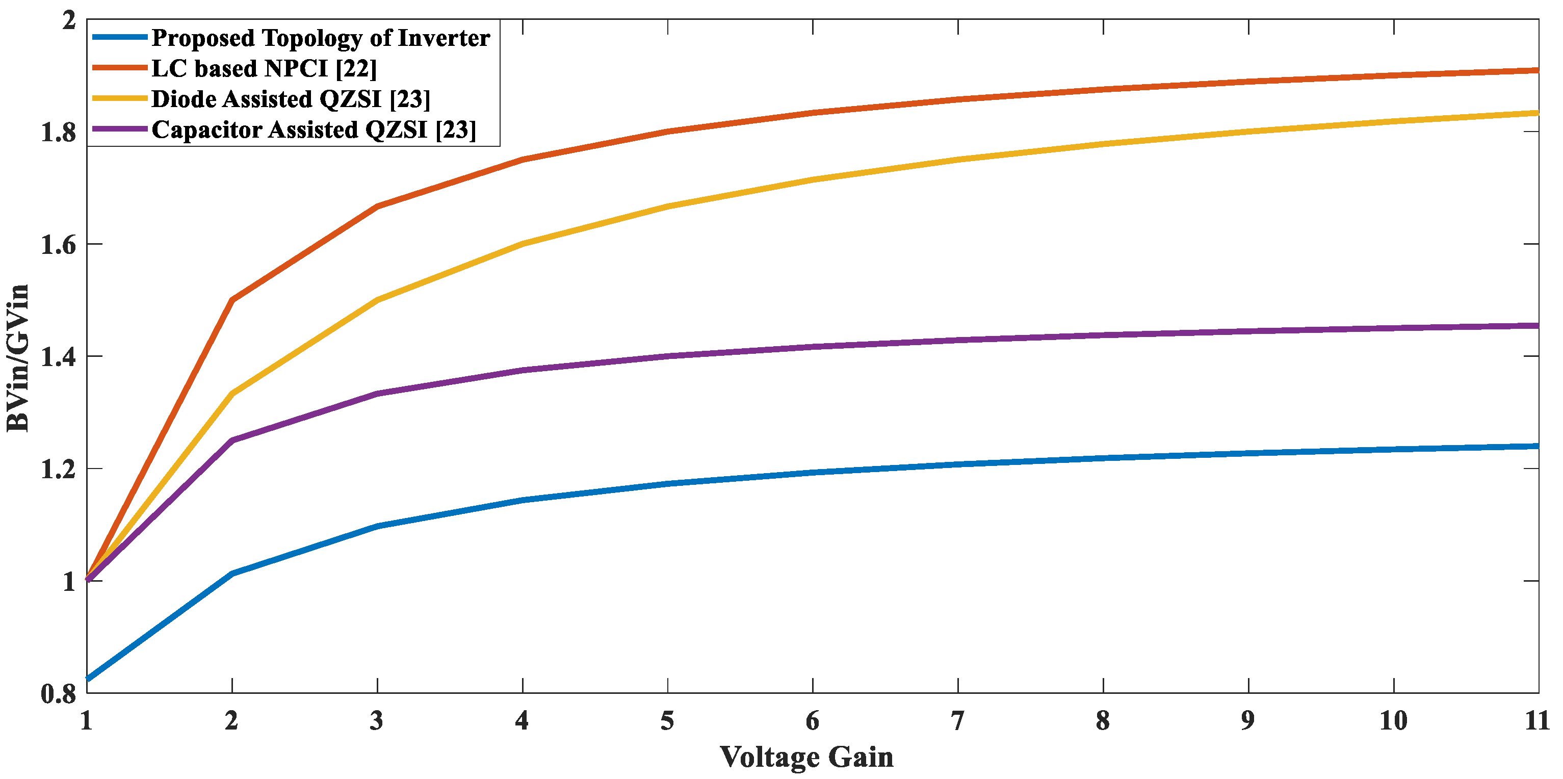
In Figure 19, a graph is plotted between BVin/GVin versus the voltage gain, showing clearly that the proposed topology offers better results as compared to previous topologies.
The simulation results ensure the superiority of the proposed inverter topology over the existing ones. These simulation results can easily be translated into mathematical relations.
In a nutshell, mathematically speaking, a detailed comparison of all such parameters is shown in Table 5. On taking any combination of the input parameters, the output parameters (column 1 of Table 5) are found improved for the proposed topology over the existing ones, just like the simulation results.
Efficiency analysis of the proposed inverter topology is also performed and compared with the previous topologies. Table 6 shows the values of components/parameters used for the analysis. For comparison purposes, they are assumed to be the same for all the topologies. For the simplicity of efficiency analysis, the power losses across the inductors, capacitors, diodes, and active switches (where applicable) due to parasitic resistance of inductors and capacitors, the forward voltage drop of diodes, and on-resistance of active switches are considered.
Table 7 shows the equivalent circuits during the NST and ST state of the topologies to be compared. Correspondingly, the power losses that occur across the inductors, capacitors, diodes, and active switches (where applicable) during NST and ST were calculated by utilizing the technique given in [33,34], Expressions of U series (U1, U2, U3, and U4), V series (V1, V2, V3, and V4), W series (W1, W2, W3 and W4), and Z series (Z3, Z4) in Table 7 show the power losses across the inductors, capacitors, diodes, and active switches during NST and ST state, respectively.
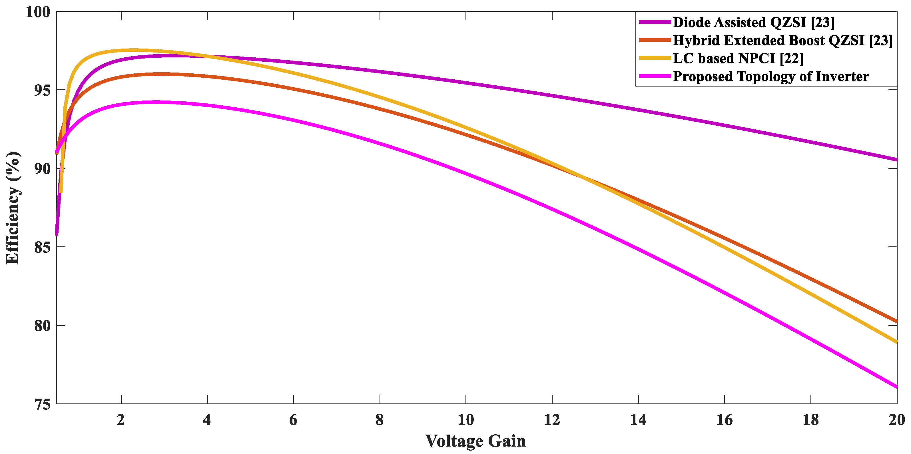
The efficiency of each topology against the overall voltage gain is computed. As can be observed from Figure 20, efficiency curves of all considered topologies are comparable with one another with a minor difference. The proposed topology offers more than 90% efficiency with a voltage gain of up to 10. With this level of efficiency, it offers several advantages in the form of higher boosting ability, lesser voltage stresses across the switches, lower shoot-through duty ratio, availability of higher modulation index, and improved quality of output waveform by reducing the THD. The reduction in voltage stresses across the switches ensures the utilization of lower rating components/devices even for a higher voltage gain, whereas in the previous topologies, the stresses across the devices drastically increase as the voltage gain increases, as depicted in Figure 16. This situation demands an enormous increase in the rating of components/devices used in previous topologies of the inverter, which leads to a tremendous increase in the cost of components/devices and the size of the inverter, which makes it bulky.
To extend our discussion further, by utilizing Table 5 and Figure 16, Figure 17, Figure 18, Figure 19 and Figure 20, a detailed comparison of the proposed inverter topology with the previous inverter topologies in terms of overall efficiency, stresses across switches, rating of components/devices, cost, and size is performed and depicted in 
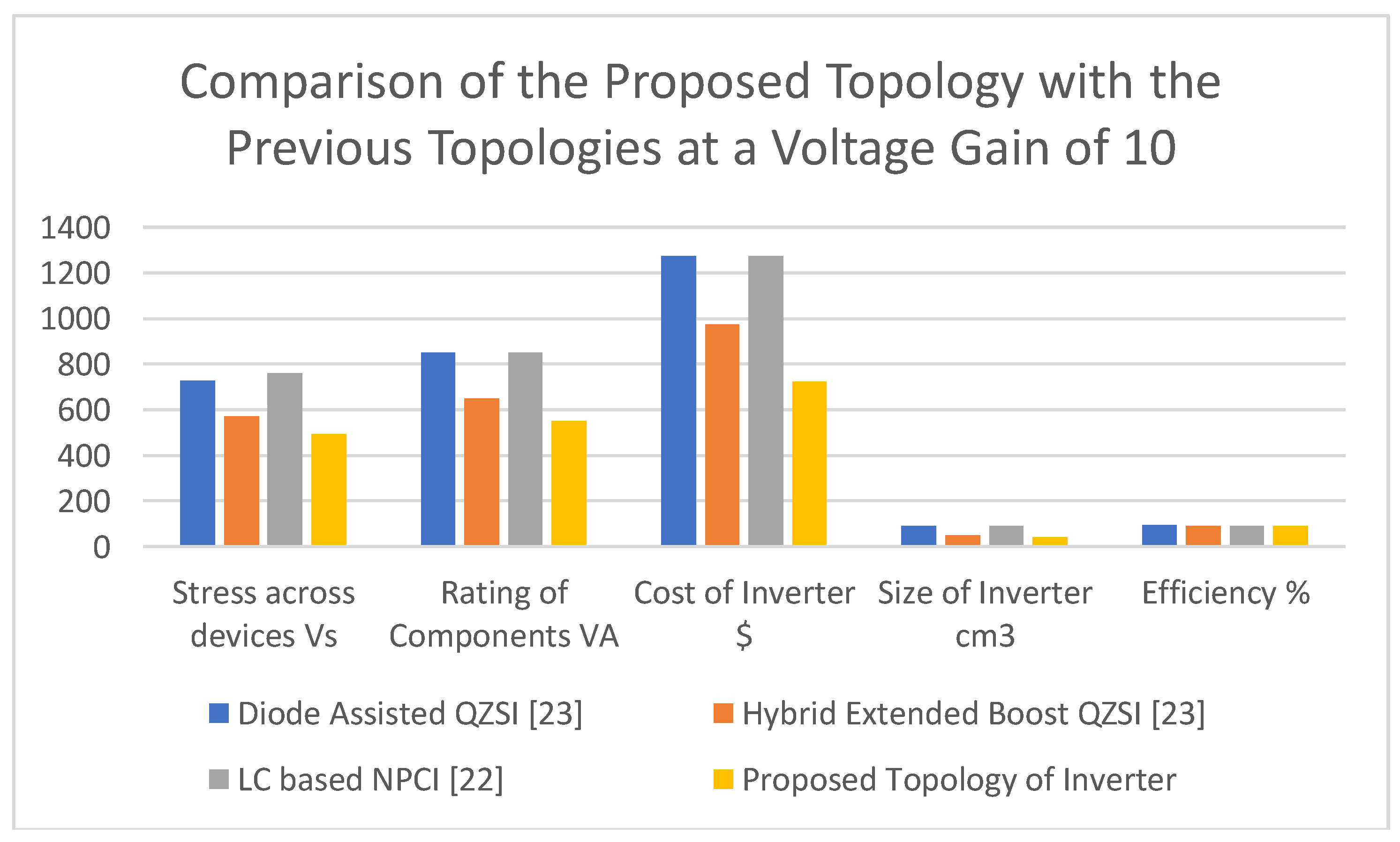
Figure 21, for a voltage gain of 10 (this voltage is taken as a sample, although the analysis for other values is also true).
It is clear from the comparison that the proposed topology is more feasible for the practical applications as compared to the previous topologies, especially when more voltage gain and boosting ability are required and when cost, size, and lower rating of components are the main concerns. Since the proposed topology belongs to the ZSI family, it finds its applications where all other ZSI are applicable, such as in variable speed drive systems, grid-connected photovoltaic systems, distributed generation systems, hybrid electric vehicles, laminators, conveyor belts, and so on [35,36,37].

7. Conclusions

This research work focused on the development of the three-level high voltage gain NPCI topology to boost up the DC voltage at the desired level and offers the three-level AC output in a single stage. It also detained all the merits of previous topologies of three-level NPCZSI/QZSI, such as continuity in input current and voltage balance across the capacitors. The results validated that the proposed topology ensures the remarkable boosting ability by utilizing the smaller duration of ST state and higher range of modulation index, which enables it to keep the lower stresses across the devices even at higher values of voltage gain; that is the most desirable feature for low voltage applications. The proposed topology has a slightly lower efficiency compared to other topologies; however, it reduces cost and size by utilizing the low rating components at higher voltage gain operations. This unique feature makes it more feasible for practical applications as compared to other topologies that oblige the higher rating components for their operation; this drawback associated with previous topologies not only affects the cost of the inverter but also makes the size of inverter bulky and voluminous.

Author Contributions

Conceptualization, G.A. and I.K.; methodology, M.A.A. and R.M.; software, A.B.A.; validation, U.F. and S.S.K.; formal analysis, S.S.K.; investigation, M.A.A.; resources, G.A.; data curation, M.A.A.; writing—original draft preparation, G.A.; writing—review and editing, I.K.; visualization, U.F. and R.M.; supervision, A.B.A.; project administration, G.A.; funding acquisition, I.K. All authors have read and agreed to the published version of the manuscript.

Funding

This research received no external funding.

Conflicts of Interest

The authors declare no conflict of interest.

References

  1. Tang, Y.; Xie, S.; Zhang, C. An improved Z-source inverter. IEEE Trans. Power Electron. 2010, 26, 3865–3868. [Google Scholar] [CrossRef]
  2. Ding, X.; Qian, Z.; Yang, S.; Cui, B.; Peng, F. A high-performance Z-source inverter operating with small inductor at wide-range load. In Proceedings of the APEC 07-Twenty-Second Annual IEEE Applied Power Electronics Conference and Exposition, Anaheim, CA, USA, 25 Feburary–1 March 2007; pp. 615–620. [Google Scholar]
  3. Tang, Y.; Xie, S.; Zhang, C.; Xu, Z. Improved Z-source inverter with reduced Z-source capacitor voltage stress and soft-start capability. IEEE Trans. Power Electron. 2009, 24, 409–415. [Google Scholar] [CrossRef]
  4. Vinnikov, D.; Roasto, I.; Jalakas, T. An improved high-power DC/DC Converter for distributed power generation. In Proceedings of the 2009 10th International Conference on Electrical Power Quality and Utilisation, Lodz, Poland, 15–17 September 2009; pp. 1–6. [Google Scholar]
  5. Anderson, J.; Peng, F.Z. A class of quasi-Z-source inverters. In Proceedings of the 2008 IEEE Industry Applications Society Annual Meeting, Edmonton, AB, Canada, 5–9 October 2008; pp. 1–7. [Google Scholar]
  6. Anderson, J.; Peng, F.Z. Four quasi-Z-source inverters. In Proceedings of the 2008 IEEE Power Electronics Specialists Conference, Rhodes, Greece, 15–19 June 2008; pp. 2743–2749. [Google Scholar]
  7. Peng, F.Z.; Yuan, X.; Fang, X.; Qian, Z. Z-source inverter for adjustable speed drives. IEEE Power Electron. Lett. 2003, 1, 33–35. [Google Scholar] [CrossRef]
  8. Li, Y.; Anderson, J.; Peng, F.Z.; Liu, D. Quasi-Z-source inverter for photovoltaic power generation systems. In Proceedings of the 2009 Twenty-Fourth Annual IEEE Applied Power Electronics Conference and Exposition, Washington, DC, USA, 15–19 February 2009; pp. 918–924. [Google Scholar]
  9. Ismeil, M.A.; Kouzou, A.; Kennel, R.; Abu-Rub, H.; Orabi, M. A new switched-inductor quasi-Z-source inverter topology. In Proceedings of the 2012 15th International Power Electronics and Motion Control Conference (EPE/PEMC), Novi Sad, Serbia, 4–6 September 2012; pp. DS3d.2-1–DS3d.2-6. [Google Scholar]
  10. Mosa, M.; Abu-Rub, H.; Rodríguez, J. High performance predictive control applied to three phase grid connected Quasi-Z-Source Inverter. In Proceedings of the IECON 2013-39th Annual Conference of the IEEE Industrial Electronics Society, Vienna, Austria, 10–13 November 2013; pp. 5812–5817. [Google Scholar]
  11. Loh, P.C.; Gao, F.; Blaabjerg, F.; Goh, A.L. Buck-boost impedance networks. In Proceedings of the 2007 European Conference on Power Electronics and Applications, Aalborg, Denmark, 2–5 September 2007; pp. 1–10. [Google Scholar]
  12. Loh, P.C.; Gao, F.; Blaabjerg, F. Embedded EZ-source inverters. IEEE Trans. Ind. Appl. 2009, 46, 256–267. [Google Scholar]
  13. Loh, P.C.; Gao, F.; Blaabjerg, F.; Feng, S.Y.C.; Soon, K.N.J. Pulsewidth-Modulated $ Z $-Source Neutral-Point-Clamped Inverter. IEEE Trans. Ind. Appl. 2007, 43, 1295–1308. [Google Scholar] [CrossRef]
  14. Loh, P.C.; Blaabjerg, F.; Wong, C.P. Comparative evaluation of pulse-width modulation strategies for Z-source neutral-point-clamped inverter. In Proceedings of the 2006 37th IEEE Power Electronics Specialists Conference, Jeju, Korea, 18–22 June 2006; pp. 1–7. [Google Scholar]
  15. Loh, P.C.; Lim, S.W.; Gao, F.; Blaabjerg, F. Three-level Z-source inverters using a single LC impedance network. IEEE Trans. Power Electron. 2007, 22, 706–711. [Google Scholar] [CrossRef]
  16. Loh, P.C.; Gao, F.; Blaabjerg, F.; Lim, S.W. Operational analysis and modulation control of three-level Z-source inverters with enhanced output waveform quality. IEEE Trans. Power Electron. 2009, 24, 1767–1775. [Google Scholar] [CrossRef]
  17. Maheshwari, R.; Munk-Nielsen, S.; Busquets-Monge, S. Design of neutral-point voltage controller of a three-level NPC inverter with small DC-link capacitors. IEEE Trans. Ind. Electron. 2012, 60, 1861–1871. [Google Scholar] [CrossRef]
  18. Mo, W.; Loh, P.C.; Blaabjerg, F.; Wang, P. Trans-Z-source and Γ-Z-source neutral-point-clamped inverters. IET Power Electron. 2014, 8, 371–377. [Google Scholar] [CrossRef]
  19. Wang, X.; Liu, H.; Li, Y. A novel coupled inductor Z-source three-level inverter. IEICE Electron. Express 2017, 14. [Google Scholar] [CrossRef]
  20. Battiston, A.; Miliani, E.-H.; Pierfederici, S.; Meibody-Tabar, F. A novel quasi-Z-source inverter topology with special coupled inductors for input current ripples cancellation. IEEE Trans. Power Electron. 2015, 31, 2409–2416. [Google Scholar] [CrossRef] [Green Version]
  21. Yahya, A.; Waqar, T.; Husain, N.; Ali, S.M.U. Hybrid Multilevel Topology Based High Power Quality Inverter. In Proceedings of the APEC’98 Thirteenth Annual Applied Power Electronics Conference and Exposition, Anaheim, CA, USA, 15–19 February 1998. [Google Scholar]
  22. Sahoo, M.; Keerthipati, S. A three-level LC-switching-based voltage boost NPC inverter. IEEE Trans. Ind. Electron. 2016, 64, 2876–2883. [Google Scholar] [CrossRef]
  23. Gajanayake, C.J.; Luo, F.L.; Gooi, H.B.; So, P.L.; Siow, L.K. Extended-boost $ Z $-source inverters. IEEE Trans. Power Electron. 2010, 25, 2642–2652. [Google Scholar] [CrossRef]
  24. Peng, F.Z. Z-Source Inverter. IEEE Trans. Ind. Appl. 2003, 39. [Google Scholar] [CrossRef]
  25. Nabae, A.; Takahashi, I.; Akagi, H. A new neutral-point-clamped PWM inverter. IEEE Trans. Ind. Appl. 1981, 5, 518–523. [Google Scholar] [CrossRef]
  26. McGrath, B.P.; Holmes, D.G. Multicarrier PWM strategies for multilevel inverters. IEEE Trans. Ind. Electron. 2002, 49, 858–867. [Google Scholar] [CrossRef]
  27. Rathore, S.; Kirar, M.K.; Bhardwaj, S.K. Simulation of cascaded H-bridge multilevel inverter using PD, POD, APOD techniques. Electr. Comput. Eng. Int. J. ECIJ 2015, 4, 27–41. [Google Scholar] [CrossRef]
  28. Haskar Reddy, V.N.; Babu, C.S.; Suresh, K. Advanced Modulating Techniques for Diode Clamped Multilevel Inverter Fed Induction Motor. ARPN J. Eng. Appl. Sci. 2011, 6, 90–99. [Google Scholar]
  29. Colak, I.; Kabalci, E.; Bayindir, R. Review of multilevel voltage source inverter topologies and control schemes. Energy Convers. Manag. 2011, 52, 1114–1128. [Google Scholar] [CrossRef]
  30. McGrath, B.P.; Holmes, D.G. A comparison of multicarrier PWM strategies for cascaded and neutral point clamped multilevel inverters. In Proceedings of the 2000 IEEE 31st Annual Power Electronics Specialists Conference. Conference Proceedings (Cat. No. 00CH37018), Galway, Ireland, 23 June 2000; Volume 2, pp. 674–679. [Google Scholar]
  31. Peng, F.Z.; Shen, M.; Qian, Z. Maximum boost control of the Z-source inverter. IEEE Trans. Power Electron. 2005, 20, 833–838. [Google Scholar] [CrossRef]
  32. Shen, M.; Wang, J.; Joseph, A.; Peng, F.Z.; Tolbert, L.M.; Adams, D.J. Constant boost control of the Z-source inverter to minimize current ripple and voltage stress. IEEE Trans. Ind. Appl. 2006, 42, 770–778. [Google Scholar] [CrossRef]
  33. Pan, L. LZ-source inverter. IEEE Trans. Power Electron. 2014, 29, 6534–6543. [Google Scholar] [CrossRef]
  34. Zhu, X.; Zhang, B.; Qiu, D. Enhanced boost quasi-Z-source inverters with active switched-inductor boost network. IET Power Electron. 2018, 11, 1774–1787. [Google Scholar] [CrossRef]
  35. Rodriguez, J.; Lai, J.-S.; Peng, F.Z. Multilevel inverters: A survey of topologies, controls, and applications. IEEE Trans. Ind. Electron. 2002, 49, 724–738. [Google Scholar] [CrossRef] [Green Version]
  36. Peng, F.Z.; Joseph, A.; Wang, J.; Shen, M.; Chen, L.; Pan, Z.; Ortiz-Rivera, E.; Huang, Y. Z-source inverter for motor drives. IEEE Trans. Power Electron. 2005, 20, 857–863. [Google Scholar] [CrossRef]
  37. Khlebnikov, A.S.; Kharitonov, S.A. Application of the Z-source converter for aircraft power generation systems. In Proceedings of the 2008 9th International Workshop and Tutorials on Electron Devices and Materials, Novosibirsk, Russia, 1–5 July 2008; pp. 211–215. [Google Scholar]
Figure 1. The proposed topology of the inverter.
Energies 13 01261 g001
Figure 2. Equivalent circuit for the active state.
Energies 13 01261 g002
Figure 3. Equivalent circuit for the zero-state.
Energies 13 01261 g003
Figure 4. Equivalent circuit for the ST state.
Energies 13 01261 g004
Figure 5. Gating signals for the main inverter circuit.
Energies 13 01261 g005
Figure 6. GS to AS01 and AS02.
Energies 13 01261 g006
Figure 7. MCBCM with PODSPWM.
Energies 13 01261 g007
Figure 8. Pole voltage V RO , V YO and V BO .
Energies 13 01261 g008
Figure 9. Voltage across capacitors V CP and V CN .
Energies 13 01261 g009
Figure 10. Inductor currents I L 1 P , I L 2 P , I L 1 N and I L 2 N .
Energies 13 01261 g010
Figure 11. Line voltage V RY , V YB , and V BR .
Energies 13 01261 g011
Figure 12. Phase voltage V RN , V YN , and V BN .
Energies 13 01261 g012
Figure 13. Load currents I RN , I YN , and I BN .
Energies 13 01261 g013
Figure 14. Boost factor versus modulation index.
Energies 13 01261 g014
Figure 15. Boost factor versus ST duty ratio.
Energies 13 01261 g015
Figure 16. Voltage stress versus gain.
Energies 13 01261 g016
Figure 17. ST duty ratio versus gain.
Energies 13 01261 g017
Figure 18. Gain versus boost factor.
Energies 13 01261 g018
Figure 19. BVin/GVin versus gain.
Energies 13 01261 g019
Figure 20. Efficiency versus voltage gain.
Energies 13 01261 g020
Figure 21. A detailed comparison of the proposed topology with the previous topologies.
Energies 13 01261 g021
Table 1. Different approaches for ST state.
Sr. No.ON SwitchesOFF Switches
1 S R 1 , S R 2 , S R 3 , S R 4 , A S 01 , A S 02 S Y 1 , S Y 2 , S Y 3 , S Y 4 , S B 1 , S B 2 , S B 3 , S B 4
2 S Y 1 , S Y 2 , S Y 3 , S Y 4 , A S 01 , A S 02 S R 1 , S R 2 , S R 3 , S R 4 , S B 1 , S B 2 , S B 3 , S B 4
3 S B 1 , S B 2 , S B 3 , S B 4 , A S 01 , A S 02 S R 1 , S R 2 , S R 3 , S R 4 , S Y 1 , S Y 2 , S Y 3 , S Y 4
4 S R 1 , S R 2 , S R 3 , S R 4 , S Y 1 , S Y 2 , S Y 3 , S Y 4 , A S 01 , A S 02 S B 1 , S B 2 , S B 3 , S B 4
5 S R 1 , S R 2 , S R 3 , S R 4 , S B 1 , S B 2 , S B 3 , S B 4 , A S 01 , A S 02 S Y 1 , S Y 2 , S Y 3 , S Y 4
6 S Y 1 , S Y 2 , S Y 3 , S Y 4 , S B 1 , S B 2 , S B 3 , S B 4 , A S 01 , A S 02 S R 1 , S R 2 , S R 3 , S R 4
7 S R 1 , S R 2 , S R 3 , S R 4 , S Y 1 , S Y 2 , S Y 3 , S Y 4 , S B 1 , S B 2 , S B 3 , S B 4 , A S 01 , A S 02 Nil
Table 2. Parameters specifications of the proposed inverter topology.
Parameters/ComponentValue
Applied DC Voltage40 V
Capacitor1000 µF
Inductor2 mH
Load250 Ω
Frequency of Reference Signal(s)50 Hz
Frequency of Carrier Signal(s)5000 Hz
Modulation Index, M0.825
Shoot Through Duty Ratio, D0.2855291
Boost Factor8.96
Overall Voltage Gain, G7.392
Table 3. Device parameters in the proposed inverter topology.
DeviceParameterValue
DiodeInternal Resistance0.001 Ω
Forward Voltage Drop0.7 V
Snubber Resistance500 Ω
Snubber Capacitanceinf
Active SwitchInternal Resistance0.001 Ω
Snubber Resistance1 × 105
Snubber Capacitanceinf
IGBTInternal Resistance0.01 Ω
Snubber Resistance1 × 105
Snubber Capacitance1000 F
Table 4. Boosting ability against different values of M and D.
ST Duty Ratio (D)Modulation Index (M)Boost Factor (B)
0.111.02771.6567
0.131.00461.8525
0.150.98152.0909
0.170.95842.3878
0.190.93532.7674
0.210.91223.2703
0.230.88913.9677
0.250.8665.0
0.270.84296.6842
0.28550.8258.96
0.290.81989.9231
0.310.796718.7143
0.320.785233
0.330.7736133
Table 5. Comparison with previous topologies.
ParameterProposed Inverter TopologyLC-based NPCI [22]Diode Assisted [23] QZSICapacitor Assisted QZSI [23]
Boost Factor B = 1 + D 1 3 D
B = 4 3 M 3 3 M 4
B = 2 3 G 4 3 3 G + 27 G 2 8 3 G + 16
B = 1 1 2 D
B = 1 2 M 1
B = 2 G 1
B = 1 1 + 2 D 2 3 D
B = 1 2 M 2 M
B = 2 G 2 1 + G
B = 1 1 3 D
B = 1 3 M 2
B = 3 G 1 2
Voltage Gain G = M ( 4 3 M ) 3 3 M 4 G = M 2 M 1 G = 1 2 M 1 G = M 3 M 2
Modulation Index M = 4 3 3 G + 27 G 2 8 3 G + 16 2 3 M = G 2 G 1 M = 1 + G 2 G M = 2 G 3 G 1
Shoot- Through Duty Ratio D = 3 3 G 27 G 2 8 3 G + 16 4 D = G 1 2 G 1 D = G 1 2 G D = G 1 3 G 1
Stress Across Switches V s = ( 4 3 M ) V i n 3 3 M 4
V s = ( 2 3 G 4 3 3 G + 27 G 2 8 3 G + 16 ) V i n
V s = V i n 2 M 1
V s = ( 2 G 1 ) V i n
V s = ( 1 2 M 2 M ) V i n
V s = ( 2 G 2 1 + G ) V i n
V s = ( 1 3 M 2 ) V i n
V s = ( 3 G 1 2 ) V i n
Table 6. Detail of components/parameters used in the efficiency analysis.
Component/ParameterSymbolValue
ESR of CapacitorRC0.08 Ω
DCR of InductorRL0.07 Ω
On-Resistance of Active SwitchRS0.001 Ω
Load ResistanceRl250 Ω
Applied DC VoltageVin40 V
Voltage Drop Across DiodeVF0.7 V
Table 7. Efficiency analysis of various topologies.
TopologyNST StateST StateEfficiency
Diode Assisted QZSI [23] Energies 13 01261 i001
P 11 = ( 1 D ) 2 ( 2 I L 1 2 + I L 3 2 ) R L + ( 1 D ) ( 2 I L 1 + I L 3 I l o a d ) V F + ( 1 D ) 2 [ 2 ( I L 1 I l o a d ) 2 + ( I L 3 I l o a d ) 2 ] R C
Energies 13 01261 i002
P 12 = D 2 ( 2 I L 1 2 + I L 3 2 ) R L + D 2 6 I L 1 2 R C + D I L 3 V F
η 3 = V o u t I l o a d P 33 + P 34 + V o u t I l o a d × 100 %
η 1 = 1 U 1 + V 1 + W 1 + 1 × 100 %
U 1 = R L [ 2 ( 1 D ) 5 + ( 1 D ) 3 + 2 D 2 ( 1 D ) 3 + D 2 ( 1 D ) ] R l ( 1 2 D ) 2
V 1 = R C [ 2 ( 1 D ) 5 4 ( 1 D ) 4 ( 1 2 D ) + ( 1 D ) 3 { 3 ( 1 2 D ) 2 + 6 D 2 2 ( 1 2 D ) + 1 } ] R l ( 1 2 D ) 2
W 1 = V F V i n [ 2 ( 1 D ) 3 + ( 1 D ) 2 + D ( 1 D ) ]
Hybrid Extended Boost QZSI [23] Energies 13 01261 i003
P 22 = ( 1 D ) 2 ( 3 I L 1 2 + I L 4 2 ) R L + 3 I L 1 V F + ( 1 D ) 2 [ ( I L 1 I l o a d ) 2 + ( 1 2 D 1 D I L 1 I l o a d ) 2 + 14 D 2 I L 1 2 ( 1 D ) 2 ] R C
Energies 13 01261 i004
P 23 = D 2 ( 3 I L 1 2 + I L 4 2 ) R L + 19 D 2 I L 1 2 R C + D I L 4 V F
η 1 = V o u t I l o a d P 22 + P 23 + V o u t I l o a d × 100 %
η 1 = 1 U 2 + V 2 + W 2 + 1 × 100 %
U 2 = R L ( 1 D ) [ 1 + 3 ( 1 D ) 2 ] [ D 2 + ( 1 D ) 2 ] R l ( 1 3 D ) 2
V 2 = 38 D 2 ( 1 D ) 3 R C ( 1 3 D ) 2 R l
W 2 = V F V i n [ ( 3 2 D ) ( 1 D ) ]
LC-based NPCI [22] Energies 13 01261 i005
P 33 = 2 ( 1 D 2 ) I L 2 R L + 2 ( 1 D ) 2 ( I L I l o a d ) 2 R C + 2 ( 1 D ) I L V F + 2 ( 1 D ) ( I L I l o a d ) V F
Energies 13 01261 i006
P 34 = 2 D 2 I L 2 R L + 2 D 2 I L 2 R S + 2 D 2 I L 2 R C
η 3 = V o u t I l o a d P 33 + P 34 + V o u t I l o a d × 100 %
η 3 = 1 U 3 + V 3 + W 3 + X 3 + 1 × 100 %
U 3 = R L [ 2 ( 1 D ) 5 + 2 D 2 ( 1 D ) 3 ] R l ( 1 2 D ) 2
V 3 = R C [ 2 ( 1 D ) 5 + ( 1 D ) 3 { 2 ( 1 2 D ) 2 + 2 D 2 } 4 ( 1 D ) 4 ( 1 2 D ) ] R l ( 1 2 D ) 2
W 3 = V F V i n [ 4 ( 1 D ) 2 2 ( 1 D ) ( 1 2 D ) ]
X 3 = R S [ 2 D 2 ( 1 D ) 3 ] R l ( 1 2 D ) 2
Proposed Topology of Inverter Energies 13 01261 i007
P 44 = 4 ( 1 D ) 2 I L 2 R L + 2 ( 1 D ) 2 ( I L I l o a d ) 2 R C + 4 ( 1 D ) I L V F + 2 ( 1 D ) ( I L I l o a d ) V F
Energies 13 01261 i008
P 45 = 4 D 2 I L 2 ( R L + 2 R S + 2 R C ) + 4 D I L V F
η 4 = V o u t I l o a d P 44 + P 45 + V o u t I l o a d × 100 %
η 4 = 1 U 4 + V 4 + W 4 + X 4 + 1 × 100 %
U 4 = R L [ 4 ( 1 D ) 5 + 4 D 2 ( 1 D ) 3 ] R l ( 1 3 D ) 2
V 4 = R C [ 2 ( 1 D ) 5 + ( 1 D ) 3 { 2 ( 1 3 D ) 2 + 8 D 2 } 2 ( 1 D ) 2 ( 1 3 D ) ] R l ( 1 3 D ) 2
W 4 = V F [ 6 ( 1 D ) 2 2 ( 1 D ) ( 1 3 D ) + 4 D ( 1 D ) ] V i n ( 1 + D )
X 4 = R S ( 8 D 2 ( 1 D ) 3 ) R l ( 1 3 D ) 2

