Article

LCC-S Based Discrete Fast Terminal Sliding Mode Controller for Efficient Charging through Wireless Power Transfer

1
School of Electrical Engineering, Shandong University, Jinan 250061, China
2
Energy Institute, Qilu University of Technology (Shandong Academy of Sciences), Shandong Provincial Key Laboratory of Biomass Gasification Technology, Jinan 250353, China
3
Department of Electrical Engineering, Jouf University, Al-Jawf, Saudi Arabia
*
Author to whom correspondence should be addressed.
Submission received: 22 December 2019 / Revised: 7 March 2020 / Accepted: 12 March 2020 / Published: 16 March 2020
(This article belongs to the Special Issue Electric Systems for Transportation)

Abstract

:
Compared to the plug-in charging system, Wireless power transfer (WPT) is simpler, reliable, and user-friendly. Resonant inductive coupling based WPT is the technology that promises to replace the plug-in charging system. It is desired that the WPT system should provide regulated current and power with high efficiency. Due to the instability in the connected load, the system output current, power, and efficiency vary. To solve this issue, a buck converter is implemented on the secondary side of the WPT system, which adjusts its internal resistance by altering its duty cycle. To control the duty cycle of the buck converter, a discrete fast terminal sliding mode controller is proposed to regulate the system output current and power with optimal efficiency. The proposed WPT system uses the LCC-S compensation topology to ensure a constant output voltage at the input of the buck converter. The LCC-S topology is analyzed using the two-port network theory, and governing equations are derived to achieve the maximum efficiency point. Based on the analysis, the proposed controller is used to track the maximum efficiency point by tracking an optimal power point. An ultra-capacitor is connected as the system load, and based on its charging characteristics, an optimal charging strategy is devised. The performance of the proposed system is tested under the MATLAB/Simulink platform. Comparison with the conventionally used PID and sliding mode controller under sudden variations in the connected load is presented and discussed. An experimental prototype is built to validate the effectiveness of the proposed controller.

1. Introduction

Wireless power transfer has been desired since the proposition made by Nikola Tesla about 100 years ago [1]. Due to the recent progress in power electronics technology and advancements in WPT techniques, it is realized that implementing a WPT system is now economical and can be used as a commercial product [2]. Compared to the plug-in charging system, WPT is simpler, reliable, and user-friendly [3]. Companies like Qualcomm, Witricity, and Evatran have developed many commercial products that can be charged wirelessly with good efficiency. Due to such developments, WPT can be used in many industrial applications [4] and in our daily life such as wireless charging of smartphones [5], electric vehicles [6,7], and biomedical implants [8,9,10].
According to the operating principles, WPT can be broadly divided into four categories, i.e., capacitive wireless power transfer (CWPT), electromagnetic radiation (EMR), acoustic wireless power transfer (AWPT), and resonant inductive power transfer (RIPT) [11,12]. In CWPT, the power is transferred using capacitor plates instead of coils. CWPT is simpler and can be used for both high voltage and low current, but the efficiency decreases when the air-gap between the transmitter and receiver plate increases [13]. In EMR, the power is transferred using microwaves. Although using this operating principle, WPT can achieve long-distance power transfer, this mode has much lower efficiency and has many health hazards due to high power radiation [14]. In optical wireless power transfer (OWPT), which is considered as a subclass of EMR, the same principles for power transfer are used, but the wavelengths are in the visible spectrum [15,16]. At the transmitting side, lasers are used to convert the electrical signal into the optical signal, and at the receiving side, photovoltaic diodes convert the optical signal back into an electrical signal. The advantage of EMR and OWPT techniques is that both techniques have high capability for power beaming. However, due to the conversion steps, almost 40 to 50% of the energy is lost [15]. In AWPT, the power is transferred by propagating energy in the form of sound or vibration waves. At the transmitting side, the electrical signals are converted into pressure waves by a transducer. The waves propagate through a medium and then are collected by the receiving side transducer, which converts it back into electrical signals. The benefit of AWPT is that it can achieve higher power beam directivity than electromagnetic transmitter of the same size and the power is transferred omnidirectional which reduces the losses such as coil misalignment but the power transfer capability and efficiency of the AWPT is very less compared to other WPT systems [12,17,18]. In RIPT, the power transfer takes place between a transmitter coil and a receiver coil using electromagnetic induction. A typical RIPT WPT system is shown in Figure 1, which consists of:
  • DC voltage source.
  • DC/high-frequency AC inverter.
  • Compensation networks.
  • Transmitting and receiving coils.
  • Rectifier.
  • Regulatory circuitry.
To transfer the power from the transmitter coil to the receiver coil, the DC power is converted into high-frequency (HF) AC power through an inverter. To cancel out the leakage inductance, improve the system’s efficiency, and lower the reactive power transfer in the WPT system, compensation networks are required on both the transmitting and receiving sides. The compensation network on the transmitting side eliminates the phase difference between the voltage and current, which minimizes the reactive power transfer, while on the receiving side, it maximizes the power transfer by improving the efficiency [19,20]. The required system characteristics, i.e., constant voltage or constant current, can also be achieved using suitable compensation networks. Based on the output characteristics, the compensation networks can be broadly divided into four different categories, i.e., series-series (SS), series-parallel (SP), parallel-parallel (PP), and parallel-series (PS) [21]. The equivalent circuit diagrams of these topologies are shown in Figure 2. In PP and PS, the transmitter coil does not transfer power in the absence of the receiver coil, protecting the source. Although it is a safe power transfer, during the misalignment of both coils, the topology cannot transfer high power [22]. The SP topology can transfer high power with constant output voltage, but it depends on the load variation, and the voltage gain is too high [23]. The SS topology is the most commonly used technique as the value of the capacitor is independent of the mutual inductance and load resistance [24]. In the SS topology, the resonant frequency is independent of the coupling coefficient and load conditions. This independence is very important as the coupling coefficient varies with misalignments between the coils, and when charging, the resistance of the battery changes. The problem with using the SS topology is that the output current has an inverse relationship with the duty cycle of the DC-DC converter due to which traditional control methods cannot be used. To solve the problem of this inverse relation, the LCC-S compensation topology was introduced in [25], which can achieve adjustable constant voltage at the input of the DC-DC converter.
The primary objective of the WPT system is to transfer the energy from the transmitter to charge the energy storage device, i.e., battery, ultra-capacitor, etc. For the simplification of the WPT system design, the energy storage device is considered as a variable load. Furthermore, based on the compensation topology, the WPT system efficiency varies with the load, i.e., the system can achieve the maximum efficiency at a particular resistance value [26]. The objective is to keep the system efficiency high regardless of the load variations. A common approach to solve this issue is to implement a DC-DC converter after the rectifier circuit, which adjust its input resistance by altering the duty cycle of the switch. According to the mentioned approach, researchers have implemented different DC-DC converters such as buck and boost converters [26,27]. By controlling the duty cycle, the input resistance of the buck and boost converter can be altered in the range of R L + and 0 R L , respectively [28]. Conventionally, proportional–integral–derivative (PID) control is the method used to adjust the duty cycle of the DC-DC converter [26,29]. However, due to the linear nature of the PID control, the regulation is limited to a small region. To overcome the shortcomings of PID, the author in [30] proposed a sliding mode control (SMC) for the secondary side DC-DC converter. Due to the non-linear nature of SMC, compared to PID, it is not limited to a small region, but still under the load variations, it exhibits overshoots and has chattering at the equilibrium point. A super-twisting differentiator based high order sliding mode controller (HOSM+STD) was presented in [31]. Compared to the SMC, HOSM+STD has a quicker response during the transition phase, but the controller depends on an optimizing factor “ β ”, which needed to be adjusted for different voltage levels. Otherwise, the response time of the controller will be slow.
Based on the mentioned research work, the LCC-S compensation network based WPT system with a secondary side buck converter is presented in this paper. To control the duty cycle of the buck converter, the discrete fast terminal sliding mode controller (DFTSMC) is proposed to overcome the shortcomings of the SMC. An ultra-capacitor (UC) is connected as the system load, the resistance of which will vary during the charging process. The objective of the paper is to control the duty ratio of the buck converter to maintain the maximum system efficiency during the charging process. Based on the charging requirements of the UC, an efficient control strategy is adopted to ensure that the UC is charged with maximum efficiency. The LCC-S compensation topology is implemented to ensure constant output voltage at the input of the buck converter during the variations in its duty cycle. Depending on the system requirements, the DFTSMC controller regulates the output current or output power under the variations in the connected load.
The paper is structured as follows. Section 2 presents the design and analysis of LCC-S compensation for the WPT system. The relationship of the system efficiency with respect to output load is derived and then transferred to the relationship between the output power and efficiency. The UC charging strategy and the design of the DFTSMC for the buck converter are presented in Section 3. The simulation results of the proposed system and the comparison with other control schemes are discussed in Section 4. Section 5 presents the experimental validation of the proposed system, and Section 6 concludes the paper.

2. Analysis of the LCC-S Compensation Network

The circuit diagram of the proposed system using LCC-S compensation with the buck converter and UC is shown in Figure 3.
L f 1 and C f 1 are the compensation inductor and compensation capacitors for the transmitting side, respectively. L 1 and L 2 are the self-inductances of the primary and secondary coils, and C 1 and C 2 are the series capacitors for the transmitting and receiving side, respectively. V A B is the inverted AC voltage by the high-frequency inverters, and V a b is the output voltage of the receiving coil. M is the mutual inductance between the two coils, and ω 0 is the operating resonant frequency. U i n is the input DC voltage, and U o u t is the output DC voltage. R f 1 , R 1 , and R 2 are the self-resistances of the compensation inductor, primary coil, and secondary coil, respectively. L, C, and S 5 are the inductor, capacitor, and IGBT switch of the buck converter, respectively. R L is the equivalent resistance of the UC, which varies with its state of charge (SOC).
The equivalent circuit diagram of the proposed system is shown in Figure 4. The R e q is the equivalent resistance of the buck converter, which is equal to:
R e q = 1 u 2 R L
The system can be analyzed using the two-port network theory. To convert the system into a two-port network, the secondary side parameters are transferred to the primary side. The two-port network of the system is shown in Figure 5. Z r is the transferred impedance of the secondary side, and V a b is the voltage across Z r . Z r can be calculated as follows,
Z r = ω 2 M 2 R e q + R 2
The system’s two-port network can be expressed using the following equations:
V A B = Z 11 I 1 + Z 12 I 2 V a b = Z 21 I 1 + Z 22 I 2
Converting Equation (3) into matrix form:
V A B V a b = Z 11 Z 12 Z 21 Z 22 I 1 I 2
To find the system impedance matrix, two modes are used. In the first mode, shown in Figure 6a, the load is disconnected, which makes I 2 = 0 . In the second mode, shown in Figure 6b, the input source is disconnected, which makes I 1 = 0 . Using the two cases, the system impedances are calculated as:
Z 11 = V A B I 1 I 2 = 0 = R f 1 + j ω L f 1 1 ω C f 1
Z 21 = V a b I 1 I 2 = 0 = 1 j ω C f 1
Z 22 = V a b I 2 I 1 = 0 = R 1 + j ω L 1 1 ω C f 1 1 ω C 1
Z 12 = V A B I 2 I 1 = 0 = 1 j ω C f 1
Using the following equations, the system’s parameters are tuned in such a way that the system input voltage and current have zero-phase difference.
C f 1 = 1 ω 2 L f 1
C 1 = 1 ω 2 ( L 1 L f 1 )
C 2 = 1 ω 2 L 2
When the system’s parameters satisfy Equations (9)–(11), then Equations (5) to (8) become:
Z 11 = R f 1 Z 12 = Z 21 = j ω L f 1 Z 22 = R 1
The voltage gain from inverter output voltage to the secondary coil output voltage can be calculated as follows,
G V = V a b V A B = V a b V a b V a b V A B
According to the two-port network theory, V a b V A B can be calculated using the following formula,
V a b V A B = Z 21 Z r Z 11 Z r + Z 22 Z 12 Z 21 = ω 3 L f 1 M 2 R 2 + R e q R f 1 ω 2 M 2 R 2 + R e q + R 1 + ω L f 1 2
From the circuit diagrams, shown in Figure 5 and Figure 6, V a b and V a b can be derived as,
V a b = j ω M I 2 R 2 + R e q R e q
V a b = ω 2 M 2 I 2 R 2 + R e q
Substituting Equations (14)–(16) into Equation (13), the system’s voltage gain is derived as,
G V = ω 2 L f 1 M R e q R 2 + R e q R f 1 ω 2 M 2 R 2 + R e q + R 1 + ω L f 1 2
Similarly, according to the characteristics of the two-port network theory, the inverter output current I 1 and primary coil current I 2 and the current gain G I can be calculated as:
I 1 = V A B Z 22 + Z r Z 11 Z 22 + Z r Z 12 Z 21 = V A B R 1 R 2 + R 1 R e q + ω 2 M 2 R f 1 R 1 R 2 + R 1 R e q + ω 2 M 2 + ω L f 1 2 R 2 + R e q
I 2 = V A B Z 21 Z 11 Z 22 + Z r Z 12 Z 21 = V A B ω L f 1 ( R 2 + R e q ) R f 1 R 1 R 2 + R 1 R e q + ω 2 M 2 + ω L f 1 2 R 2 + R e q
G I = I 2 I 1 = Z 21 Z r + Z 22 = ω L f 1 R 2 + R e q ω 2 M 2 + R 1 R 2 + R e q
Using Equation (19), the secondary coil current can be derived as,
I 3 = ω 2 M L f 1 V A B R f 1 R 1 R 2 + R 1 R e q + ω 2 M 2 + ω L f 1 2 R 2 + R e q
Under the assumption that the system is under resonance condition and there are no conduction losses in the inverter, rectifier, and buck converter, the system efficiency can be calculated as,
η = V a b I 2 V A B I 1 R e q R 2 + R e q = G V G I R e q R 2 + R e q
Substituting Equations (17) and (20) into Equation (22), the system’s efficiency can be obtained as,
η = ω 4 L f 1 2 M 2 R e q R f 1 ω 2 M 2 R 2 + R e q + R 1 + ω L f 1 2 ω 2 M 2 R 2 + R e q + R 1 R 2 + R e q 2
For the system parameters listed in Table 1 and Table 2, the relationship between the system’s efficiency η and load resistance R e q is shown in Figure 7. It can be seen that at a particular resistance R o p , i.e., 11 Ω , the system can operate at maximum efficiency. R o p can be derived by differentiating Equation (23) with respect to R e q , and R o p can be derived as follows,
η R e q = 0 R o p = R 1 R 2 R f 1 + R 2 ω L f 1 2 + R L f 1 ω 2 M 2 R 1 R 2 + ω 2 M 2 R 1 R 1 R L f 1 + ω L f 1 2
According to Equation (1), for varying R L , the buck converter duty cycle u can be used to regulate R e q = R o p to make sure that the system operates at maximum efficiency. For the ease of control designing, the optimal resistance R o p can be translated into optimal power P o p . When the output power of the system is P o p , the system will operate at maximum efficiency. Using Equation (17), P o p can be obtained as,
P o p = V a b 2 R o p = 1 R o p ω 2 L f 1 M R e q V A B R 2 + R e q R f 1 ω 2 M 2 R 2 + R e q + R 1 + ω L f 1 2 2
Using Equation (25), the relationship between the efficiency and the output power is shown in Figure 8. It can be seen that at P o p , i.e., 120 Watts, the system efficiency is highest. To track the system output power P o u t to this maximum efficiency point, the DFTSMC controller is designed in the next section to control the duty cycle u of the secondary side buck converter.

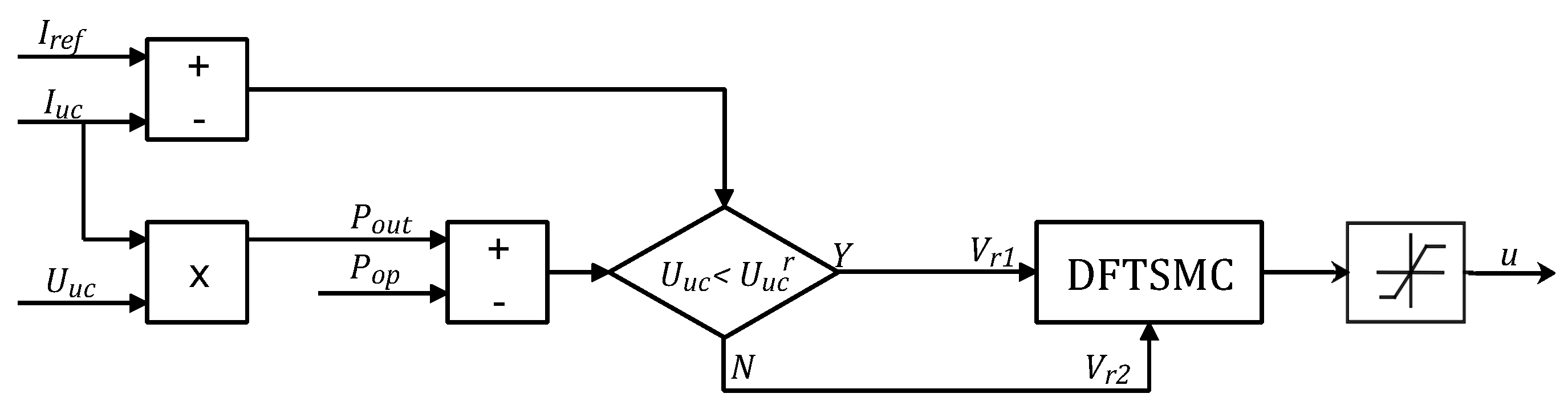
3. Discrete Fast Terminal Sliding Mode Controller Design for the Buck Converter

During the charging of the ultra-capacitor, its voltage U u c and current I u c vary in real time due to which R L constantly varies and can be derived as follows,
R L = U u c I u c
The ultra-capacitor can be charged at maximum efficiency if the system output power is equal to the optimal power, i.e., P o u t = P o p . However, if initially, U u c is too low and it is charged with high power, then it will draw an enormous amount of current, which can damage the system. To solve this issue, the charging of the ultra-capacitor is divided into two stages. The charging strategy is shown in Figure 9. In the first stage, constant current I r e f is provided to the ultra-capacitor till its voltage U u c reaches U u c r , then in the second stage, it is charged with optimal power P o p for maximum efficiency.
In order to regulate the output current ( I o u t ) and output power ( P o u t ) to the desired I r e f and P o p , respectively, a buck converter at the secondary side of the proposed system is used. The required references can be tracked by controlling the duty cycle of the switch S 5 . The circuit diagram of the buck converter is shown in Figure 3. Under the assumption that the buck converter is operating in continuous conduction mode, the following dynamic model is derived.
I ˙ L = u V a b L U o u t L
U ˙ o u t = I L C U o u t R L C
where I L and U o u t are the values of the inductor current and capacitor voltage. u = [ 0 , 1 ] is the duty ratio, used to generate the driving cycle for the switch. For the control design, we will average the model over one switching period. If x 1 is the average value of I L , x 2 is the average value of U o u t , and μ is the average value of u, then Equations (27) and (28) take the form,
x ˙ 1 = μ V a b L x 2 L
x ˙ 2 = x 1 C x 2 R L C
By controlling the output voltage of the buck converter, the output current I o u t and output power P o u t of the proposed structure can be tracked to the desired references, i.e., I r e f and P r e f , respectively.
V r 1 = I r e f R L
V r 2 = P o p R L
A discrete fast terminal sliding mode controller is designed to generate the required duty ratio for these reference voltages. For this purpose, an error signal is defined.
e 1 = x 2 V r j
where (j = 1,2). When j = 1, the controller will track constant current, and for j = 2, the controller will track constant power. By converging the e 1 to zero, we can get our desired result. The dynamic model in Equations (29) and (30) can be rewritten as,
e ˙ 1 = x ˙ 2 V ˙ r j = x 1 C x 2 R L C V ˙ r j
To simplify the expressing, a new variable e 2 is defined as,
e 2 = e ˙ 1
Taking the derivative of e 2 and using Equations (34), (29), and (30), it yields:
e ˙ 2 = 1 L C μ V a b x 2 V r j V r j x ˙ 2 R C + V ˙ r j R C V ¨ r j
The overall dynamic model can be represented as follows,
e ˙ 1 = e 2 e ˙ 2 = 1 L C μ V a b e 1 V r j + 1 R C V ˙ r j e 2 V ¨ r j
Using Euler’s discretization method, the dynamical model presented in Equation (37) can be discretized as follows,
e 1 k + 1 = e 1 k + h e 2 k e 2 k + 1 = e 2 k + h R C V ˙ r j k e 2 k h V ¨ r j k + h L C μ k V a b k e 1 k V r j k
where h is the sampling period. To converge these error signals to zero, a fast terminal sliding surface can be designed as follows,
s k = e 2 k + α 1 e 1 k + α 2 s i g n e 1 k e 1 k p q
where 0 < α 1 h < 1 , 0 < α 2 h < 1 , and 0 < p q < 1 with p and q positive odd integers. As discussed in [32], the sliding mode condition occurs when s ( k + 1 ) = 0 , and Equation (39) becomes,
s k + 1 = 0 α 2 s i g n e 1 k + 1 e 1 k + 1 p q + e 2 k + 1 + α 1 e 1 k + 1 = 0
Substituting Equation (38) into (40), it yields,
0 = e 2 k + h L C μ k V a b k e 1 k V r j k + h R C V ˙ r j k e 2 k + α 1 e 1 k + h e 2 k + α 2 s i g n e 1 k + h e 2 k e 1 k + h e 2 k p q h V ¨ r j k
Finally by solving Equation (41), the DFTSMC law can be obtained as,
u ( k ) = L C h V a b e 2 k 1 h R C + α 1 h + h V ˙ r j k R C L C h V a b e 1 k α 1 h L C h V ¨ r j k h V r j L C L C h V a b α 2 s i g n e 1 k + h e 2 k e 1 k + h e 2 k p q

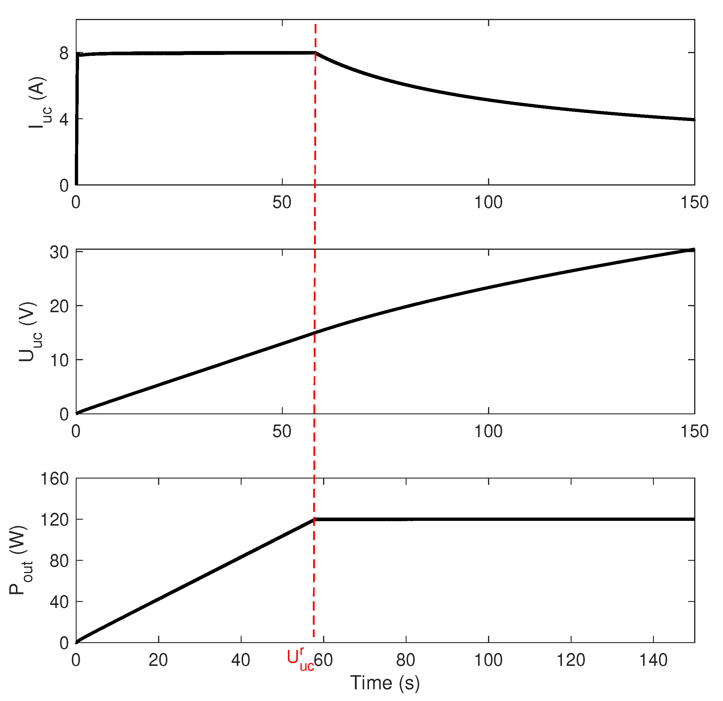
4. Results and Discussion

To verify the performance of the proposed controller, simulations were performed in MATLAB/Simulink using the “Sim Power Systems” toolbox under the abrupt and time-varying fluctuation in load R L . The uncontrolled rectifier was connected to the load through the buck converter, which was controlled by the DFTSMC. Under variations in “ R L ”, DFTSMC could regulate the output current I o u t and output power P o u t . The specifications of the wireless charging system are shown in Table 1. Using Equations (9)–(11), the parameters of the compensation network were designed and are listed in Table 2. The parameters of the buck converter and DFTSMC are listed in Table 3.
According to the charging strategy shown in Figure 9, the DFTSMC was used to generate duty cycle u to regulate the output current to the reference current, i.e., I u c = I r e f , and the output power to the optimal power P o u t = P o p . The current, voltage, and power of the ultra-capacitor are shown in Figure 10.
In the first stage, a 5 A current was tracked by the DFTSMC, and then, in the second stage, the output power was regulated to the optimal power, i.e., 120 Watts. It can be seen in Figure 11 that when the DFTSMC regulated P o u t to P o p , the R e q was regulated to R o p , i.e., 11 Ω . The duty cycle generated by the DFTSMC, during the charging process, is shown in Figure 12. The efficiency curve is shown in Figure 13, verifying that during the constant power charging stage of the ultra-capacitor, the system operated at a maximum efficiency of about 96%. During the constant power stage, the inverter output voltage and current are shown in Figure 14. According to the voltages and currents in Figure 14, the inverter output power was approximately 129 Watts, which showed that the overall efficiency from the inverter output to the load was approximately 93%.

Comparison with Other Control Schemes

To check the robustness of the DFTSMC and compare it with other control schemes such as PID and SMC, load resistance R L was changed abruptly after every 0.1 s, i.e., with a perturbation frequency of 10 Hz. The value of R L was initially set at 5 Ω, and then with a fluctuation of 40%, i.e., 2 Ω, it was decremented to 3 Ω and then incremented back to 5 Ω at 0.1 s and 0.2 s, respectively. The perturbation scheme is as follows,
R L = 5 Ω , t ϵ 0 , 0.1 s , 3 Ω , t ϵ 0.1 , 0.2 s , 5 Ω , t ϵ 0.2 , 0.3 s ,
Under the mentioned perturbations in R L , a constant output current of 5 A and constant output power of 120 Watts was tracked by the DFTSMC, sliding mode controller (SMC), and PID controller. Figure 15 shows the regulation of the output current to the referenced current, and Figure 16 shows the convergence of the output power to the referenced power, under the mentioned perturbations in R L . It can be seen that not only initially, DFTSMC tracked the required current faster, but also under the sudden variations at t = 0.1 s and 0.2 s, DFTSMC recovered quickly with respect to PID and SMC with less steady-state error. It can be observed that under these perturbations, although the PID and SMC tracked the required power, compared to DFTSMC, they exhibited initial overshoot, and comparatively, the settling time was large.

5. Experimental Validation

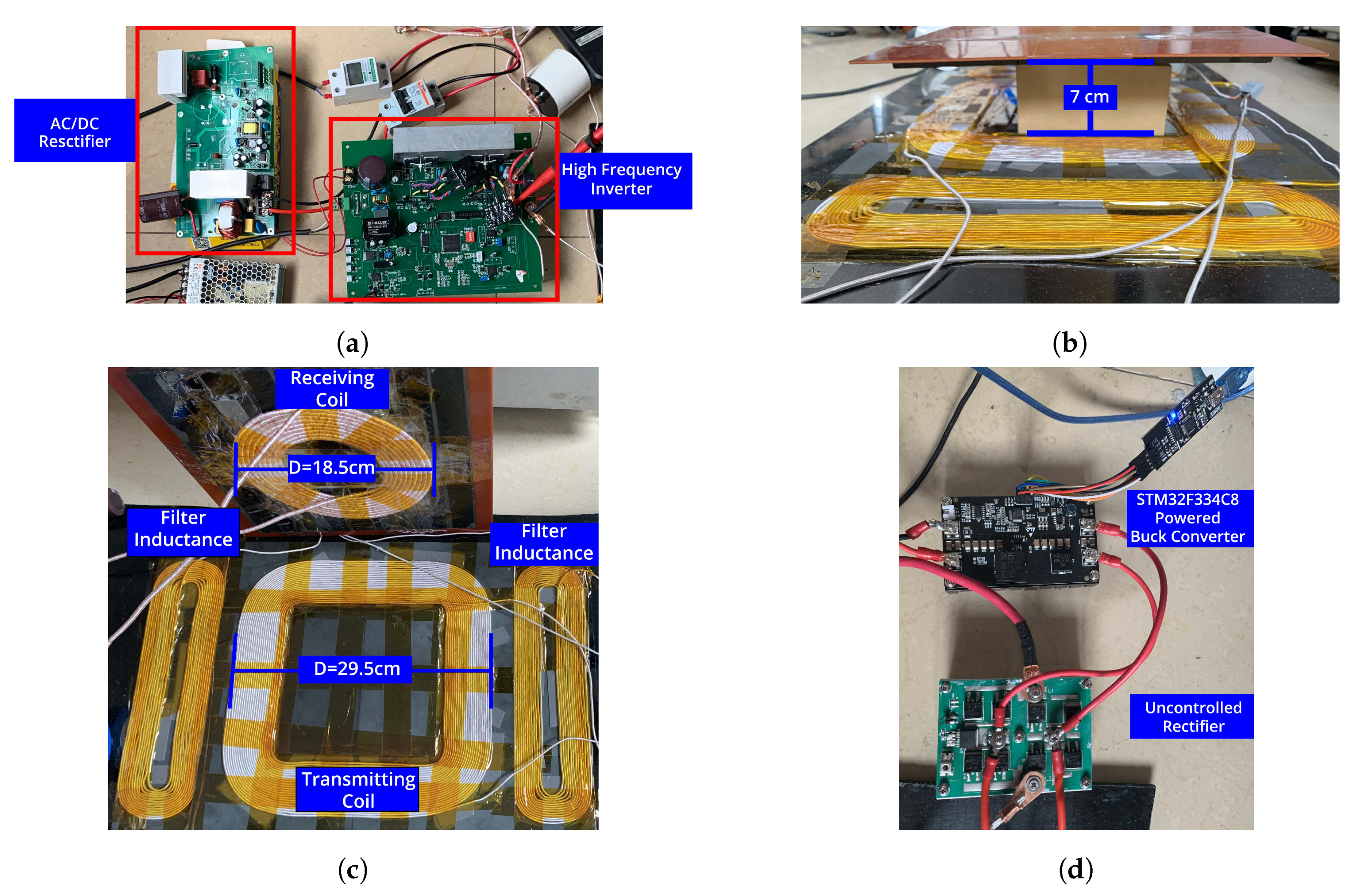
5.1. Experimental Setup
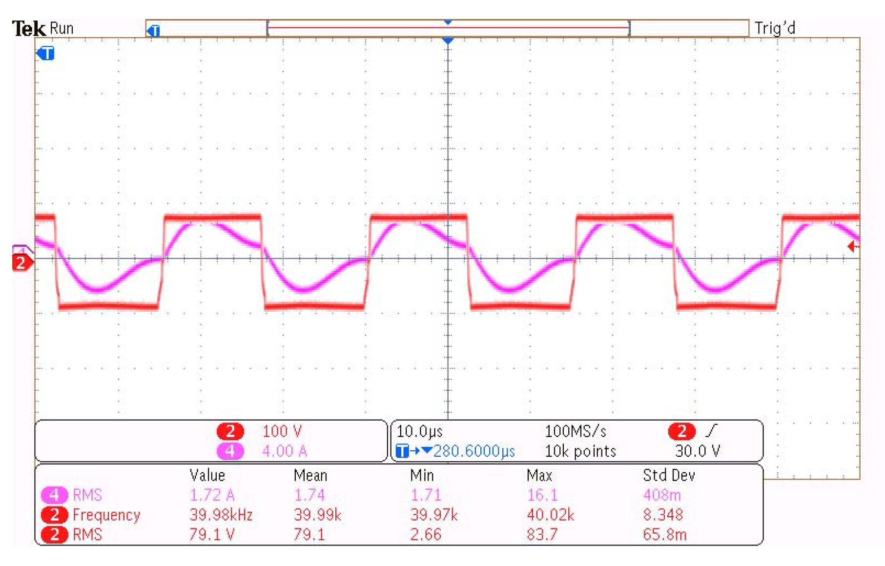
To validate the effectiveness of the proposed system, an experimental platform was fabricated. The topology of the fabricated system was similar to Figure 3, but using DC electronic load instead of the ultra-capacitor. The experiment setup is shown in Figure 17 and Figure 18. The parameters of the experimental setup are consistent with Table 1, Table 2 and Table 3. The AC/DC rectifier was used to convert the grid AC voltage into DC voltage, and the high-frequency inverter converted the DC voltage into 40 kHz AC voltage. The transmitter and receiver coils were made from tightly wound litz wire with turns of 23 and 10, respectively. The diameter of the transmitter and receiver coils was 29.5 cm and 18.5 cm, respectively, and the gap between the transmitter and receiver coils was 10 cm. The compensation elements such as filter inductance and capacitors were chosen according to the parameters listed in Table 2. The filter inductance was also made from the litz wire, designed in a DD structure to cancel out the cross-coupling effect due to the transmitter coil [33]. The buck converter was connected to the Chroma programmable DC electronic load 63200E, which was configured in constant resistance mode. The DFTSMC controller for the buck converter was implemented using the STM32F334C8 microcontroller, which generated the required PWM signals to track the constant current and power. The output current, output power, and the inverter output current and voltage were observed using the Tektronix MDO3024 Oscilloscope.

5.2. Results

To check the robustness of the proposed controller, using the programmable DC electronic load, the load resistance was abruptly changed from 5 Ω to 3 Ω and then reverted back from 3 Ω to 5 Ω . During these fluctuations, the controller was used to track the constant current of 5 A and the constant power of 120 Watts.
Figure 19 and Figure 20 show the tracking of the constant current and power, respectively. It can seen that during the fluctuations, the controller quickly recovered and tracked the required reference efficiently. Under the constant power tracking of 120 Watts, Figure 21 shows the inverter output current and voltage. According to Figure 21, the inverter output power was approximately 136 Watts, i.e., the power was transferred from the inverter to the DC Electronic load with an overall efficiency of about 88% and coupling coil efficiency of 95%. The decrease in the overall efficiency was due to losses incurred in the rectifier and buck converter. It can be seen that both the simulation and experimental data exhibited similar behavior, which validated the effectiveness of the controller in real life.

6. Conclusions

In this paper, the LCC-S topology combined with a buck converter at the secondary side was presented. The buck converter was controlled by DFTSMC to regulate the system’s output current and power. Using two-port network theory, the system was analyzed, and optimal efficiency equations were derived. Based on the analysis, the proposed system operated at maximum efficiency, when connected with optimal load, or generated optimal power. Using DFTSMC, the duty cycle of the buck converter was generated to track the required optimal power point. The simulation results verified that during charging of the ultra-capacitor, under the constant power stage, the system operated at the maximum efficiency point. The comparison with PID and SMC showed that the proposed controller overall performed better in tracking the desired current and power. Experiments were performed to validate the effectiveness of the proposed controller. The experimental results coincided with the simulation and theoretical analysis. The experimental data verified that under the abrupt perturbation in the load resistance, the controller performed well and tracked the required current and power. The future aim of this study is to model the losses incurred in the inverter, rectifier, and buck converter to analyze the effects on the system efficiency.

Author Contributions

Conceptualization, N.A. and Z.L.; formal analysis, N.A. and Z.L.; funding acquisition, Z.L. and Y.H.; investigation, Z.L. and X.W.; methodology, N.A., X.W. and H.A.; project administration, Z.L. and Y.H.; resources, Z.L. and Y.H.; software, N.A., Y.H. and H.A.; supervision, Z.L.; validation, N.A., Z.L., X.W., H.A. and A.A.; writing, original draft, N.A.; writing, review and editing, N.A., H.A. and A.A. All authors have read and agreed to the published version of the manuscript.

Funding

This research was funded by the Science and Technology Research Project of Shandong Province under Grant No. 2019GGX104080.

Conflicts of Interest

The authors declare no conflict of interest.

Abbreviations

The following abbreviations are used in this manuscript:
WPTWireless power transfer
RIPTResonant inductive power transfer
CWPTCapacitive wireless power transfer
EMRElectromagnetic radiation
AWPTAcoustic wireless power transfer
OWPTOptical wireless power transfer
SMCSliding mode controller
PIDProportional-integral-derivative
DFTSMCDiscrete fast terminal sliding mode controller
SOCState of charge
SSSeries-series
SPSeries-parallel
PSParallel-series
PPParallel-parallel
LCCinductor-capacitor-capacitor

References

  1. Tesla, N. Apparatus for Transmitting Electrical Energy. US Patent 1,119,732, 1 December 1914. [Google Scholar]
  2. Lu, X.; Wang, P.; Niyato, D.; Kim, D.I.; Han, Z. Wireless Charging Technologies: Fundamentals, Standards, and Network Applications. IEEE Commun. Surv. Tutor. 2016, 18, 1413–1452. [Google Scholar] [CrossRef] [Green Version]
  3. Barth, H.; Jung, M.; Braun, M.; Schmülling, B.; Reker, U. Concept evaluation of an inductive charging system for electric vehicles. In Proceedings of the 3rd European Conference Smart Grids and E-Mobility, Munich, Germany, 17–18 October 2011. [Google Scholar]
  4. Hui, S.Y.R.; Zhong, W.; Lee, C.K. A Critical Review of Recent Progress in Mid-Range Wireless Power Transfer. IEEE Trans. Power Electron. 2014, 29, 4500–4511. [Google Scholar] [CrossRef] [Green Version]
  5. Lu, X.; Niyato, D.; Wang, P.; Kim, D.I.; Han, Z. Wireless charger networking for mobile devices: Fundamentals, standards, and applications. IEEE Wirel. Commun. 2015, 22, 126–135. [Google Scholar] [CrossRef] [Green Version]
  6. Tang, Y.; Chen, Y.; Madawala, U.K.; Thrimawithana, D.J.; Ma, H. A New Controller for Bidirectional Wireless Power Transfer Systems. IEEE Trans. Power Electron. 2018, 33, 9076–9087. [Google Scholar] [CrossRef]
  7. Lu, F.; Zhang, H.; Mi, C. A Two-Plate Capacitive Wireless Power Transfer System for Electric Vehicle Charging Applications. IEEE Trans. Power Electron. 2018, 33, 964–969. [Google Scholar] [CrossRef]
  8. RamRakhyani, A.K.; Mirabbasi, S.; Chiao, M. Design and Optimization of Resonance-Based Efficient Wireless Power Delivery Systems for Biomedical Implants. IEEE Trans. Biomed. Circuits Syst. 2011, 5, 48–63. [Google Scholar] [CrossRef] [PubMed]
  9. Xue, R.; Cheng, K.; Je, M. High-Efficiency Wireless Power Transfer for Biomedical Implants by Optimal Resonant Load Transformation. IEEE Trans. Circuits Syst. I Regul. Pap. 2013, 60, 867–874. [Google Scholar] [CrossRef]
  10. Mashhadi, I.A.; Pahlevani, M.; Hor, S.; Pahlevani, H.; Adib, E. A New Wireless Power Transfer Circuit for Retinal Prosthesis. IEEE Trans. Power Electron. 2019, 34, 6425–6439. [Google Scholar] [CrossRef]
  11. Zhang, Y.; Zhao, Z.; Chen, K. Frequency Decrease Analysis of Resonant Wireless Power Transfer. IEEE Trans. Power Electron. 2014, 29, 1058–1063. [Google Scholar] [CrossRef]
  12. Roes, M.G.; Duarte, J.L.; Hendrix, M.A.; Lomonova, E.A. Acoustic energy transfer: A review. IEEE Trans. Ind. Electron. 2012, 60, 242–248. [Google Scholar] [CrossRef]
  13. Dai, J.; Ludois, D.C. Wireless electric vehicle charging via capacitive power transfer through a conformal bumper. In Proceedings of the 2015 IEEE Applied Power Electronics Conference and Exposition (APEC), Charlotte, NC, USA, 15–19 March 2015; pp. 3307–3313. [Google Scholar] [CrossRef]
  14. Dai, H.; Liu, Y.; Chen, G.; Wu, X.; He, T.; Liu, A.X.; Ma, H. Safe Charging for Wireless Power Transfer. IEEE/ACM Trans. Netw. 2017, 25, 3531–3544. [Google Scholar] [CrossRef]
  15. Dickinson, R.M. Wireless power transmission technology state of the art the first Bill Brown lecture. Acta Astronaut. 2003, 53, 561–570. [Google Scholar] [CrossRef]
  16. Sahai, A.; Graham, D. Optical wireless power transmission at long wavelengths. In Proceedings of the 2011 International Conference on Space Optical Systems and Applications (ICSOS), Santa Monica, CA, USA, 11–13 May 2011; pp. 164–170. [Google Scholar]
  17. Tseng, V.F.-G.; Bedair, S.S.; Lazarus, N. Phased array focusing for acoustic wireless power transfer. IEEE Trans. Ultrasonics Ferroelectrics Frequency Control. 2017, 65, 39–49. [Google Scholar] [CrossRef] [PubMed]
  18. Awal, M.R.; Jusoh, M.; Sabapathy, T.; Kamarudin, M.R.; Rahim, R.A. State-of-the-art developments of acoustic energy transfer. Int. J. Antennas Propag. 2016, 2016, 3072528. [Google Scholar] [CrossRef] [Green Version]
  19. Li, S.; Mi, C.C. Wireless power transfer for electric vehicle applications. IEEE J. Emerg. Sel. Top. Power Electron. 2015, 3, 4–17. [Google Scholar]
  20. Qiu, C.; Chau, K.T.; Ching, T.W.; Liu, C. Overview of wireless charging technologies for electric vehicles. J. Asian Electr. Veh. 2014, 12, 1679–1685. [Google Scholar] [CrossRef] [Green Version]
  21. Wang, C.S.; Stielau, O.H.; Covic, G.A. Design considerations for a contactless electric vehicle battery charger. IEEE Trans. Ind. Electron. 2005, 52, 1308–1314. [Google Scholar] [CrossRef]
  22. Kalwar, K.A.; Mekhilef, S.; Seyedmahmoudian, M.; Horan, B. Coil design for high misalignment tolerant inductive power transfer system for EV charging. Energies 2016, 9, 937. [Google Scholar] [CrossRef] [Green Version]
  23. Cirimele, V.; Freschi, F.; Guglielmi, P. Wireless power transfer structure design for electric vehicle in charge while driving. In Proceedings of the 2014 International Conference on Electrical Machines (ICEM), Berlin, Germany, 2–5 September 2014; pp. 2461–2467. [Google Scholar]
  24. Spanik, P.; Frivaldsky, M.; Drgona, P.; Jaros, V. Analysis of proper configuration of wireless power transfer system for electric vehicle charging. In Proceedings of the ELEKTRO 2016, Strbske Pleso, Slovakia, 16–18 May 2016; pp. 231–237. [Google Scholar]
  25. Geng, Y.; Li, B.; Yang, Z.; Lin, F.; Sun, H. A high efficiency charging strategy for a supercapacitor using a wireless power transfer system based on inductor/capacitor/capacitor (LCC) compensation topology. Energies 2017, 10, 135. [Google Scholar] [CrossRef]
  26. Li, H.; Li, J.; Wang, K.; Chen, W.; Yang, X. A maximum efficiency point tracking control scheme for wireless power transfer systems using magnetic resonant coupling. IEEE Trans. Power Electron. 2014, 30, 3998–4008. [Google Scholar] [CrossRef]
  27. Li, B.; Geng, Y.; Lin, F.; Yang, Z.; Igarashi, S. Design of constant voltage compensation topology applied to wpt system for electrical vehicles. In Proceedings of the 2016 IEEE Vehicle Power and Propulsion Conference (VPPC), Hangzhou, China, 17–20 October 2016; pp. 1–6. [Google Scholar]
  28. Li, Z.; Zhu, C.; Jiang, J.; Song, K.; Wei, G. A 3-kW wireless power transfer system for sightseeing car supercapacitor charge. IEEE Trans. Power Electron. 2016, 32, 3301–3316. [Google Scholar] [CrossRef]
  29. Zhong, W.; Hui, S. Maximum energy efficiency tracking for wireless power transfer systems. IEEE Trans. Power Electron. 2014, 30, 4025–4034. [Google Scholar] [CrossRef] [Green Version]
  30. Yang, Y.; Zhong, W.; Kiratipongvoot, S.; Tan, S.C.; Hui, S.Y.R. Dynamic improvement of series–series compensated wireless power transfer systems using discrete sliding mode control. IEEE Trans. Power Electron. 2017, 33, 6351–6360. [Google Scholar] [CrossRef]
  31. Huangfu, Y.; Zhuo, S.; Rathore, A.; Breaz, E.; Nahid-Mobarakeh, B.; Gao, F. Super-twisting differentiator-based high order sliding mode voltage control design for DC-DC buck converters. Energies 2016, 9, 494. [Google Scholar] [CrossRef] [Green Version]
  32. Xu, J.-X.; Abidi, K. Output Tracking with Discrete-Time Integral Sliding Mode Control. In Modern Sliding Mode Control Theory: New Perspectives and Applications; Bartolini, G., Fridman, L., Pisano, A., Usai, E., Eds.; Springer: Berlin/Heidelberg, Germany, 2008; pp. 247–268. [Google Scholar]
  33. Lu, F.; Zhang, H.; Hofmann, H.; Su, W.; Mi, C.C. A dual-coupled LCC-compensated IPT system with a compact magnetic coupler. IEEE Trans. Power Electron. 2017, 33, 6391–6402. [Google Scholar] [CrossRef]
Figure 1. Typical RIPT WPT system.
Energies 13 01370 g001
Figure 2. Basic compensation networks (a) series-series, (b) parallel-series, (c) series-parallel, and (d) parallel-parallel.
Energies 13 01370 g002
Figure 3. Circuit diagram of the proposed WPT system.
Energies 13 01370 g003
Figure 4. Equivalent diagram of proposed system.
Energies 13 01370 g004
Figure 5. Two port network of the proposed system.
Energies 13 01370 g005
Figure 6. (a) Mode 1: Load is disconnected. (b) Mode 2: Input source is disconnected.
Energies 13 01370 g006
Figure 7. Efficiency, η vs. R e q .
Energies 13 01370 g007
Figure 8. Efficiency, η vs. P o u t .
Energies 13 01370 g008
Figure 9. Charging strategy for the ultra-capacitor.
Energies 13 01370 g009
Figure 10. Current, voltage, and power of the ultra-capacitor.
Energies 13 01370 g010
Figure 11. Equivalence resistance of the system.
Energies 13 01370 g011
Figure 12. Duty cycle during the charging process.
Energies 13 01370 g012
Figure 13. WPT system efficiency during charging process.
Energies 13 01370 g013
Figure 14. Inverter output voltage and current.
Energies 13 01370 g014
Figure 15. Regulation of output current, I o u t , during perturbation in R L .
Energies 13 01370 g015
Figure 16. Regulation of output Power, P o u t , during perturbation in R L .
Energies 13 01370 g016
Figure 17. Experimental setup.
Energies 13 01370 g017
Figure 18. (a) AC/DC rectifier and high-frequency inverter. (b) Transmitting and receiving coils’ gap. (c) Transmitting and receiving coils. (d) Uncontrolled rectifier and buck converter.
Energies 13 01370 g018
Figure 19. Tracking of constant current.
Energies 13 01370 g019
Figure 20. Tracking of constant power.
Energies 13 01370 g020
Figure 21. Inverter output voltage and current.
Energies 13 01370 g021
Table 1. Wireless charger parameters.
SymbolParameterValue
V i n Input voltage80 V
L 1 Transmitting coil inductance400 μH
R 1 Transmitting coil resistance∼300 mΩ
L 2 Receiving coil inductance30 μH
R 2 Receiving coil resistance∼120 mΩ
MMutual inductance60 μH
f s Switching frequency40 kHz
P o Output power120 Watts
I o Output current5 A
Table 2. Compensation network parameters.
SymbolParameterValue
L f 1 Transmitting side compensation inductance135 μH
C f 1 Transmitting side parallel compensation capacitance0.117 μF
C 1 Transmitting side series compensation capacitance0.059 μF
R f 1 Transmitting side compensation inductor resistance200 mΩ
C 2 Receiving side series compensation capacitance0.52 μF
Table 3. Buck converter and DFTSMC parameters.
SymbolParameterValue
LInductor5 mH
CCapacitor500 μF
α 1 Constant500
α 2 Constant3000
hSampling period1 ms

