Article

Electrical Characterization of MIS Schottky Barrier Diodes Based on Nanostructured Porous Silicon and Silver Nanoparticles with Applications in Solar Cells

by
Rehab Ramadan
1,2,* and
Raúl J. Martín-Palma
1,3
1
Departamento de Física Aplicada, Universidad Autónoma de Madrid, 28049 Madrid, Spain
2
Department of Physics, Faculty of Science, Minia University, Minia 61519, Egypt
3
Instituto Universitario de Ciencia de Materiales “Nicolás Cabrera”, Universidad Autónoma de Madrid, 28049 Madrid, Spain
*
Author to whom correspondence should be addressed.
Submission received: 25 March 2020 / Revised: 17 April 2020 / Accepted: 23 April 2020 / Published: 1 May 2020
(This article belongs to the Section A2: Solar Energy and Photovoltaic Systems)

Abstract

:
The accurate determination of the electrical properties of photovoltaic devices is of utmost importance to predict and optimize their overall optoelectronic performance. For example, the minority carrier lifetime and the carrier diffusion length have a strong relationship with the carrier recombination rate. Additionally, parasitic resistances have an important effect on the fill factor of a solar cell. Within this context, the alternating current (AC) and direct current (DC) electrical characteristics of Si-based metal–insulator–semiconductor (MIS) Schottky barrier diodes with the basic structure Al/Si/TiO2/NiCr were studied, aiming at using them as photovoltaic devices. The basic diode structure was modified by adding nanostructured porous silicon (nanoPS) layers and by infiltrating silver nanoparticles (AgNPs) into the nanoPS layers, leading to Al/Si+nanoPS/TiO2/NiCr and Al/Si+nanoPS+AgNPs/TiO2/NiCr structures, respectively. The AC electrical properties were studied using a combination of electrochemical impedance spectroscopy and Mott–Schottky analysis, while the DC electrical properties were determined from current–voltage measurements. From the experimental results, an AC equivalent circuit model was proposed for the three different MIS Schottky barrier diodes under study. Additionally, the most significant electrical parameters were calculated. The results show a remarkable improvement in the performance of the MIS Schottky barrier diodes upon the addition of hybrid nanoPS layers with embedded Ag nanoparticles, opening the way to their use as photovoltaic devices.

Graphical Abstract

1. Introduction

During the past few years, there has been a great interest towards the integration of nanostructured porous silicon (nanoPS) with silicon micro- and optoelectronic devices [1,2]. For applications in these fields, including as photodiodes and solar cells, the efficiency and performance of the electrical contacts to nanoPS is a key factor. In particular, it is of great importance to determine the specific mechanisms of carrier transport, since these will play a crucial role in the performance of nanoPS-based devices. Previous low-temperature DC studies of metal/nanoPS/Si structures showed rectifying behavior, and the subsequent analysis of their current-voltage (I-V) characteristics allowed identification of them as metal–insulator–semiconductor (MIS) Schottky junctions [3,4].
MIS Schottky junctions have found important applications in the broad fields of micro- and optoelectronics, including diodes [5], near-infrared (NIR) photodetectors [6], photoelectrochemical water oxidation devices [7], and photovoltaic solar cells [8]. In the particular case of Schottky barrier solar cells, the presence of an insulator thin film avoids the principal shortcoming of metal–semiconductor (MS) Schottky barriers, which is their typically low open-circuit voltage, Voc [9]. In fact, it has been found by several authors that the use of MIS junctions results in increased Voc, compared to that of MS Schottky barrier solar cells [10,11,12,13]. This increase in Voc leads to (1) decreased reverse saturation current density associated with thermionic emission in the Schottky barrier, (2) increased value of the diode ideality factor, and/or (3) increased effective Schottky barrier height [14]. In fact, the key transport mechanisms of MIS Schottky barrier diodes are tunneling through the insulator or the interfacial layer by the majority carriers or diffusion current due to the minority carriers [15,16]. This effect is drastically manifested in nanoPS, given its high specific surface area.
A thorough study of the AC and DC electrical properties of MIS Schottky barrier diodes is essential to understand their fundamental electrical conduction properties. In this line, electrochemical impedance spectroscopy (EIS) enables determination of the electrical parameters which characterize the electrical conduction properties of the interfaces of a device in a given frequency range [17]. EIS has been previously used to investigate the internal electrical properties of the interfaces of multilayer structures, such as light-emitting diodes [18], electrochromic smart windows [19,20], Li+-ion batteries, [21] and photovoltaic devices [17], by establishing an equivalent circuit model. Capacitance-voltage (C-V) characterization at a fixed frequency allows evaluation of other essential electrical parameters. Within this context, the Mott–Schottky model [22] allows determination of the built-in potential, semiconductor type, and doping density. Since not all the electrical conduction parameters for a given device can be obtained from EIS and C-V measurements, DC current–voltage (I-V) analysis provides some additional semiconductor device electrical parameters, including diffusion and recombination currents in dark and bulk resistances [23].
The main aim of the present work is to study the AC and DC electrical conduction properties of three different Si-based MIS Schottky barrier diodes to assess their potential use in the field of photovoltaics. The optoelectronic properties of similar structures were recently studied [24]. The basic structure of the MIS Schottky barrier devices is Al/Si/TiO2/NiCr, with the Al/Si interface behaving as an ohmic contact. A variation of the basic device includes a nanoPS layer grown on the Si substrate, leading to diodes with the structure Al/Si+nanoPS/TiO2/NiCr. The last modification includes a layer consisting of silver nanoparticles (AgNPs) embedded into nanoPS, resulting in the structure Al/Si+nanoPS+AgNPs/TiO2/NiCr. The AC electrical properties were determined using a combination of EIS and C-V measurements, while the DC electrical properties were obtained from I-V measurements. From the experimental EIS results, an AC equivalent circuit model was proposed for the three different MIS Schottky devices, and the internal resistance and capacitance associated to each interface were calculated. Additionally, both the minority carrier lifetimes and minority carrier diffusion coefficients were calculated. From the C-V results at fixed frequencies, the built-in potential, doping concentration, and the type of the semiconductor were determined. Finally, the reverse saturation current, ideality factor, parasitic resistances, and built-in potential were obtained from the experimental I-V data.

2. Experimental

2.1. Fabrication of the Si-Based MIS Schottky Barrier Diodes

2.1.1. Fabrication of the NanoPS Layers

Low-resistivity ohmic back contacts to boron-doped (p-type) silicon wafers (100) orientation and resistivity of 25–30 Ω·cm) were fabricated by electron beam evaporation of 150 nm-thick Al layers and subsequent thermal annealing in a nitrogen atmosphere for 5 min. The Si wafers were cut into 1.5 × 1.5 cm2 pieces, each of which were mounted in a sample holder and exposed to the etching solution, consisting of a 1:6 HF (48 wt%):dimethyl formamide (99 wt%) mixture. The native oxide layer was removed before starting the etching process by immersing, for 60 s, the Si pieces in a HF:H2O (1:20) solution. The anodization process was carried out under an applied current density of 10 mA/cm2 and a fixed anodization time of 120 s, leading to nanoPS layers with thickness of around 120 nm. Once the etching process was completed, the nanoPS layers grown onto Si were cleaned with ethanol to remove any residuals from the HF solution, and finally blown dry with a mild stream of dry nitrogen. The experimental setup of the anodization process has previously been described and is schematically presented in [25].

2.1.2. Infiltration of Silver Nanoparticles (AgNPs)

Silver nanoparticles (AgNPs) were grown inside the nanoPS layers using an electrochemical deposition process described in previous work [25]. An aqueous solution of silver nitrate, sodium citrate, and nitric acid (pH = 3) was used. The current density was, in all cases, 1 µA/cm2 and the infiltration time was 4 min. The electrochemical deposition process led to the formation of hybrid layers composed of nanoPS and silver nanoparticles (nanoPS+AgNPs).

2.1.3. Spin Coating of TiO2 Thin Films

A solution of titanium isopropoxide (Ti[OCH(CH3)2]4) in ethanol was prepared with a 0.4 M concentration. Afterwards, 115 μL of HCl acid was added to the solution to induce an acid catalysis to prevent nanoPS from damage. The solution was stirred at 3000 rpm at room temperature for 30 min to obtain a clear solution. A total of 60 μL of the solution was cast on either the Si substrate, the nanoPS layers, or the nanoPS+AgNPs hybrid layers at a spinning speed of 3000 rpm for 30 s. Finally, the resulting TiO2 thin films were annealed on a hot plate at 150 °C for 5 min to evaporate the remaining solvents.

2.1.4. Ni/Cr Top Contact

Electron beam evaporation was used to deposit 100 nm-thick Ni/Cr (80%/20%) top contacts on the TiO2 thin films. The base pressure was 2.5 × 10⁻⁵ mbar, and the evaporation time was 5 min. A metallic mask was used to define the geometry at the microscale of the Ni/Cr front contacts. The area was 0.15 cm2.
Figure 1 shows the final structure of the Al/Si+nanoPS+AgNPs/TiO2/NiCr Schottky barrier diodes. In addition to this basic device, two other Schottky barrier diodes were fabricated to compare their performance, namely Al/Si/TiO2/NiCr and Al/Si+nanoPS/TiO2/NiCr.
In summary, the structure of the three different Si-based MIS Schottky barrier diodes analyzed in this work is Al/active layer/TiO2/NiCr, the active layer being respectively Si, Si+nanoPS, or Si+nanoPS+AgNPs. Therefore, the electrical conduction properties of the different active layers are expected to have a pivotal role in the overall performance of the diodes.

2.2. Characterization

The morphologies of the different layers and interfaces were analyzed by field emission scanning electron microscopy (XL-40 FEG, Philips, Eindhoven, The Netherlands) operated at 5 kV.
Alternating current (AC) and direct current (DC) electrical measurements were carried out using a potentiostat instruments (SP-150, BioLogic, Seyssinet-Pariset, France).
For electrochemical impedance spectroscopy (EIS) measurements, a voltage amplitude of 500 mV and a frequency range between 1 Hz and 1 MHz were used. Capacitance-voltage (C-V) characterization was performed at three specific frequencies, 1 KHz, 5 KHz, and 10 KHz, under reverse bias from 0 V to −1 V with a scan rate of 20 mV/s. For current–voltage (I-V) measurements, the applied potential was varied between −1.5 and +1.5 V, and the scan rate was set at 5 mV/s. All the measurements were carried out at room temperature in a Faraday cage to shield the electrical measurements from any external signals.

3. Experimental Results

3.1. Morphology

Typical field emission scanning electron microscopy (FESEM) images of the nanoPS layers after the electrochemical deposition of Ag nanoparticles (AgNPs) are presented in Figure 2a,b. These images confirm the infiltration of these nanoparticles inside the pores. It was determined that the diameter of the AgNPs typically ranges between 5 and 15 nm. Figure 2c,d portray cross-sectional and top views of characteristic nanoPS+AgNPs layers coated with a very thin layer of TiO2. The images confirm the extremely small thickness of the TiO2 layer ( ~ 10   nm ) , given the notable conformality observed.

3.2. Electrical Characterization

3.2.1. AC Electrical Measurements

EIS analysis, given its power and versatility, was used to determine the electrical transport properties through the interfaces of the three different Si-based MIS Schottky diodes. From the fitting of the Nyquist plots (Figure 3), a full equivalent circuit model for these devices was proposed. The equivalent circuit, which includes an intricate combination of resistances (R), capacitors (C), and a constant phase element (Q), is depicted in Figure 4. For the interpretation of the results, it must be kept in mind that resistance is a parameter which is strongly related to the carrier transport properties, while capacitance is linked to the carrier accumulation and distribution and to the presence of defect traps [17]. Furthermore, a constant phase element (CPE) is a circuit element that models an imperfect capacitor. The “anomalous” capacitive behavior is generally attributed to thickness and/or composition inhomogeneity, leading to variations in conductivity, and/or to roughness at the interfaces [26]. Thus, its characteristic capacitance, C, can be calculated with the following equation [27]:
C = Q 1 a · R 1 a a
where Q is the CPE and the factor a is an index which indicates the degree of “perfection” of this element. This index can vary between 0 and 1, with 0 describing a perfect resistor, and 1 a perfect capacitor [26]. The differences in the impedance of the interfaces of the three MIS Schottky barrier diodes analyzed in this work will be analyzed in the following paragraphs.
Figure 3 shows the Nyquist plots for the three MIS Schottky barrier diodes, i.e., Al/Si/TiO2/NiCr, Al/Si+nanoPS/TiO2/NiCr, and Al/Si+nanoPS+AgNPs/TiO2/NiCr. As each MIS structure has three different interfaces, every interface has been attributed to a semicircle in the corresponding Nyquist plot so that each semicircle is associated to an individual electrical transport process. Table 1 summarizes the interfaces under study for the three Si-based Schottky diodes.
The best fitting of the equivalent circuit for the three Si-based devices was obtained using a series resistance and three parallel resistor-capacitor (RC) circuits, as shown in Figure 4, where each RC circuit shows a semicircle in the Nyquist plots portrayed in Figure 3. The semicircle present at low frequencies is attributed to the Al/active layer interface (1st interface), while the semicircle at mid frequencies is associated to the active layer/TiO2 interface (2nd interface). The last semicircle, observed at high frequencies, is attributed to the TiO2/NiCr interface (3rd interface). It must be pointed out that for the Al/Si+nanoPS/TiO2/NiCr Schottky barrier diodes, the active layer is just represented by one semicircle, given that we assume that there are no rectifying interfaces between Si and nanoPS. In this regard, we consider that this is a heterostructure formed between two p-type semiconductors with different bandgaps, the bandgap of nanoPS being larger than that of Si [28,29]. It is also important to notice that electrical conduction through nanoPS is much lower than through Si, which is attributed to their very different conductivities [30,31]. What is more, since the silver nanoparticles do not form a continuous layer (as shown in Figure 2), we assume that the Si+nanoPS+AgNPs structure also represents just one active layer.
Table 2 portrays a comparison between the RC elements for the interfaces of each device. Due to the very different active layer for each device, the electrical RC parameters are rather dissimilar. It is observed that for the three active layer/TiO2 interfaces, the electrical conduction of the Al/Si+nanoPS/TiO2/NiCr devices is lower than that of the Al/Si/TiO2/NiCr devices, most likely due to the formation of the nanopores in the heavily-doped regions of the Si substrate, leading to an effective reduction of the doping concentration [29]. The experimental results also show that the electrical conduction is notably increased in the devices based on nanoPS combined with metallic Ag nanoparticles. This behavior is attributed to increased electrical conduction due to the presence of the AgNPs embedded into the nanoPS layers. A comparable enhancement in the electrical conduction of silica nanofiber structures was recently observed upon incorporation of gold nanoparticles [32].
Additionally, the changes in the structure of the active layer could have an important effect on the electrical conduction properties of all the interfaces of the devices. The electrical conduction for the interface’s Al/active layer and TiO2/NiCr decreases for the Al/Si/TiO2/NiCr devices, due to the large thickness of the TiO2 thin films. Also, the reduction for the Al/Si+nanoPS/TiO2/NiCr devices is attributed to the lower conduction of nanoPS, compared to Si. However, the improved conduction for the Al/Si+nanoPS+AgNPs/TiO2/NiCr devices is attributed to the combination of the nanoPS and metallic nanoparticles.
The minority carrier lifetime (τ) for every interface can be obtained from the well-known relationship [33]:
τ = R C
where R is the electrical resistance and C is the electrical capacitance at each interface. The results are compiled in Table 2. It can be observed that the Al/Si+nanoPS+AgNPs/TiO2/NiCr device shows the lowest values for τ1, τ2, and τ3, which are associated with increased conduction. The observed increase in τ1, τ2, and τ3 for the Al/Si/TiO2/NiCr devices is related to the large thickness of the TiO2 thin films and the large carrier recombination rates of Si [34], as previously indicated in the analysis of the Nyquist plots. The values obtained for τ1, τ2, and τ3 for the Al/Si+nanoPS/TiO2/NiCr devices are attributed to conduction losses associated with the porous structure of the nanoPS layers, as well as with the formation of defects on their surface [35]. The combination of the nanoPS layers with metallic nanoparticles has a notable effect on the electrical conduction at the active layer/TiO2 interfaces, which leads to a small value of τ2. More specifically, τ2 decreases from 3.09 µs for the Al/Si+nanoPS/TiO2/NiCr devices to 0.03 µs for the Al/Si+nanoPS+AgNPs/TiO2/NiCr devices.
Table 2 shows that C1 and C2 are lower for the Al/Si+nanoPS/TiO2/NiCr devices than for the Al/Si/TiO2/NiCr devices. The observed decrease in the capacitance at the two nanoPS interfaces could be due to the particular structure of the nanoPS layers, which would induce quite large leakage currents. However, at the TiO2/NiCr interface, the capacitance increased from 19.7 nF for the Al/Si/TiO2/NiCr devices to 31.5 nF for the Al/Si+nanoPS/TiO2/NiCr devices. This variation could be due to a more homogeneous TiO2 thin film when grown on the nanoPS layers, as discussed above.
The minority carrier diffusion coefficient can be calculated using the thickness of the interfaces (L) and τ, by means of the following relationship [36]:
D = L 2 τ
Since the smallest values for τ are obtained for the Al/Si+nanoPS+AgNPs/TiO2/NiCr Schottky devices, D will show the largest values. A higher diffusion coefficient indicates a larger average length for a carrier between generation and recombination [33]. These results are further confirmed by the improvement of the optoelectronic performance of the Al/Si+nanoPS+AgNPs/TiO2/NiCr devices, as demonstrated in a previous work [24].
Figure 5 shows the Bode diagrams for the three Si-based MIS Schottky barrier diodes analyzed in this work. These curves allow studying of the variation of the impedance with frequency in the 1 Hz to 1 MHz range. The experimental results show that, in all cases, the impedance is approximately constant in the low frequency range, while a notable reduction with increasing frequency (1 KHz to 1 MHz) is observed. The inverse relation between impedance and frequency is attributed to a parallel configuration of RC elements. The impedance of a parallel RC circuit is given by the following equation [37]:
1 Z = 1 R + 1 X c ,                           X c = 1 2 π f C
where XC is the capacitive reactance in Ohms, ƒ is the frequency in Hertz, and C is the AC capacitance in Farads. From that, the capacitive reactance itself is inversely proportional to the applied frequency.
Mott–Schottky analysis allows determination of several parameters of semiconductors, such as the flat-band potential, carrier doping density, and the type of the semiconductor. Aiming at determining these parameters, C-V measurements were recorded at the three specific frequencies where the impedance shows a noticeable change with frequency in the Bode plot, namely 1, 5, and 10 kHz. From the experimental values, the Mott–Schottky plots shown in Figure 6, Figure 7, and Figure 8 were generated for the three MIS Schottky barrier devices. The AC electrical parameters were calculated using the Mott–Schottky equation [38]:
1 C 2 = 2 ( ε ε 0 A 2 q N D ) ( V V f b K B T q )
where C (F) is the space charge capacitance, A (cm2) the active geometric area, ND (cm−3) the semiconductor doping density, q the electron charge (1.602 × 10⁻¹⁹ C), ε the relative permittivity (19.8 for p-type silicon), ε0 the vacuum permittivity (8.854 × 10⁻¹² F·m−1), V (V) the applied potential, V f b the flat-band potential, at which there is no band bending or field inside the semiconductor [22], KB is the Boltzmann constant (1.381 × 10⁻²³ J·K−1), and T the absolute room temperature.
The negative slope of the straight line from the three C−2-V plots confirms the p-type character of the electrical conductivity in all cases. According to Equation (5), the intercept of this straight line to the voltage axis gives the value of the flat-band potential, while the carrier concentration can be calculated from the value of the slope. The built-in potential (Vbi) can be determined from the flat-band potential, according to the following equation [39]:
V b i = V f b K B T q
All the Mott–Schottky diagrams confirm the decrease of capacitance with increasing frequency in the 1 KHz to 10 KHz range. Likewise, in all cases, the flat-band potential decreases with increasing frequency. Since all the MIS Schottky barrier devices have the same behavior with frequency, the results at 1 KHz are compared in Table 3. The values for Vbi, which opposes the flow of the carriers across the junction, slightly decreased in the case of the Al/Si+nanoPS/TiO2/NiCr devices, in comparison with the Al/Si/TiO2/NiCr devices. This reduction is attributed to the wider band gap of the nanoPS structures, compared to Si [28]. It is also observed that ND decreased from 0.617 × 1015 cm−3 for the Al/Si/TiO2/NiCr devices to 0.121 × 1015 cm−3 for the Al/Si+nanoPS/TiO2/NiCr devices, probably due to the formation of a porous Si layer in the heavily-doped regions of the Si substrate [28]. For the Al/Si+nanoPS+AgNPs/TiO2/NiCr devices, a remarkable decrease in Vbi from 0.515 V for the Al/Si/TiOx/NiCr devices to 0.115 V for the Al/Si+nanoPS+AgNPs/TiO2/NiCr devices is observed. The notable decrease in Vbi for the Al/Si+nanoPS+AgNPs/TiO2/NiCr devices is probably due to the improvement of the electrical RC parameters, which is indicative of low τ and large D, as determined from EIS measurements. An improvement in the electrical conduction has also been demonstrated through the values calculated for the carrier doping concentration, which were 0.61 × 1015 cm−3 for the Al/Si/TiO2/NiCr devices, and notably increased to 8.6 × 1015 cm−3 for the Al/Si+nanoPS+AgNPs/TiO2/NiCr devices.

3.2.2. DC Electrical Measurements

Current-voltage (I-V) measurements of Schottky barrier devices can be used to determine some of their essential parameters, which allows for describing and optimizing their overall performance. This study is aimed at determining the reverse saturation current (I0), diode ideality factor (n), parasitic series (Rs) and shunt resistances (Rsh), and barrier height (φB). Figure 9 portrays the experimental I-V curves in the −1.5 V to +1.5 V range for the three Schottky barrier devices. The experimental results confirm the rectifying behavior for all the devices, which is consistent with a thermionic emission carrier transport mechanism, with a variation in the particular values of the reverse saturation current in the dark.
An ideal diode has low resistance (ideally zero) under forward bias, and high resistance (ideally infinite) under reverse bias. The Schottky ideal diode equation is given by [40]:
I D = I 0 [ e q V n K B T 1 ]
where I D is the current in the dark, I0 is the reverse saturation current, n is the diode ideality factor (equal to one for a Si ideal diode and 2 for Ge), KB is the Boltzmann constant, and T is the absolute junction temperature. The ideal diode equation assumes that all recombination processes occur via band-to-band transitions or through traps in the bulk of the device. However, recombination could occur in other areas of the device, leading to losses in the overall performance of the diode. As such, a modified equation widely used for non-ideal diodes is given by the expression [40]:
I D = I 0 [ e q ( V I R s ) n K B T 1 ] + V I R s R s h
Large values of Rs cause power to be dissipated in solar cells, while low Rsh leads to power losses by providing an alternate current path for the light-generated current.
The Al/Si/TiO2/NiCr devices show the lowest values of ID, probably as a consequence of coating the Si substrates with a compact and continuous interfacial thin film of TiO2, which acts as a very effective insulating thin film. To analyze the effect of the TiO2 thin film on the reduction in the current through the device, the inset of Figure 9 shows the I-V curve corresponding to the Al/Si/TiO2/NiCr devices without TiO2 layer. The Al/Si+nanoPS/TiO2/NiCr devices show larger ID values than those of the Al/Si/TiO2/NiCr devices. This effect, similar to the case of the series resistance determined from the Nyquist plots, is attributed to a much thinner TiO2 layer covering the nanoPS layer than when TiO2 is grown over flat Si, or even to the presence of small pits or pores. As pointed out before, this is probably a consequence of the filling of the pores of nanoPS with TiO2 during the spin coating process. The combination of nanoPS with AgNPs remarkably improves the electrical conduction properties of the active layer, as previously confirmed by EIS and C-V measurements.
Figure 10 shows the experimental I-V results under forward bias (up to 0.35 V) and the corresponding fittings to Equation (8) (modified ideal diode). The very low values of ID under reverse bias (of the order of 10−9 A) indicate that Rsh is very high for the three MIS Schottky barrier diodes. Accordingly, the last part of Equation (8), which is related to Rsh, can be safely neglected for the fittings. Table 3 provides the DC electrical parameters obtained from the fittings, in addition to the barrier height ( φ B ) , which was calculated using the following equation [41]:
φ B = K B T q l n ( A A   T 2 I 0 )
where A (cm2) is the active area of the device, and A* is the effective Richardson constant, which takes the value 32 A/cm2K2 for p-type Si.
Table 4 presents a comparison between the DC electrical parameters, namely I0, n, Rs, and φB for the three MIS Schottky barrier devices. Since the values of ID are rather small for the Al/Si/TiO2/NiCr devices compared with the other two Schottky barrier devices, I0 is very small. Likewise, n shows the lowest value in this case. The increase in n observed for the Al/Si+nanoPS/TiO2/NiCr devices is attributed to the higher porosity of the surface of Si after the etching process, which causes an increase in the defects on the surface of the nanoPS layers [35]. The reduction of the value of the ideality factor for the Al/Si+nanoPS+AgNPs/TiO2/NiCr devices (n = 3.29) is considered a consequence of a change of the type of charge carrier recombination that is taking place in the active layer associated to the Ag nanoparticles embedded into nanoPS.
The values of ID are smaller for the Al/Si/TiO2/NiCr devices than those of the nanoPS-based devices. This reduction is attributed to the large thickness of the TiO2 layer, so that I0 is very small (2.32 × 10⁻⁷ mA). The presence of a porous layer on the Si substrate causes a decrease in the doping concentration, due to the formation of the pores in the heavily doped regions, as mentioned in the section devoted to EIS characterization. As a result, both I0 and n increase. The performance improves upon infiltration of AgNPs into nanoPS, with I0 decreasing from 1.23 × 10⁻⁴ mA for the Al/Si+nanoPS/TiO2/NiCr devices to 9.55 × 10⁻⁵ mA for the Al/Si+nanoPS+AgNPs/TiO2/NiCr devices. Additionally, φB for the Al/Si+nanoPS+AgNPs/TiO2/NiCr devices slightly increases due to the improvement in both I0 and n. Furthermore, the reduction in the value of Rs for the Al/Si+nanoPS+AgNPs/TiO2/NiCr devices is most likely due to an improved internal electrical conduction upon infiltration of metallic nanoparticles into the nanoPS layer. The large Rs value for the Al/Si/TiO2/NiCr devices is presumed to be due to the large thickness of the TiO2 interfacial layers grown on the Si surface, which decrease the internal conductivity of the device.

4. Conclusions

The main aim of this study was to study the electrical conduction properties of three different MIS Schottky barrier diodes, aiming at assessing their potential use as photovoltaic solar cells. With this objective in mind, the AC and DC electrical conduction properties of the MIS Schottky barrier diodes were studied and analyzed in detail.
The AC electrical properties were determined using a combination of electrochemical impedance spectroscopy and capacitance–voltage measurements. From the AC electrical characterization, an equivalent electric model was proposed. Additionally, Mott–Schottky analysis allowed determination of such parameters as the flat-band potential, carrier doping density, and the type of the conduction (p or n). The DC electrical properties were obtained from current–voltage measurements, which allowed us to determine several key diode parameters, namely reverse saturation current, ideality factor, parasitic series and shunt resistances, and barrier height.
In all, the electrical conduction properties of MIS Schottky barrier diodes with the structure Al/Si/TiO2/NiCr were improved by including two modifications to the initial design. Firstly, by etching the Si surface leading to nanoPS layers, which resulted in improving the electrical behavior of the TiO2/NiCr interface. However, the presence of nanoPS layers leads to conduction losses at the Si+nanoPS/TiO2 interface. To overcome this drawback, silver nanoparticles were infiltrated into the nanoPS layers, which led to a notable enhancement in the overall electrical conduction properties of the resulting Al/Si+nanoPS+AgNPs/TiO2/NiCr MIS Schottky barrier diodes. The enhancement observed in the electrical conduction and carrier separation for these devices was recently reported to also improve their optoelectronic performance, thus enabling their use in the field of photovoltaics.

Author Contributions

Conceptualization, R.R. and R.J.M.-P.; Methodology, R.R.; Validation, R.R. and R.J.M.-P.; Formal Analysis, R.R. and R.J.M.-P. Investigation, R.R. and R.J.M.-P.; Resources R.R. and R.J.M.-P.; Data Curation, R.R. and R.J.M.-P.; Writing-Original Draft Preparation, R.R.; Writing-Review & Editing, R.R. and R.J.M.-P.; Visualization, R.R. and R.J.M.-P.; Supervision, R.J.M.-P.; Project Administration, R.J.M.-P.; Funding Acquisition, R.J.M.-P. All authors have read and agreed to the published version of the manuscript.

Funding

This work was partially supported by the Egyptian Ministry of Higher Education, Missions Section under an Egyptian joint supervision grant at UAM Spain for PhD degree.

Acknowledgments

We would like to thank the Egyptian Institute, Cultural Office of the Egyptian Embassy in Madrid, Spain. The authors are thankful to Luis García Pelayo and Valentin Constantin Nistor for technical support.

Conflicts of Interest

The authors declare no conflict of interest.

References

  1. Gautier, G.; Defforge, T.; Desplobain, S.; Billoué, J.; Capelle, M.; Povéda, P.; Vanga, K.; Lu, B.; Bardet, B.; Lascaud, J. Porous silicon in microelectronics: From academic studies to industry. ECS Trans. 2015, 69, 123–134. [Google Scholar] [CrossRef]
  2. Canham, L. Handbook of Porous Silicon; Springer: Berlin/Heidelberg, Germany, 2014. [Google Scholar]
  3. Martın-Palma, R.; Pérez-Rigueiro, J.; Martınez-Duart, J. Study of carrier transport in metal/porous silicon/Si structures. J. Appl. Phys. 1999, 86, 6911–6914. [Google Scholar] [CrossRef]
  4. Martín-Palma, R.; Pérez-Rigueiro, J.; Guerrero-Lemus, R.; Moreno, J.; Martínez-Duart, J. Ageing of aluminum electrical contacts to porous silicon. J. Appl. Phys. 1999, 85, 583–586. [Google Scholar] [CrossRef]
  5. Shetty, A.; Roul, B.; Mukundan, S.; Mohan, L.; Chandan, G.; Vinoy, K.; Krupanidhi, S. Temperature dependent electrical characterisation of Pt/HfO2/n-GaN metal-insulator-semiconductor (MIS) Schottky diodes. AIP Adv. 2015, 5, 097103. [Google Scholar] [CrossRef] [Green Version]
  6. Kim, H.; Kumar, M.D.; Kim, J. Highly-performing Ni/SiO2/Si MIS photodetector for NIR detecting applications. Sens. Actuators A Phys. 2015, 233, 290–294. [Google Scholar] [CrossRef]
  7. Digdaya, I.A.; Adhyaksa, G.W.; Trześniewski, B.J.; Garnett, E.C.; Smith, W.A. Interfacial engineering of metal-insulator-semiconductor junctions for efficient and stable photoelectrochemical water oxidation. Nat. Commun. 2017, 8, 15968. [Google Scholar] [CrossRef]
  8. Chang, T.-Y.; Chang, C.-L.; Lee, H.-Y.; Lee, P.-T. A metal-insulator-semiconductor solar cell with high open-circuit voltage using a stacking structure. IEEE Electron Device Lett. 2010, 31, 1419–1421. [Google Scholar] [CrossRef] [Green Version]
  9. Pulfrey, D.L. MIS solar cells: A review. IEEE Trans. Electron Devices 1978, 25, 1308–1317. [Google Scholar] [CrossRef]
  10. Fahrenbruch, A.; Bube, R. Fundamentals of Solar Cells: Photovoltaic Solar Energy Conversion; Elsevier: Amsterdam, The Netherlands, 2012. [Google Scholar]
  11. Fonash, S. Solar Cell Device Physics; Elsevier: Amsterdam, The Netherlands, 2012. [Google Scholar]
  12. Singh, R.; Green, M.; Rajkanan, K. Review of conductor-insulator-semiconductor (CIS) solar cells. Sol. Cells 1981, 3, 95–148. [Google Scholar] [CrossRef]
  13. Srivastava, A.; Arora, B.; Guha, S. Current-voltage characteristics of GaAs metal-insulator-semiconductor solar cells under illumination. Sol. Cells 1984, 12, 277–283. [Google Scholar] [CrossRef]
  14. Wang, F.; Fahrenbruch, A.; Bube, R. Properties of metal-semiconductor and metal-insulator-semiconductor junctions on CdTe single crystals. J. Appl. Phys. 1989, 65, 3552–3559. [Google Scholar] [CrossRef]
  15. Shewchun, J.; Burk, D.; Spitzer, M.B. MIS and SIS solar cells. IEEE Trans. Electron Devices 1980, 27, 705–716. [Google Scholar] [CrossRef]
  16. Sharma, B. Metal-Semiconductor Schottky Barrier Junctions and Their Applications; Springer Science & Business Media: Berlin/Heidelberg, Germany, 2013. [Google Scholar]
  17. Mora-Sero, I.; Garcia-Belmonte, G.; Boix, P.P.; Vazquez, M.A.; Bisquert, J. Impedance spectroscopy characterisation of highly efficient silicon solar cells under different light illumination intensities. Energy Environ. Sci. 2009, 2, 678–686. [Google Scholar] [CrossRef]
  18. Lee, G.W.; Kim, H.; Park, J.; Shim, J.-I.; Shin, D.-S. Investigation of luminance degradation in organic light-emitting diodes by impedance spectroscopy. IEEE Photonics Technol. Lett. 2018, 30, 1183–1185. [Google Scholar] [CrossRef]
  19. Ramadan, R.; Kamal, H.; Hashem, H.; Abdel-Hady, K. Gelatin-based solid electrolyte releasing Li+ for smart window applications. Sol. Energy Mater. Sol. Cells 2014, 127, 147–156. [Google Scholar] [CrossRef]
  20. Ramadan, R.; Elshorbagy, M.; Kamal, H.; Hashem, H.; Abdelhady, K. Preparation and characterization of protonic solid electrolyte applied to a smart window device with high optical modulation. Optik 2017, 135, 85–97. [Google Scholar] [CrossRef]
  21. Schönleber, M.; Uhlmann, C.; Braun, P.; Weber, A.; Ivers-Tiffée, E. A consistent derivation of the impedance of a lithium-ion battery electrode and its dependency on the state-of-charge. Electrochim. Acta 2017, 243, 250–259. [Google Scholar] [CrossRef]
  22. Gelderman, K.; Lee, L.; Donne, S. Flat-band potential of a semiconductor: Using the Mott–Schottky equation. J. Chem. Educ. 2007, 84, 685. [Google Scholar] [CrossRef]
  23. Kim, W.; Choi, W. A novel parameter extraction method for the one-diode solar cell model. Sol. Energy 2010, 84, 1008–1019. [Google Scholar] [CrossRef]
  24. Ramadan, R.; Manso-Silván, M.; Martín-Palma, R.J. Hybrid porous silicon/silver nanostructures for the development of enhanced photovoltaic devices. J. Mater. Sci. 2020, 55, 5458–5470. [Google Scholar] [CrossRef]
  25. Martín-Palma, R.J.; McAtee, P.D.; Ramadan, R.; Lakhtakia, A. Hybrid Nanostructured porous silicon-silver Layers for Wideband optical Absorption. Sci. Rep. 2019, 9, 7291. [Google Scholar] [CrossRef] [PubMed]
  26. Orazem, M.E.; Tribollet, B. Electrochemical Impedance Spectroscopy; John Wiley & Sons: Hoboken, NJ, USA, 2017. [Google Scholar]
  27. Ribeiro, D.; Souza, C.; Abrantes, J. Use of Electrochemical Impedance Spectroscopy (EIS) to monitoring the corrosion of reinforced concrete. Rev. Ibracon De Estrut. E Mater. 2015, 8, 529–546. [Google Scholar] [CrossRef]
  28. Kim, J.H.; Shin, D.H.; Lee, H.S.; Jang, C.W.; Kim, J.M.; Seo, S.W.; Kim, S.; Choi, S.-H. Enhancement of efficiency in graphene/porous silicon solar cells by co-doping graphene with gold nanoparticles and bis (trifluoromethanesulfonyl)-amide. J. Mater. Chem. C 2017, 5, 9005–9011. [Google Scholar] [CrossRef]
  29. Chavarria, M.; Fonthal, F. Electrical Investigation of Porous Silicon/p-Si Heterojunction Prepared by Electrochemical Etching. ECS J. Solid State Sci. Technol. 2016, 5, P3172–P3175. [Google Scholar] [CrossRef]
  30. Kulathuraan, K.; Mohanraj, K.; Natarajan, B. Structural, optical and electrical characterization of nanostructured porous silicon: Effect of current density. Spectrochim. Acta Part A Mol. Biomol. Spectrosc. 2016, 152, 51–57. [Google Scholar] [CrossRef]
  31. Sultan, F.I.; Slman, A.A.; Nayef, U.M. IV and CV Characteristics of Porous Silicon Nanostructures by Electrochemical Etching. Eng. Technol. J. 2013, 31, 332–338. [Google Scholar]
  32. Hamza, S.; Ignaszak, A.; Kiani, A. Synthesis of electrical conductive silica nanofiber/gold nanoparticle composite by laser pulses and sputtering technique. Nanoscale Res. Lett. 2017, 12, 432. [Google Scholar] [CrossRef]
  33. Wang, D.; Zhu, J.; Ding, L.; Gao, P.; Pan, X.; Sheng, J.; Ye, J. Interface electric properties of Si/organic hybrid solar cells using impedance spectroscopy analysis. Jpn. J. Appl. Phys. 2016, 55, 056601. [Google Scholar] [CrossRef]
  34. Youssef, G.; El-Nahass, M.; El-Zaiat, S.; Farag, M. Effect of porosity on the electrical and photoelectrical properties of textured n+ p silicon solar cells. Mater. Sci. Semicond. Process. 2015, 39, 457–466. [Google Scholar] [CrossRef]
  35. Harizi, A.; Laatar, F.; Ezzaouia, H. Physical properties enhancement of porous silicon treated with In2O3 as a antireflective coating. Results Phys. 2019, 12, 1716–1724. [Google Scholar] [CrossRef]
  36. Fabregat-Santiago, F.; Garcia-Belmonte, G.; Mora-Sero, I.; Bisquert, J. Characterization of nanostructured hybrid and organic solar cells by impedance spectroscopy. Phys. Chem. Chem. Phys. 2011, 13, 9083–9118. [Google Scholar] [CrossRef] [PubMed]
  37. Shibayama, N.; Zhang, Y.; Satake, T.; Sugiyama, M. Modelling of an equivalent circuit for Cu 2 ZnSnS 4-and Cu 2 ZnSnSe 4-based thin film solar cells. RSC Adv. 2017, 7, 25347–25352. [Google Scholar] [CrossRef] [Green Version]
  38. Ma, Y.; Pendlebury, S.R.; Reynal, A.; Le Formal, F.; Durrant, J.R. Dynamics of photogenerated holes in undoped BiVO 4 photoanodes for solar water oxidation. Chem. Sci. 2014, 5, 2964–2973. [Google Scholar] [CrossRef] [Green Version]
  39. Gupta, G.K.; Garg, A.; Dixit, A. Electrical and impedance spectroscopy analysis of sol-gel derived spin coated Cu2ZnSnS4 solar cell. J. Appl. Phys. 2018, 123, 013101. [Google Scholar] [CrossRef]
  40. Darwish, A.; El-Shazly, E.; Attia, A.; El-Rahman, K.A. Dark electrical properties and photovoltaic performance of organic/inorganic (SnPcCl 2/p-Si) solar cells. J. Mater. Sci. Mater. Electron. 2016, 27, 8786–8792. [Google Scholar] [CrossRef]
  41. Sze, S.M.; Ng, K.K. Physics of Semiconductor Devices; John Wiley & Sons: Hoboken, NJ, USA, 2006. [Google Scholar]
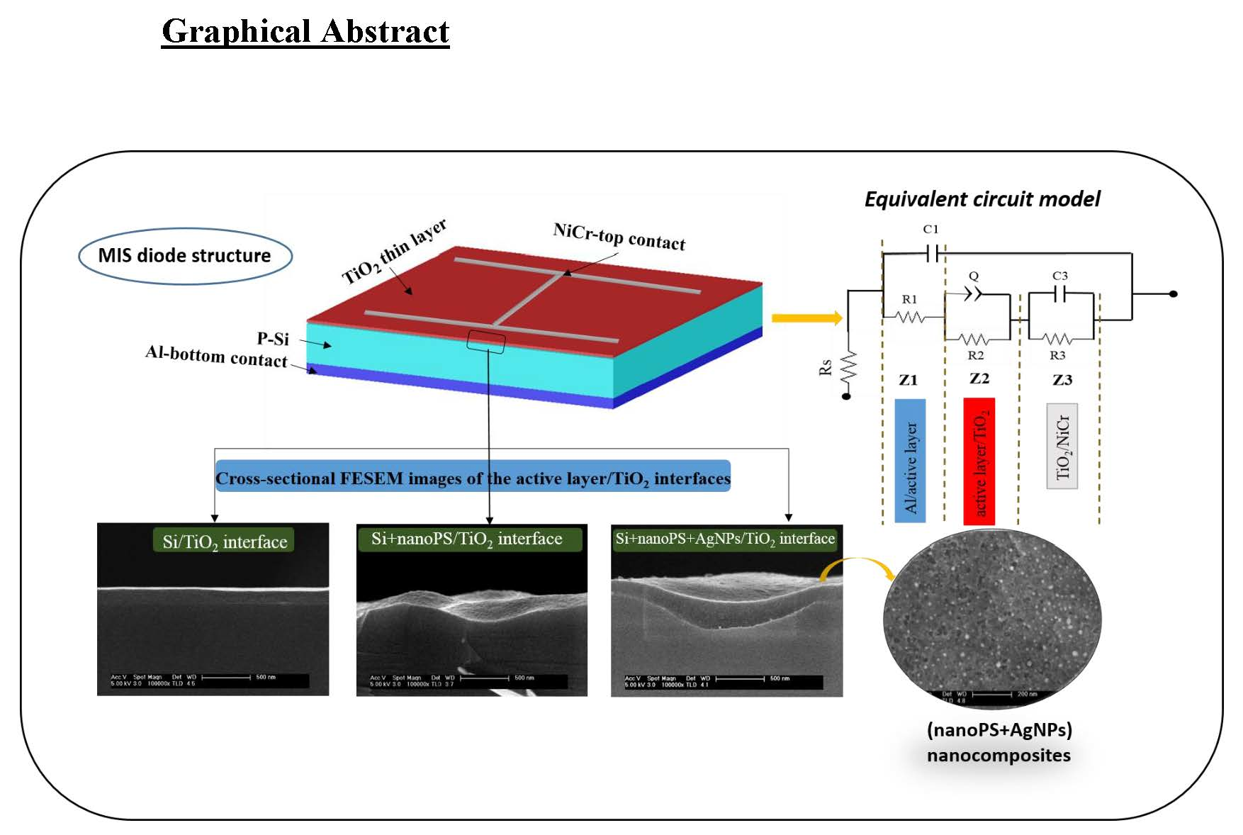
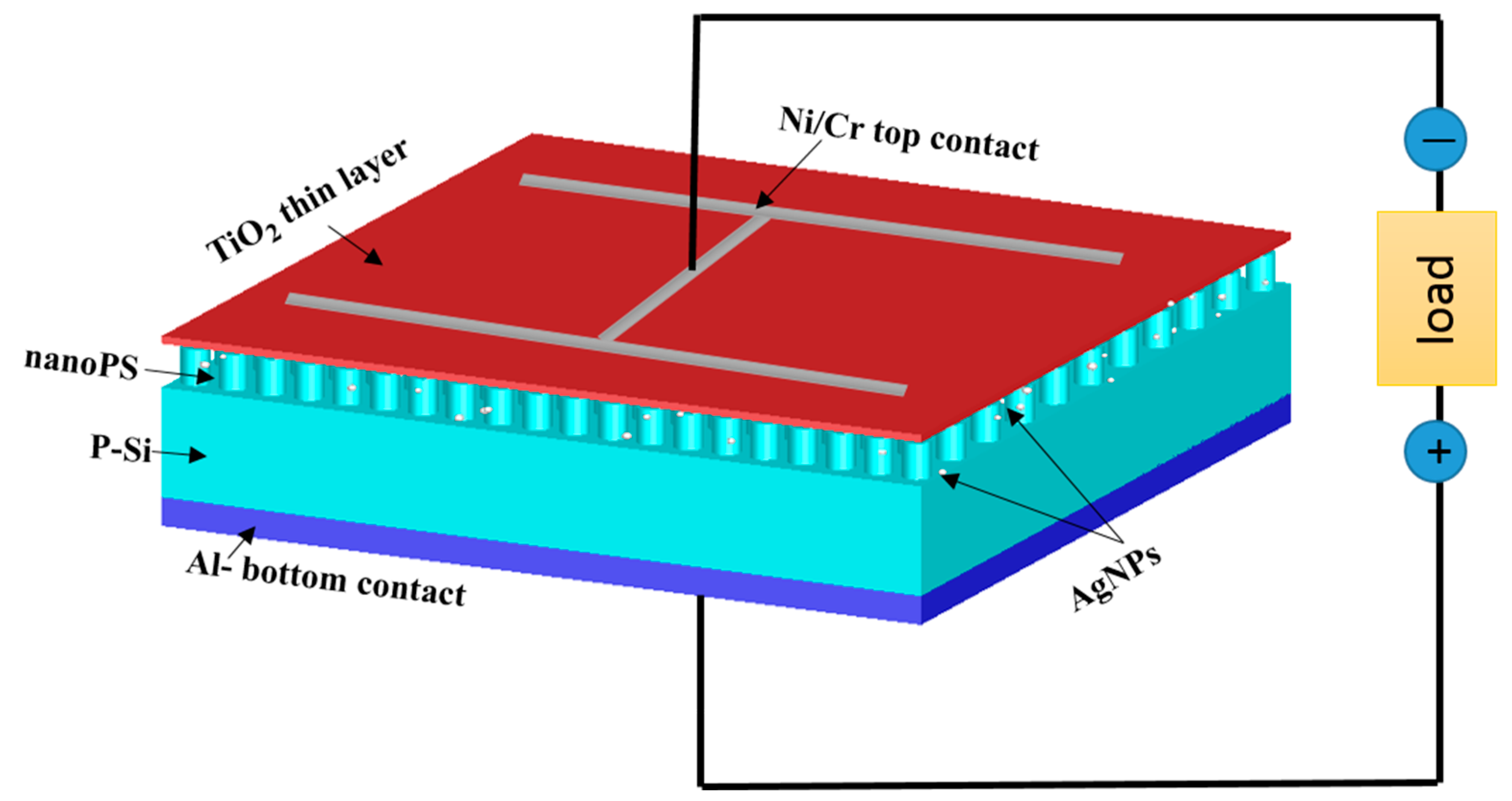
Figure 1. Schematic illustration of the structure of the Al/Si+nanoPS+AgNPs/TiO2/NiCr Schottky barrier diodes connected to a load. In this case, the active layer is Si+nanoPS+AgNPs.
Energies 13 02165 g001
Figure 2. (a) Cross-sectional, and (b) top views FESEMimages of a typical nanoPS+AgNPs layer (c), and (d) the same views upon deposition of a conformal TiO2 thin film.
Energies 13 02165 g002
Figure 3. Nyquist diagrams and impedance fittings corresponding to (a) Al/Si/TiO2/NiCr diodes, (b) Al/Si+nanoPS/TiO2/NiCr diodes, and (c) Al/Si+nanoPS+AgNPs/TiO2/NiCr diodes.
Energies 13 02165 g003
Figure 4. AC equivalent circuit model proposed to study the electrical behavior of the three Si-based MIS Schottky barrier diodes analyzed in this work. Depending on the particular diode, the active layer will be Si, Si+nanoPS, or Si+nanoPS+AgNPs.
Energies 13 02165 g004
Figure 5. Bode diagram to study the effect of frequency on the total impedance for the three MIS Schottky barrier devices analyzed.
Energies 13 02165 g005
Figure 6. Mott–Schottky diagram for the Al/Si/TiO2/NiCr Schottky junction device at 1, 5, and 10 kHz. The values calculated for Vfb and ND are shown in the inset.
Energies 13 02165 g006
Figure 7. Mott–Schottky diagram for the Al/Si+nanoPS/TiO2/NiCr Schottky junction device, at 1, 5, and 10 KHz. The values calculated for Vfb and ND are presented in the inset.
Energies 13 02165 g007
Figure 8. Mott–Schottky diagram for the Al/Si+nanoPS+AgNPs/TiO2/NiCr Schottky junction device, at 1, 5, and 10 kHz. The inset shows the values of Vfb and ND.
Energies 13 02165 g008
Figure 9. Current-voltage (I-V) curve for the three MIS Schottky junction devices under forward and reverse bias, showing in all cases a rectifying behavior. The inset portrays a typical I-V curve for Al/Si/NiCr devices (metal–semiconductor diodes), showing a notable increment in the values of current.
Energies 13 02165 g009
Figure 10. Experimental I-V data under forward bias and fittings to the modified ideal diode model used to extract the electrical parameters of the MIS Schottky barrier devices.
Energies 13 02165 g010
Table 1. Summary of the interfaces for the three Schottky junction diodes under analysis.
Schottky Diode Structure1st Interface2nd Interface3rd Interface
Al/Si/TiO2/NiCrAl/SiSi/TiO2TiO2/NiCr
Al/Si+nanoPS/TiO2/NiCrAl/Si+nanoPS Si+nanoPS/TiO2TiO2/NiCr
Al/Si+nanoPS+AgNPs/TiO2/NiCrAl/Si+nanoPS+AgNPsSi+nanoPS+AgNPs/TiO2TiO2/NiCr
Table 2. Comparison between the electrical RC elements for the three Si-based MIS Schottky barrier diodes studied in this work.
Calculated ParameterDevice Structure
Al/Si/TiO2/NiCrAl/Si+nanoPS/TiO2/NiCrAl/Si+nanoPS+AgNPs/TiO2/NiCr
Rs (Ω)1735123.2
C1 (nf)Al/active layer Interface5.72.315.5
R1 (kΩ)0.60.70.05
τ1 (µs) 3.421.610.77
Q (nS)Active layer/TiO2 Interface5416.821
a0.90.890.8
C2 (nf)4.010.910.04
R2 (kΩ)1.33.40.7
τ2 (µs)5.213.090.03
C3 (nf)TiO2/NiCr Interface19.731.513.2
R3 (kΩ)1.53.40.518
τ3 (µs)29.5597.655.52
Table 3. AC electrical parameters for the three structures determined from the Mott–Schottky plots at 1 KHz.
Device StructureVfb (V)Vbi (V)ND × 1015 (cm−3)
Al/Si/TiO2/NiCr−0.9−0.5150.617
Al/Si+ nanoPS/TiO2/NiCr−0.44−0.4650.121
Al/Si+nanoPS+AgNPs/TiO2/NiCr−0.09−0.1158.620
Table 4. DC electrical parameters obtained from the fitting of the experimental I-V curves.
Device StructureI0 (mA)nRs (kΩ)φB (V)
Al/Si/TiO2/NiCr2.32 × 10−72.123.210.87
Al/Si+nanoPS/TiO2/NiCr1.23 × 10−44.390.3630.72
Al/Si+nanoPS+AgNPs/TiO2/NiCr9.55 × 10−53.290.1390.73

