Article

Fabrication of Silicon Nanowire Metal-Oxide-Semiconductor Capacitors with Al2O3/TiO2/Al2O3 Stacked Dielectric Films for the Application to Energy Storage Devices

1
Department of Materials Process Engineering, Graduate School of Engineering, Nagoya University, Nagoya 464-8603, Japan
2
Department of Electrical and Mechanical Engineering, Graduate School of Engineering, Nagoya Institute of Technology, Nagoya 466-8555, Japan
*
Author to whom correspondence should be addressed.
Submission received: 3 June 2021 / Revised: 21 July 2021 / Accepted: 24 July 2021 / Published: 27 July 2021
(This article belongs to the Special Issue Advances in Devices for Energy Generation and Storage)

Abstract

:
Silicon nanowire (SiNW) metal-oxide-semiconductor (MOS) capacitors with Al2O3/TiO2/Al2O3 (ATA) stacked dielectric films were fabricated by metal-assisted chemical etching (MACE) and atomic layer deposition (ALD). High-angle annular dark field scanning transmission electron microscopy (HAADF-STEM) images revealed that SiNWs were conformally coated with ATA although the cross-sectional shapes of MACE-SiNWs were non-uniform and sharp spikes can be seen locally. The dielectric capacitance density of 5.9 μF/cm2 at V = −4 V of the perfect accumulation region was achieved due to the combination of the large surface area of the SiNW array and the high dielectric constant of ATA. The capacitance changed exponentially with the voltage at V < −4.3 V and the capacitance of 84 μF/cm2 was successfully achieved at V = −10 V. It was revealed that not only 3D structure and high-k material but also local nanostructure of SiNWs and stacked dielectric layers could contribute to the considerable high capacitance.

Graphical Abstract

1. Introduction

Electrostatic capacitors have attractive characteristics for the application in energy storage devices. Electrostatic capacitors have considerably higher power densities than batteries and electrochemical capacitors because of their short charge/discharge time (<1 μs) [1]. Moreover, electrostatic capacitors have high mechanical and thermal stabilities [1]. Since electrolyte solution is not necessary for electrostatic capacitors, there are much lower risks of fire and explosion compared to Li ion batteries and so on. However, electrostatic capacitors have the problem of considerably lower energy density than batteries and electrochemical capacitors. These characteristics limit the application to large-scale energy storage devices, for example, energy storage devices for renewable energies such as photovoltaic systems [2] and for vehicles [3,4]. In the case of capacitors, it is necessary to achieve high capacitance density for high energy density. Three-dimensional (3D) structuring is one of the methods to achieve high capacitance density. The capacitance density of an electrostatic capacitor with 3D structures with respect to its imprint area is given by the following equation.
C = ε r ε 0 S t A ,
Here, εr is the relative dielectric constant of the dielectric layer, ε0 is the permittivity of the vacuum, S is the electrode surface area, A is the top view area occupied by the device, and t is the dielectric layer thickness [5]. Thus, capacitors with 3D structures have high capacitance density because of the high S/A ratio.
There are several approaches to implement 3D structure into capacitors as summarized in Table 1. Banerjee et al. adopted anodic aluminum oxide (AAO) template to fabricate a 3D capacitor structure [6]. TiN/Al2O3/TiN stack layers were deposited on AAO templates with a pore depth of 10 μm and a pore diameter of 50 nm by atomic layer deposition (ALD). Further, 100 μF/cm2 was achieved by the metal/insulator/metal (MIM) capacitor. Silicon nanowires (SiNWs) are also one of the 3D structures with a considerably high S/A ratio. There are some reports of metal-oxide-semiconductor (MOS) capacitors using SiNWs. Morel et al. achieved the capacitance density of 18 μF/cm2 using SiNWs and 10-nm-thick-alumina (Al2O3) deposited by atomic layer deposition (ALD) as a dielectric material [7]. However, this method to prepare SiNWs needs a chemical vapor deposition (CVD) process using copper catalysts, which is a vacuum process and requires a high temperature (above ~400 °C) [7]. Moreover, it is difficult to control the length and diameter of SiNWs using this CVD process, which means less controllability on the capacitance density. We adopted a metal-assisted chemical etching method (MACE) [8,9,10] to fabricate SiNWs for a SiNW MOS capacitor. The MACE process is simple and SiNWs can be obtained at room temperature in a large area. The diameter of SiNWs prepared by MACE can be controlled using silica nanoparticles as etching masks [11]. If the length, diameter, dielectric film thickness, and dielectric material can be designed as intended, it is possible for higher capacitance density to be achieved with good controllability. A SiNW MOS capacitor has the potential of an easy fabrication process, good controllability, and higher capacitance density. A SiNW MOS capacitor with the SiNW length of 2.4 μm and Al2O3 thickness of 10 nm, fabricated by MACE achieved the maximum capacitance of 4.1 μF/cm2 [5]. However, there are no reports about a 3D MIM or MOS capacitor with a dielectric layer with a higher dielectric constant than Al2O3 as shown in Table 1. It is expected that a MOS capacitor with a high-k material and a 3D structure has a higher capacitance density. Titania (TiO2) is one of the high-k materials, which is easily prepared by ALD [12,13,14]. The relative dielectric constant of TiO2 ranges from 16 to 100 [13,15], which depends on the type of crystals. However, its relatively less narrow bandgap (~3.3 eV [16,17,18]) compared to other oxides causes high leakage current density. Thus, TiO2 combined with Al2O3 has been studied to overcome the problem. The preparation of Al2O3/TiO2/Al2O3 (ATA) [19,20,21], Al-doped TiO2 [20,22], (Al2O3)x(TiO2)y [23], nanolaminated Al2O3-TiO2 [24,25], and AlOx/TiOx/ZnOx [26] has been reported. Woo et al. fabricated flat MIM capacitors with ATA as an insulator and achieved 2.13 μF/cm2 at 1 MHz [19]. In this study, we implemented a SiNW template into a MOS capacitor with ATA as an insulator (Figure 1), and measured device characteristics. As a result, it was found that an increase of capacitance versus voltage and considerable high capacitance of 84 μF/cm2 at −10 V and 1 MHz can be achieved using SiNW MOS capacitors with ATA. It was revealed that not only 3D structure and high-k material but also the local nanostructure of SiNWs and stacked dielectric layers could contribute to the considerably high capacitance density.

2. Materials and Methods

p-type Czochralski-silicon (Si) (100) wafers, which have a 525 ± 25 μm thickness and resistivity of 2–5 Ω·cm, were used. SiNWs were prepared on the Si wafers by the MACE method. The Si wafers were dipped into the AgNO3 and HF mixed solution (AgNO3: HF: H2O = 120 mg: 10 mL: 40 mL) for 50 seconds to deposit Ag nanoparticles. After that, the Si wafers with the Ag nanoparticles were dipped into the H2O2 and HF mixed solution (H2O2: HF: H2O = 0.7 mL: 10 mL: 40 mL) to etch Si using the Ag nanoparticles as catalysts. The etching duration was set to 1.5 and 15 minutes, which corresponds to the SiNW length of 1 and 8 μm. The samples were immersed in HNO3 for 10 minutes and HF (5%) for 1 minute to remove Ag residues for three successive cycles. Before the dielectric thin film deposition on SiNWs, the samples were cleaned by dipping in a piranha solution at 120~140 °C for 15 minutes and an HF (5%) solution at room temperature for 1 minute. The stacked dielectric films of Al2O3(3.5 nm)/TiO2(16 nm)/Al2O3(3.5 nm) (ATA) were deposited on SiNWs and a flat Si substrate by ALD (Arradiance, GEMSTAR-6) at 200 °C. Al(CH3)3 (trimethyl-aluminum: TMA) and Ti(N(CH3)2)4 (tetrakis(dimethylamino)titanium: TDMAT) were used as precursors for Al2O3 and TiO2, respectively. H2O was also used as an oxidizer. The number of ALD cycles was set to make the total thickness of the ATA dielectric films ~23 nm. Al was deposited on surfaces covered with dielectric films by the vacuum evaporation method as surface electrodes. The size of the electrodes was 0.5 mmϕ. InGa was pasted on the back surface as a back electrode. The structure and dielectric film of the samples were characterized by scanning electron microscopy (SEM: JEOL, JSM-7001FA), energy dispersive X-ray spectrometry (EDS), Fourier transform infrared spectroscopy (FT-IR: Bruker, ALPHA), and high-angle annular dark field scanning transmission electron microscopy (HAADF-STEM: JEOL, JEM-ARM200F). Capacitance density and leakage current density characteristics were measured using an LCR meter (HP, 4248A) and an electrometer (Keithley, 6517B/J), respectively. The capacitance density was measured at the ac applied voltage of 10 mV and a frequency of 1 MHz.

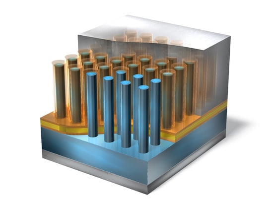
3. Results and Discussion

Figure 2a shows a cross-sectional scanning electron microscopy (SEM) image of an SiNW array of MACE for a duration of 15 minutes after ATA deposition. It was found that SiNWs were embedded in a dielectric material and the length of SiNWs is around 8 μm. The energy-dispersive X-ray spectroscopy (EDS) mappings of Al K, Ti K, and O K signals are shown in Figure 2b–d, respectively. From these EDS mappings, signals from Al, Ti, and O atoms were detected through the whole parts of the SiNWs. FT-IR spectra for ATA/SiNW samples with different lengths of SiNWs are shown in Figure S1. The FT-IR spectra showed two broad bands between 1000–700 cm−1 and 700–400 cm−1 and the absorbance of the broad bands was increased with increasing the length of SiNWs. According to the previous papers, the bands are attributed to vibrations characteristic of Al2O3 [32] and amorphous TiO2 [33,34]. If TiO2 was crystallized, a strong TiO2 anatase band at 435 cm−1 could be observed [14]. However, since there is no strong band at 435 cm−1, TiO2 is amorphous.
Figure 3 shows HAADF-STEM images of ATA/SiNWs cut into round slices. From Figure 3a, it was found that the SiNWs had random shapes, and each SiNW had relatively flat-face parts and sharp spikes. Regardless of such a non-uniform shape, the whole surface of SiNWs is successfully coated with ATA. This is because enough exposures of precursors were set as mentioned below. Figure 3b showed that the ATA film consisted of triple layers (Al2O3/TiO2/Al2O3). From the TEM image, each thickness of ATA was Al2O3(3.6 nm)/TiO2(15.2 nm)/Al2O3(3.7 nm). The ALD method provides uniform coatings inside holes and trenches with very high aspect ratios, using suitable pairs of reactants supplied in alternating doses of vapor [35]. In the experiment, the exposures of Al(CH3)3 (trimethyl-aluminum: TMA) and Ti(N(CH3)2)4 (tetrakis(dimethylamino)titanium: TDMAT), which are precursors for Al2O3 and TiO2, respectively, were set as 2.0 × 10⁵ and 4.4 × 10⁴ Langmuir (1 Langmuir = 1.33 × 10⁻⁴ Pa·s = 1.0 × 10⁻⁶ Torr·s), respectively. According to a kinetic model introduced by Gordon et al. [36], the exposure required to conformally coat a hole with a certain aspect ratio a is given by the depth of a hole/diameter of a hole.
( P t ) min = S C 2 π m k B T ( 1 + 19 4 a + 3 2 a 2 ) ,
In this equation, SC is the saturated coverage of the reactant molecule per unit surface area (molecules/m2), m (kg) is the mass of the reactant molecules, kB is the Boltzmann constant, and T (K) is the sample temperature. When the aspect ratio was assumed to be a = Depth ( 8 μ m ) / Diameter ( 0.1 μ m ) = 80 , the (Pt)min for TMA and TDMAT were estimated to be 2.8 × 10⁴ and 1.4 × 10⁴ Langmuir, respectively. The exposures used in this experiment are large enough compared to the (Pt)min. Therefore, conformally coated SiNWs were successfully obtained. The cross-sectional SEM images of ATA/SiNWs after Al deposition are shown in Figure S2. It was found that ATA/SiNWs were not perfectly covered with Al. Al electrodes were localized on the surface from the top to the middle of SiNWs. To charge electrons fully in the SiNW MOS capacitor, the perfectly covered Al electrode is preferable. Therefore, it is possible to enhance the capacitance density further by improving the coverage of Al electrodes. The length of SiNWs can be controlled by the duration of MACE. To increase the surface area of the SiNW array, longer SiNW is preferable. However, Al flakes can be found only until the middle of SiNWs. Therefore, in this study, 1 and 8 μm were adopted for the lengths of SiNWs.
Figure 4a shows capacitance-voltage (C-V) characteristics of MOS capacitors using a flat Si and a SiNW with L = 1 and 8 μm. The C-V curve of the flat capacitor has typical MOS characteristics. Assuming that there are few fixed charges in the ATA film in the flat MOS capacitor, the flat band voltage (VFB) of −0.87 V should be obtained, which comes from the work function difference between Al and Si (ϕMS = 0.87 eV [37]). However, the VFB from Figure 4a was estimated to be −2.05 V, suggesting that there are fixed charges in the ATA film. The fixed charge density (Qf) can be calculated by the following equation,
Q f = C o x q A ( ϕ MS + V FB ) ,
where Cox is the measured dielectric capacitance at accumulation, q is the elementary charge, and A is the area of electrodes. The positive fixed charge density of the flat MOS capacitor was calculated to be 5.1 × 1012 cm−2. These positive fixed charges seem to mainly come from dipoles induced by cation intermixing near the TiO2/Al2O3 interface [38]. Zhang et al. reported that local intermixing of TiO2 and Al2O3 in the annealed dielectric is suggested by the grading of the composition profile over a distance of ∼1 nm with respect to the nominal interface positions. When titanium atoms are incorporated in aluminum sites in Al2O3, they act as electron donors (TiAl+), whereas Al in TiO2 are expected to be incorporated as acceptors occupying the Ti site (AlTi). Many of the TiAl species in Al2O3 are expected to be in a positive charge state, whereas the AlTi defects in TiO2 are predicted to occur in the negative charge state. That is why dipoles are generated near the TiO2/Al2O3 interfaces. Since the thickness of Al2O3 is very thin, with a value of 3.6 nm, the positive charges influence the depletion layer in p-type Si, and the flat band voltage was shifted.
At the inversion region (V = 1 V), the depletion layer capacities (Cd) of flat and SiNW MOS capacitors are 2.8 × 10⁻² and 2.7 × 10⁻² μF/cm2, respectively. On the other hand, in the accumulation region (V < VFB), Cd disappears and only Cox can be measured shown in Figure S3. The capacitance density at the accumulation region (V = −5 V) of 0.7 μF/cm2 was achieved by the flat MOS capacitor using ATA. In the case of the SiNW MOS capacitor, two regions with a gradual slope can be seen in both L = 1 and 8 μm. This suggests that there are two kinds of parts with and without dipoles in ATA. In the case of L = 8 μm, region 1 in the range of −1 V < V < −0.5 V represents the capacitance derived from the accumulation in the part without any dipoles, which means few fixed charges exist in an insulator. In fact, the VFB = −0.25 V at the part without any dipoles is much less than VFB = −2.05 V of the flat MOS capacitor with dipoles. On the other hand, region 2 in the range of −4 V < V < −3.5 V represents the capacitance derived from the accumulation in the part with the dipoles. The flat band voltage of the second region is around −1.9 V, which is comparable to VFB = −2.05 V of the flat MOS capacitor. The capacitance in the range of −4 V < V < −3.5 V is a plateau, suggesting that charging was completely finished in all the parts with and without dipoles. The capacitance densities of SiNW MOS capacitors with 1 and 8 μm were 3.2 and 5.9 μF/cm2 at −4 V. In this range, it can be regarded as a perfect accumulation region and this capacitance value was 4.6 and 8.4 times higher than that of the flat MOS capacitor using ATA, respectively. This is the effect of the 3D template. The higher capacitance density mainly comes from the larger surface area of a SiNW array than the flat Si substrate. In the case of a single Al2O3 with a thickness of 25 nm, as shown in Figure S4, the capacitance densities of flat and SiNW MOS capacitors with L = 1 μm were 0.31 and 0.55 μF/cm2, respectively. Therefore, by inserting a TiO2 layer, capacitance densities of flat and SiNW MOS capacitors were 2.3 and 5.8 times enhanced, respectively. It suggests that the SiNW structure and ATA causes the capacitance density to be enhanced synergistically. The dielectric constant of a single Al2O3 and ATA is estimated at 8.8 and 19.8, respectively. Therefore, by inserting a TiO2 layer, the dielectric constant was enhanced 2.25 times. In the case of a single TiO2 layer, the C-V measurement was not successful due to a too-large leakage current.
The parts without dipoles are attributed to the shape of SiNWs. As shown in the HAADF-STEM images of Figure 3a, several sharp spikes can be seen. At the sharp spikes, two different TiO2/Al2O3 interfaces are close and intersect each other. That is why the cancellation of dipoles was caused. The dependence of the capacitance on the voltage can be observed at V < −4.3 V even though the depletion region seems to perfectly disappear (Region 3). Such a dependence is often observed on some capacitors using high-k films. The detailed investigation is written below.
Figure 4b shows the leakage current density-voltage (J-V) of the flat and SiNW MOS capacitors using ATA. The vertical axis shows the absolute value of leakage current density. The SiNW MOS capacitor shows a higher leakage current density than the flat MOS capacitor in the whole applied voltage. One possible reason is the area used in this calculation. The leakage current density was obtained by dividing the measured leakage current by a top view area of the device, indicating that the leakage current density of SiNW MOS capacitors is overestimated. Ideally, the increasing rates of capacitance density and leakage current density by implementing a 3D structure should be equal. However, the increasing rate of capacitance density was 8.4 times. On the other hand, the leakage current density of the SiNW MOS capacitor at the accumulation region is almost 104 times higher than that of the flat MOS capacitor. Therefore, other effects should be considered. The Al2O3 layers in the ATA are not sufficiently thick to prevent tunneling current. Under the application of a high electric field, the barrier of Al2O3 has a triangular shape. Tunneling through the triangular barrier can be characterized as Fowler–Nordheim (F-N) tunneling [39]. The F-N current density is given by the following equation.
J E 2 exp [ 4 2 m e ( q ϕ o x ) 3 / 2 3 q E ] ,
Here, E is the net electric field applied to a barrier oxide layer, me is an effective mass in a barrier material, q is an elementary charge, ϕox is a barrier height, and ħ is a Dirac constant. Since under high voltage biases, the barrier thickness is reduced, the tunneling current density was increased according to Equation (4). The dashed line in Figure 4c shows fitted curves. me = 0.2m0 was used as an effective mass in Al2O3 [40]. Assuming that E = V/dox can be applied and dox = 3.7 nm, the barrier heights (ox) are estimated at 0.36 and 1.1 eV, respectively. These values are lower than the conduction band offset between TiO2 and Al2O3. The details are discussed in the last paragraph. The leakage current density of the SiNW MOS capacitor with L = 1 μm is larger than that of L = 8 μm. This is due to the difference of the existence of the non-coverage area of an Al electrode.
Schmitz et al. reported the RF capacitance-voltage characterization of MOSFETs with high leakage dielectrics [41]. This can be understood conceptually by considering a simple three-element equivalent circuit for the leaky MOS capacitor as shown in Figure S5. The capacitance C is connected in parallel with a differential conductance g derived from the leakage current. R is an external resistance. A capacitance measurement is only straightforward when the capacitance is large enough (typically at least 1 pF), and the quality factor (Qf) is larger than unity. To obtain the Qf > 1, the minimum measurement frequency can be expressed as
f min = 1 1 4 g R ( 1 + g R ) 4 π R C g 2 π C ,
From a linear fitting in the range of −4 to −1 V in Figure 4b, conductance in the SiNW MOS capacitor with the length of 8 μm is estimated roughly at 3.3 mS. For a S = π(0.025)2 cm2 MOS capacitor, typical values are C = 5.9 μF/cm2 × S = 12 nF, g = 3.3 mS, and R = 10 Ω leading to fmin = 49 kHz. We tried to conduct C-V measurement at 50 kHz as shown in Figure S6. The capacitance density was decreased by increasing the absolute value of the applied voltage due to the tunnel leakage current [42]. Since we conducted the C-V measurement at 1 MHz, the influence of the leakage current on the C-V measurement can be ignored in this measurement.
To conduct a more detailed investigation of capacitance characteristics at V < −4.3 V (Region 3) of the SiNW MOS capacitor using ATA, the C-V characteristics in the range of −10 V < V < −4 V was measured as shown in Figure 5. The exponential increase with decreasing voltage can be observed at V < −6 V. The considerable high capacitance density of 84 μF/cm2 can be obtained at V = −10 V. The combination of the local nanostructure in SiNWs and the interface of the stacked dielectric layers could contribute to a capacitance density 120 times higher compared to the flat capacitor with ATA.
To understand this behavior, an equivalent circuit of the MOS capacitor with ATA was assumed as shown in Figure 6a. Not only Cox but also the capacitance element at the interface of TiO2/Al2O3 (Ci) was considered. The total impedance observed was measured as an equivalent-series RC combination as indicated in Figure 6b in this experiment. By equating the circuits (a) and (b), it can be shown that
R = R i + R o x 1 + ω 2 R o x 2 C i 2 ,
1 ω C = 1 ω C i + ω R o x 2 C o x 1 + ω 2 R o x 2 C o x 2 ,
From Equation (7), the total capacitance density can be represented as
C = C i ( 1 + ω 2 R o x 2 C o x 2 ) 1 + ω 2 ( R o x 2 C o x C i + R o x 2 C o x 2 ) ,
When Ci is much larger than Cox and ω 2 R o x 2 C o x C i 1 , Equation (9) can be obtained.
C C o x + 1 ω 2 R o x 2 C o x ,
Figure 7 shows the capacitance–frequency characteristics of the SiNW MOS capacitor with ATA (L = 8 μm) at V = −5 V. From Equation (8), Cox = 5.0 μF/cm2, Ci = 3.9 × 10³ μF/cm2, and Rox = 4.1 × 10⁻⁷ MΩ·cm2 were obtained. Ci is much larger than Cox. In general, the capacitance density of an electric double layer is ~20 μF/cm2. If the length, diameter, and filling ratio are 8 μm, 100 nm, and 0.5, the surface area is about 160 times compared with a flat substrate. If such an electric double layer exists at the interface in the ATA, 3.9 × 10³ μF/cm2 can be realized. From the Rox value, gox = 4.8 mS can be obtained, which is comparable with that of 3.3 mS from Figure 4c. Assuming that the electric field is uniform at E = V/dox and Rox is determined by Equation (4), the relationship between C and V can be obtained as follows.
C V 2 exp ( 8 2 m e ( q ϕ o x ) 3 / 2 d o x 3 q ( V ) ) + C o x ,
By fitting Equation (10) and the C-V characteristics as shown in Figure 5, ox = 1.1 eV was obtained. This value corresponds to that obtained from Figure 4c. To discuss the height of the barrier for tunneling, the calculated MOS band diagram at V = −5 V is shown in Figure 8. These simulation results were obtained using the TCAD software Silvaco Atlas. Since, under a large bias, the voltage high electric field is applied to the Al2O3 layer on the p-type Si side, the barrier of Al2O3 has a triangular shape. Therefore, F-N tunneling occurs at the interface. The holes are supplied from the p-type Si into the interface between TiO2/Al2O3 on the metal side. It is believed that this is the origin of the Ci. In this case, the hole barrier height at the Al2O3/p-type Si interface is 2.37 eV, which is larger than the obtained value of 1.1 eV. One possibility is the non-uniform electric field distribution. In this calculation of the barrier height, a uniform electric field of E = V/dox was assumed. However, at local sharp spikes of SiNWs seen in Figure 3a, the electric field is concentrated, leading to high leakage current according to Equation (4). Therefore, ox was underestimated. Another reason for the lower barrier height is defects in Al2O3. As mentioned before, cation intermixing forms positive and negative charge states in Al2O3 [38]. The positive charge states are located at a higher level by 3.5 eV from the top of the valence band in Al2O3. It is possible that positive charge states assist hole tunneling, leading to the underestimation of the barrier height.
If this model is true, the interface charging phenomenon at TiO2/Al2O3 is very important. Since this charging can be obtained under a DC bias, it is acceptable to charge electricity from renewable energy. It should be studied further. Apparently, from Figure 5, the capacitance density seems to increase until Ci by increasing the absolute value of the applied voltage. However, if the leakage at the TiO2/Al2O3 interface on the metal side becomes remarkable due to tunneling, the capacitance density could be decreased. To realize a high capacitance density close to Ci, further investigation including device design is necessary.

4. Conclusions

SiNW MOS capacitors with ATA stacked dielectric films were fabricated by MACE and ALD. HAADF-STEM images revealed that although the cross-sectional shapes of MACE-SiNWs are non-uniform and sharp spikes can be seen locally, SiNWs were conformally coated with ATA. Each thickness of ATA was Al2O3(3.6 nm)/TiO2(15.2 nm)/Al2O3(3.7 nm). The dielectric capacitance density of 5.9 μF/cm2 at V = − 4 V of the perfect accumulation region was achieved due to the combination of the large surface area of the SiNW array and the high dielectric constant of ATA. The capacitance changed exponentially with voltage at V < −4.3 V and the maximum capacitance of 84 μF/cm2 was successfully achieved at V = −10 V. Not only 3D structure and high-k dielectrics, but also the combination of local nanostructure in SiNWs and the interface of the stacked dielectric layers, could contribute to a capacitance density 120 times higher compared to the flat capacitor with ATA. It was found that ATA/SiNWs were not perfectly covered with the Al electrode. Therefore, it is possible to enhance the capacitance density further by improving the coverage of the Al electrodes.

Supplementary Materials

The following are available online at https://0-www-mdpi-com.brum.beds.ac.uk/article/10.3390/en14154538/s1, Figure S1: FT-IR spectra of SiNW arrays and a flat Si wafer coated by ATA. Two pronounced bands are attributed to IR absorption by Si–O2 complexes (at ~1107 cm−1) and by Si lattice phonons (at ∼610 cm−1), respectively. An Al2O3 broad band (500~1000 cm−1) can be seen. If TiO2 was crystallized, strong TiO2 anatase band at 435 cm−1 could be observed. However, since there is no strong band at 435 cm−1, TiO2 is amorphous, Figure S2. Cross-sectional SEM image of a SiNW MOS capacitor after Al evaporation. Flakes of Al crystals can be seen from the top to middle of SiNWs. Since Al electrodes were deposited by thermal evaporation, SiNWs were not perfectly coated with Al, Figure S3. Energy band diagram and equivalent circuit of a MOS capacitor in the range of V < 0, Figure S4. C-V characteristics of (Dashed line) a flat MOS capacitor and (Solid line) a SiNW MOS capacitor using 25-nm-thick Al2O3 as an insulator. The length of SiNWs is 1.0 μm, Figure S5. Equivalent circuit approximation of a leaky MOS capacitor, Figure S6. C-V characteristics of the SiNW MOS capacitor with the length of 8 μm measured at 50 kHz.

Author Contributions

Conceptualization, Y.K.; methodology, S.K., N.U. and Y.K.; validation, K.G., S.K., S.M., N.U. and Y.K.; formal analysis, R.N.; investigation, R.N.; resources, N.U. and Y.K.; data curation, Y.K.; writing—original draft preparation, R.N.; writing—review and editing, K.G., S.K., S.M., N.U. and Y.K.; visualization, R.N. and Y.K.; supervision, N.U. and Y.K.; project administration, Y.K.; funding acquisition, Y.K. All authors have read and agreed to the published version of the manuscript.

Funding

This research was funded by Japan Society for the Promotion of Science, Grant-in-Aid for Scientific Research (KAKENHI), grant number 16K14546.

Institutional Review Board Statement

Not applicable.

Informed Consent Statement

Not applicable.

Data Availability Statement

Not applicable.

Acknowledgments

This work was supported in part by Japan Society for the Promotion of Science Grant-in-Aid for Scientific Research (KAKENHI, No. 16K14546).

Conflicts of Interest

The authors declare no conflict of interest.

References

  1. Zhang, L.; Liu, M.; Ren, W.; Zhou, Z.; Dong, G.; Zhang, Y.; Peng, B.; Hao, X.; Wang, C.; Jiang, Z.-D.; et al. ALD preparation of high-k HfO2 thin films with enhanced energy density and efficient electrostatic energy storage. RSC Adv. 2017, 7, 8388–8393. [Google Scholar] [CrossRef] [Green Version]
  2. Chen, C.; Duan, S.; Cai, T.; Liu, B.; Hu, G. Smart energy management system for optimal microgrid economic operation. In IET Renewable Power Generation; Institution of Engineering and Technology: Stevenage, UK, 2011; Volume 5, pp. 258–267. [Google Scholar]
  3. Lam, L.T.; Louey, R. Development of ultra-battery for hybrid-electric vehicle applications. J. Power Sources 2006, 158, 1140–1148. [Google Scholar] [CrossRef]
  4. Wagner, F.T.; Lakshmanan, B.; Mathias, M.F. Electrochemistry and the Future of the Automobile. J. Phys. Chem. Lett. 2010, 1, 2204–2219. [Google Scholar] [CrossRef]
  5. Leontis, I.; Botzakaki, M.A.; Georga, S.N.; Nassiopoulou, A.G. High capacitance density MIS capacitor using Si nanowires by MACE and ALD alumina dielectric. J. Appl. Phys. 2016, 119, 244508. [Google Scholar] [CrossRef]
  6. Banerjee, P.; Perez, I.; Henn-Lecordier, L.; Lee, S.B.; Rubloff, G.W. Nanotubular metal–insulator–metal capacitor arrays for energy storage. Nat. Nanotechnol. 2009, 4, 292–296. [Google Scholar] [CrossRef] [PubMed]
  7. Morel, P.H.; Haberfehlner, G.; Lafond, D.; Audoit, G.; Jousseaume, V.; Leroux, C.; Fayolle-Lecocq, M.; Baron, T.; Ernst, T. Ultra high density three dimensional capacitors based on Si nanowires array grown on a metal layer. Appl. Phys. Lett. 2012, 101, 083110. [Google Scholar] [CrossRef]
  8. Zhang, M.L.; Peng, K.Q.; Fan, X.; Jie, J.S.; Zhang, R.Q.; Lee, S.T.; Wong, N.B. Preparation of large-area uniform silicon nanowires arrays through metal-assisted chemical etching. J. Phys. Chem. C 2008, 112, 4444–4450. [Google Scholar] [CrossRef]
  9. Chartier, C.; Bastide, S.; Lévy-Clément, C. Metal-assisted chemical etching of silicon in HF–H2O2. Electrochim. Acta 2008, 53, 5509–5516. [Google Scholar] [CrossRef]
  10. Nassiopoulou, A.G.; Gianneta, V.; Katsogridakis, C. Si nanowires by a single-step metal-assisted chemical etching process on lithographically defined areas: Formation kinetics. Nanoscale Res. Lett. 2011, 6, 597. [Google Scholar] [CrossRef] [Green Version]
  11. Kato, S.; Watanabe, Y.; Kurokawa, Y.; Yamada, A.; Ohta, Y.; Niwa, Y.; Hirota, M. Metal-Assisted Chemical Etching Using Silica Nanoparticle for the Fabrication of a Silicon Nanowire Array. Jpn. J. Appl. Phys. 2012, 51, 02BP09. [Google Scholar] [CrossRef]
  12. Xie, Q.; Jiang, Y.-L.; Detavernier, C.; Deduytsche, D.; Meirhaeghe, R.L.V.; Ru, G.-P.; Li, B.-Z.; Qu, X.-P. Atomic layer deposition of TiO2 from tetrakis-dimethyl-amido titanium or Ti isopropoxide precursors and H2O. J. Appl. Phys. 2007, 102, 083521. [Google Scholar] [CrossRef]
  13. Dang, V.-S.; Parala, H.; Kim, J.H.; Xu, K.; Srinivasan, N.B.; Edengeiser, E.; Havenith, M.; Wieck, A.D.; de los Arcos, T.; Fischer, R.A.; et al. Electrical and optical properties of TiO2 thin films prepared by plasma-enhanced atomic layer deposition. Phys. Status Solidi (a) 2014, 211, 416–424. [Google Scholar] [CrossRef]
  14. Dueñas, S.; Castán, H.; García, H.; Andrés, E.S.; Toledano-Luque, M.; Mártil, I.; González-Díaz, G.; Kukli, K.; Uustare, T.; Aarik, J. A comparative study of the electrical properties of TiO2films grown by high-pressure reactive sputtering and atomic layer deposition. Semicond. Sci. Technol. 2005, 20, 1044–1051. [Google Scholar] [CrossRef]
  15. Alexandrov, P.; Koprinarova, J.; Todorov, D. Dielectric properties of TiO2-films reactively sputtered from Ti in an RF magnetron. Vacuum 1996, 47, 1333–1336. [Google Scholar] [CrossRef]
  16. Aarik, J.; Aidla, A.; Kiisler, A.-A.; Uustare, T.; Sammelselg, V. Effect of crystal structure on optical properties of TiO2 films grown by atomic layer deposition. Thin Solid Films 1997, 305, 270–273. [Google Scholar] [CrossRef]
  17. Avasthi, S.; McClain, W.E.; Man, G.; Kahn, A.; Schwartz, J.; Sturm, J.C. Hole-blocking titanium-oxide/silicon heterojunction and its application to photovoltaics. Appl. Phys. Lett. 2013, 102, 203901. [Google Scholar] [CrossRef] [Green Version]
  18. Mochizuki, T.; Gotoh, K.; Ohta, A.; Ogura, S.; Kurokawa, Y.; Miyazaki, S.; Fukutani, K.; Usami, N. Activation mechanism of TiOx passivating layer on crystalline Si. Appl. Phys. Express 2018, 11, 102301. [Google Scholar] [CrossRef]
  19. Woo, J.-C.; Chun, Y.-S.; Joo, Y.-H.; Kim, C.-I. Low leakage current in metal-insulator-metal capacitors of structural Al2O3/TiO2/Al2O3 dielectrics. Appl. Phys. Lett. 2012, 100, 081101. [Google Scholar] [CrossRef]
  20. Lehnert, W.; Ruhl, G.; Gschwandtner, A. Plasma enhanced atomic layer batch processing of aluminum doped titanium dioxide. J. Vac. Sci. Technol. A 2012, 30, 01A152. [Google Scholar] [CrossRef]
  21. Padhi, P.S.; Ajimsha, R.S.; Chetia, S.K.; Das, A.K.; Sahu, V.K.; Misra, P. Reduced leakage current in Al2O3/TiO2/Al2O3 dielectric stacks grown by pulsed laser deposition. AIP Conf. Proc. 2020, 2265, 030190. [Google Scholar]
  22. Kim, S.K.; Choi, G.-J.; Lee, S.Y.; Seo, M.; Lee, S.W.; Han, J.H.; Ahn, H.-S.; Han, S.; Hwang, C.S. Al-Doped TiO2 Films with Ultralow Leakage Currents for Next Generation DRAM Capacitors. Adv. Mater. 2008, 20, 1429–1435. [Google Scholar] [CrossRef]
  23. Shi, L.; Yin, J.; Yin, K.; Gao, F.; Xia, Y.; Liu, Z. An investigation into ultra-thin pseudobinary oxide (TiO2)x(Al2O3)1-x films as high-k gate dielectrics. Appl. Phys. A 2008, 90, 379–384. [Google Scholar] [CrossRef]
  24. Kim, Y.S.; Yun, S.J. Nanolaminated Al2O3–TiO2 thin films grown by atomic layer deposition. J. Cryst. Growth 2005, 274, 585–593. [Google Scholar] [CrossRef]
  25. Jeon, W.; Chung, H.-S.; Joo, D.; Kang, S.-W. TiO2/Al2O3/TiO2 Nanolaminated Thin Films for DRAM Capacitor Deposited by Plasma-Enhanced Atomic Layer Deposition. Electrochem. Solid-State Lett. 2008, 11, H19. [Google Scholar] [CrossRef]
  26. Lei, J.; Fang, C.; Liu, C.; Wu, D.; Li, A.-D. Flexible Al-Ti-Zn-O MIM capacitors fabricated by room temperature atomic layer deposition and their electrical performances. J. Alloys Compd. 2021, 870, 159391. [Google Scholar] [CrossRef]
  27. Lin, B.-C.; Ku, C.-S.; Lee, H.-Y.; Chakroborty, S.; Wu, A.T. Analysis of arrayed nanocapacitor formed on nanorods by flow-rate interruption atomic layer deposition. Appl. Surf. Sci. 2017, 426, 224–228. [Google Scholar] [CrossRef]
  28. Kemell, M.; Ritala, M.; Leskelä, M.; Ossei-Wusu, E.; Carstensen, J.; Föll, H. Si/Al2O3/ZnO:Al capacitor arrays formed in electrochemically etched porous Si by atomic layer deposition. Microelectron. Eng. 2007, 84, 313–318. [Google Scholar] [CrossRef]
  29. Burke, M.; Blake, A.; Djara, V.; O’Connell, D.; Povey, I.M.; Cherkaoui, K.; Monaghan, S.; Scully, J.; Murphy, R.; Hurley, P.K.; et al. High aspect ratio iridescent three-dimensional metal–insulator–metal capacitors using atomic layer deposition. J. Vac. Sci. Technol. A 2015, 33, 01A103. [Google Scholar] [CrossRef]
  30. Zhang, G.; Wu, H.; Chen, C.; Wang, T.; Wu, W.; Yue, J.; Liu, C. Transparent Nanotubular Capacitors Based On Transplanted Anodic Aluminum Oxide Templates. ACS Appl. Mater. Interfaces 2015, 7, 5522–5527. [Google Scholar] [CrossRef]
  31. Haspert, L.C.; Lee, S.B.; Rubloff, G.W. Nanoengineering Strategies for Metal–Insulator–Metal Electrostatic Nanocapacitors. ACS Nano 2012, 6, 3528–3536. [Google Scholar] [CrossRef]
  32. Ferguson, J.D.; Weimer, A.W.; George, S.M. Atomic Layer Deposition of Al2O3 Films on Polyethylene Particles. Chem. Mater. 2004, 16, 5602–5609. [Google Scholar] [CrossRef]
  33. Trasferetti, B.C.; Davanzo, C.U.; Zoppi, R.A.; da Cruz, N.C.; de Moraes, M.A.B. Berreman effect applied to phase characterization of thin films supported on metallic substrates: The case of TiO2. Phys. Rev. B 2001, 64, 125404. [Google Scholar] [CrossRef] [Green Version]
  34. Jõgi, I.; Pärs, M.; Aarik, J.; Aidla, A.; Laan, M.; Sundqvist, J.; Oberbeck, L.; Heitmann, J.; Kukli, K. Conformity and structure of titanium oxide films grown by atomic layer deposition on silicon substrates. Thin Solid Films 2008, 516, 4855–4862. [Google Scholar] [CrossRef]
  35. Hausmann, D.M.; Kim, E.; Becker, J.; Gordon, R.G. Atomic Layer Deposition of Hafnium and Zirconium Oxides Using Metal Amide Precursors. Chem. Mater. 2002, 14, 4350–4358. [Google Scholar] [CrossRef]
  36. Gordon, R.G.; Hausmann, D.; Kim, E.; Shepard, J. A Kinetic Model for Step Coverage by Atomic Layer Deposition in Narrow Holes or Trenches. Chem. Vap. Depos. 2003, 9, 73–78. [Google Scholar] [CrossRef]
  37. Ren, Y.; Nursam, N.M.; Wang, D.; Weber, K.J. Charge stability in LPCVD silicon nitride for surface passivation of silicon solar cells. In Proceedings of the 2010 35th IEEE Photovoltaic Specialists Conference, Honolulu, HI, USA, 20–25 June 2010; pp. 000897–000901. [Google Scholar]
  38. Zhang, L.; Janotti, A.; Meng, A.C.; Tang, K.; Van de Walle, C.G.; McIntyre, P.C. Interfacial Cation-Defect Charge Dipoles in Stacked TiO2/Al2O3 Gate Dielectrics. ACS Appl. Mater. Interfaces 2018, 10, 5140–5146. [Google Scholar] [CrossRef] [PubMed]
  39. Lenzlinger, M.; Snow, E.H. Fowler—Nordheim Tunneling into Thermally Grown SiO2. J. Appl. Phys. 1969, 40, 278–283. [Google Scholar] [CrossRef]
  40. Padovani, A.; Larcher, L.; Marca, V.D.; Pavan, P.; Park, H.; Bersuker, G. Charge trapping in alumina and its impact on the operation of metal-alumina-nitride-oxide-silicon memories: Experiments and simulations. J. Appl. Phys. 2011, 110, 014505. [Google Scholar] [CrossRef]
  41. Schmitz, J.; Cubaynes, F.N.; Havens, R.J.; De Kort, R.; Scholten, A.J.; Tiemeijer, L.F. RF capacitance-voltage characterization of MOSFETs with high leakage dielectrics. IEEE Electron Device Lett. 2003, 24, 37–39. [Google Scholar] [CrossRef] [Green Version]
  42. Choi, C.-H.; Goo, J.-S.; Oh, T.-Y.; Yu, Z.; Dutton, R.W.; Bayoumi, A.; Min, C.; Voorde, P.V.; Vook, D.; Diaz, C.H. MOS C-V characterization of ultrathin gate oxide thickness (1.3–1.8 nm). IEEE Electron Device Lett. 1999, 20, 292–294. [Google Scholar] [CrossRef]
  43. Alimardani, N.; King, S.W.; French, B.L.; Tan, C.; Lampert, B.P.; Conley, J.F., Jr. Investigation of the impact of insulator material on the performance of dissimilar electrode metal-insulator-metal diodes. J. Appl. Phys. 2014, 116, 024508. [Google Scholar] [CrossRef] [Green Version]
  44. Yang, X.; Zheng, P.; Bi, Q.; Weber, K. Silicon heterojunction solar cells with electron selective TiOx contact. Sol. Energy Mater. Sol. Cells 2016, 150, 32–38. [Google Scholar] [CrossRef]
  45. Sankapal, B.R.; Lux-Steiner, M.C.; Ennaoui, A. Synthesis and characterization of anatase-TiO2 thin films. Appl. Surf. Sci. 2005, 239, 165–170. [Google Scholar] [CrossRef]
Figure 1. Schematic diagram of a fabricated SiNW MOS capacitor. The insulator consists of an Al2O3(3.6 nm)/TiO2(15.2 nm)/Al2O3(3.7 nm) stacked structure.
Energies 14 04538 g001
Figure 2. (a) Cross-sectional SEM image of a SiNW array coated with ATA. The SiNW array was prepared by MACE for 15 min. The length of SiNWs is 8 μm, (b) EDS mappings of Si K, (c) Al K, (d) Ti K signal.
Energies 14 04538 g002
Figure 3. Round-sliced HAADF-STEM images of a SiNW array coated with ATA, (a) × 160,000, (b) × 1,600,000. Each thickness of ATA was Al2O3(3.6 nm)/TiO2(15.2 nm)/Al2O3(3.7 nm).
Energies 14 04538 g003
Figure 4. (a) C-V characteristics, (b) J-V characteristics of SiNW MOS capacitors (blue and red solid line) and flat MOS capacitors (black solid line). The vertical axis shows the absolute value of leakage current density. (c) J-V characteristics of SiNW MOS capacitors fitted by the Fowler–Nordheim tunneling equation.
Energies 14 04538 g004
Figure 5. C-V characteristics of the SiNW MOS capacitor using ATA (L = 8 μm) in the high voltage region (−10 V < V< −4 V). The solid line shows an experimental curve, and the dashed line shows theoretical capacitance density represented by (10).
Energies 14 04538 g005
Figure 6. (a) Equivalent circuit depicting the interface impedance (Ci, Ri) in series with the oxide capacitance (Cox, Rox). (b) Total observed capacitance C and resistance R in terms of an equivalent series circuit.
Energies 14 04538 g006
Figure 7. Capacitance–frequency characteristics of SiNW MOS capacitor with ATA (L = 8 μm) at V = −5 V. The solid line shows an experimental curve, and the dashed line shows theoretical capacitance density represented by the Equation (8).
Energies 14 04538 g007
Figure 8. Calculated MOS band diagram at V = −5 V. These simulation results were obtained using the TCAD software Silvaco Atlas. The work function of Al electrode was assumed at 4.20 eV. The electron affinities of Al2O3 and TiO2 were taken to be 1.4 [43] and 4.0 eV [44], respectively. The bandgaps of Al2O3 and TiO2 were taken to be 6.4 [43] and 3.2 eV [45], respectively.
Energies 14 04538 g008
Table 1. Comparison of capacitance density and leakage current density of each capacitor with the literature. 3D structures such as ZnO nanorod (ZnO-NR), porous Si (P-Si), Si trench (Si-TR), anodic aluminum oxide (AAO), and SiNW were used as a template. Part of the data was read from the figure in each reference using a software.
TypeTemplateInsulatorCapacitance Density
(μF/cm2)
Leakage Current Density
(A/cm2)
Electrode Area
(cm2)
Ref.
MIMZnO-NRAl2O3
(10 nm)
6.3 × 10⁻³
(10 kHz)
7.16 × 10⁻³
(1 V)
0.25[27]
MOSP-SiAl2O3
(50 nm)
2.5
(10 kHz)
5.27 × 10⁻⁵
(1 V)
1.13 × 10⁻² ~
1.33 × 10⁻²
[28]
MIMSi-TRAl2O3
(9~10 nm)
3.62
(200 Hz)
3 × 10⁻⁹
(1 V)
3.3 × 10⁻³[29]
MIMAAOAl2O3
(10 nm)
3.7
(200 kHz)
1.7 × 10⁻⁷
(1 V)
1.0 × 10⁻⁴[30]
MOSSiNWAl2O3
(10 nm)
4.1
(1 kHz)
1.49 × 10⁻⁹
(−1 V)
2.5 × 10⁻⁵[5]
MOSSiNWAl2O3
(10 nm)
18
(1 kHz)
4.0 × 10⁻⁶
(1 V)
1 × 10⁻⁴[7]
MIMAAOAl2O3
(7 nm)
26.2 ± 1.5
(20 Hz)
4.3 × 10⁻¹⁰
(0.7 V)
-[31]
MIMAAOAl2O3
(6.6 nm)
100
(20 Hz and DC)
6.63 × 10⁻¹⁰
(1 V)
1.27 × 10⁻⁴[6]
MIMFlatAl2O3
(6 nm)/
TiO2
(20 nm)/
Al2O3
(6 nm)
2.13
(1 V, 1 MHz)
4.71 × 10⁻¹³
(1 V)
6 × 10⁻⁶[19]
MIMFlatAnatase TiO2
(4 nm)/
Al2O3 (1.25 nm)/
Rutile TiO2 (4 nm)
4.26
(−1 V, 1 MHz)
9.41 × 10⁻⁵
(−1 V)
3.53 × 10⁻⁴[25]
MOSFlat(TiO2)x
(2.5 nm)/
(Al2O3)y
(2.5 nm)
6.96
(1 V, 1 MHz)
5.31 × 10⁻⁶
(1 V)
7.85 × 10⁻⁵[23]
MOSSiNWAl2O3
(3.6 nm)/
TiO2
(15.2 nm)/Al2O3
(3.7 nm)
0.99
(−1 V, 1 MHz)
5.9
(−4 V, 1 MHz)
84
(−10 V, 1 MHz)
3.81 × 10⁻⁴
(−1 V)
7.45 × 10⁻¹
(−4 V)
1.96 × 10⁻³This study
Publisher’s Note: MDPI stays neutral with regard to jurisdictional claims in published maps and institutional affiliations.

