
Controlled Energy Flow in Z-Source Inverters


Department of Electronics, Electrical Engineering and Microelectronics, Faculty of Automatic Control, Electronics and Computer Science, Silesian University of Technology, Akademicka 16, 44-100 Gliwice, Poland
*
Author to whom correspondence should be addressed.
Energies 2021, 14(21), 7272; https://0-doi-org.brum.beds.ac.uk/10.3390/en14217272
Submission received: 6 October 2021
/
Revised: 28 October 2021
/
Accepted: 1 November 2021
/
Published: 3 November 2021
(This article belongs to the Special Issue Power Electronics and Energy Management for Battery Storage Systems)
Abstract
:This paper proposes a method to reduce the output voltage distortions in voltage source inverters (VSI) working with impedance networks. The three main reasons for the voltage distortions include a discontinuous current in the coils of the impedance network, the double output frequency harmonics in the VSI’s voltage output caused by insufficient capacitance in the impedance network, and voltage drops on the bridge switches during the shoot-through time. The first of these distortions can be reduced by increasing the current of the impedance network when the output VSI current is low. This method requires storing energy in the battery connected to the DC link of the VSI during the “non-shoot through” time. Furthermore, this solution can also be used when the Z-source inverter works with a photovoltaic cell to help it attain a maximum power point. The Z-source inverter is essentially a voltage source inverter with the Z-source in the input. In this paper, the theory behind basic impedance networks of Z-source and quasi-Z-source (qZ-source) is investigated where simulations of the presented solutions and experimental verification of the results are also presented.
1. Introduction
The Z-source impedance network was proposed initially by Peng [1]. This type of DC/DC converter was increasing the input DC voltage that is connected to a single-phase or three-phase bridge voltage source inverter (VSI) which switches were used to store energy in the coils of a Z-source. During shoot-through time, energy is stored when both switches in one of the inverter bridge legs are activated. This is only possible only in zero states of the inverter. The modulation index M is restricted to the equation M = 1 − dZ where dZ = TST/Ts. The parameters TST, Ts, and dZ represent the shoot-through time, switching period of the inverter, and shoot-through time coefficient, respectively.
For a Z-source, it is essential that the shoot-through time, dZ is less than 0.5. A voltage source inverter with a Z-source is known as the Z-source inverter (ZSI). An impedance network can function simply as a DC/DC converter with one additional switch in its output realizing shoot-through time but without an inverter. The input current of the Z-source is discontinuous (discontinuous input current—DIC) so Peng showed the changed structure of the impedance network [2,3]. When a diode usually connected in series with the input is replaced, this structure is called a qZ-source. As a result of this modification, the new quasi-Z-source inverter (qZSI) structure is characterized by a continuous input current (CIC) which has improved the use of an impedance network in photovoltaic (PV) systems [4]. Various methods of improving impedance networks structures have been developed [5] and a suitable example is the switched inductor Z-source inverter (SLZSI) [6]. The benefit of using these improved converters is a higher boost factor of the input DC voltage than in the qZSI. Other existing impedance network structures include the embedded SLZSI [7], an inductor-capacitor-capacitor-transformer Z-source (LCCTZSI) [8,9], and a cascaded quasi-Z-source (CqZSI) [10]. The two-winding magnetically coupled impedance source (MCIS) impedance network with a continuous input current [11] has a high boost factor. The impedance network circuit based on three coupled inductors with a delta (Δ) connection is presented in [12] and further developed in [13]. The networks found in references [11] and [12] respectively were functional where an additional switch was used without an inverter. A broad review of the impedance network topologies is presented in [14,15], amongst other newly developed solutions based on impedance networks [16,17,18,19,20]. Additionally, several methods of controlling impedance networks have been considered which can be reviewed in [21,22]. However, the symmetric structure of a Z-source with discontinuous input current due to a diode connected in series (Figure 1), and an asymmetric quasi-Z-source (Figure 2) with maximum boost control is sufficient to show the influence of an impedance network on VSI output voltage distortions and proposed ways of reducing these distortions.
Further investigation of these improved network structures has shown that the power efficiency of these systems including the decreased efficiency of the inverter is lower than the efficiency of basic structures. Owing to this decreased efficiency the real boost factor is also much lower than expected [23]. It is worth mentioning that significant differences in recorded levels of radiated disturbances can be expected depending on the type of impedance network structure used [24]. Unfortunately, additional losses in the switches of the VSI during the shoot-through time are observed when switches are absent in the impedance networks. Comparing the performance of a boost converter [23,25], it can be shown that the VSI with an input synchronous boost converter can have a higher efficiency than the same inverter with an impedance network.
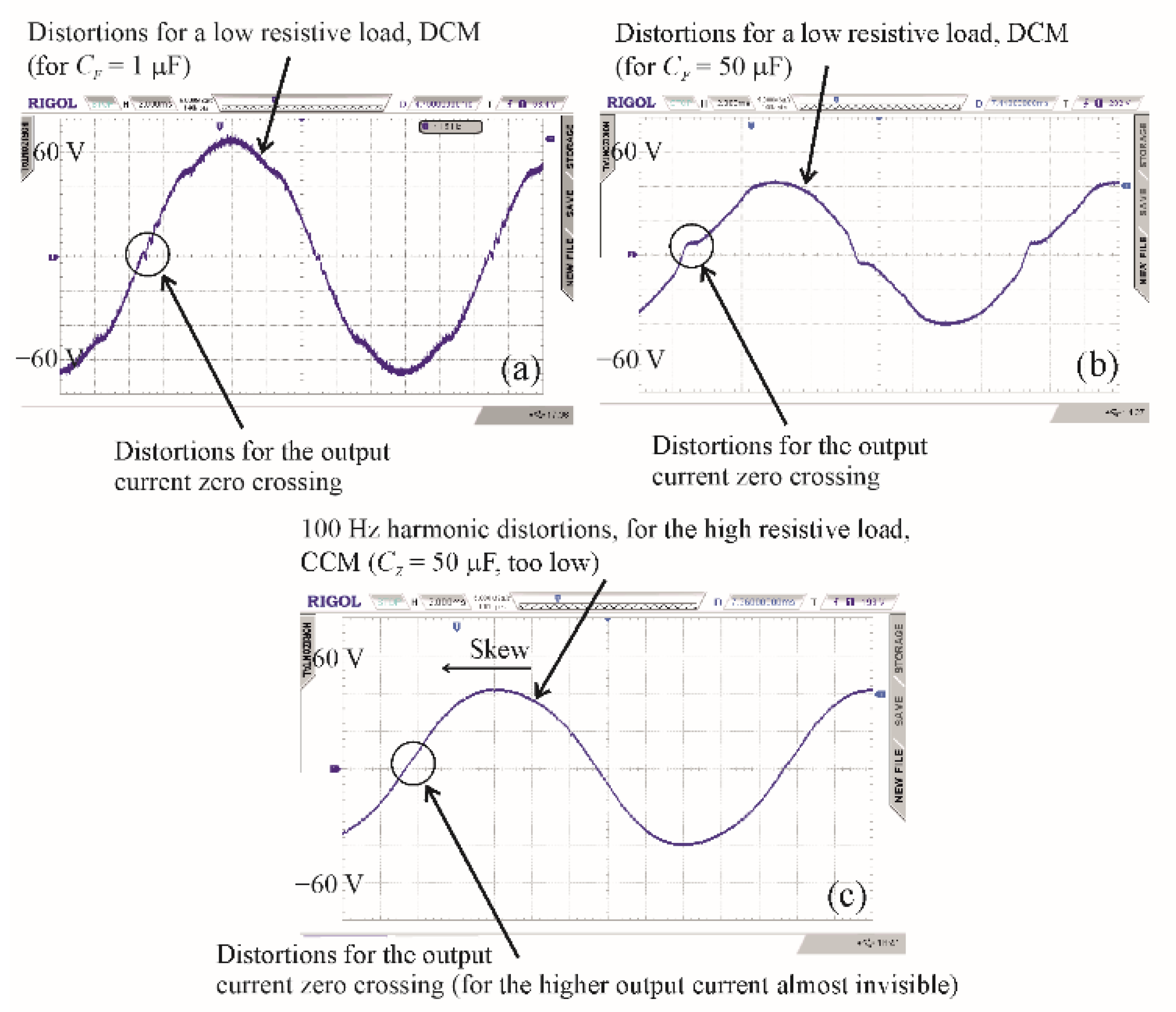
The basic structures of Z-source and qZ-source impedance networks are utilized today in photovoltaic systems [26]. The main disadvantage of these impedance networks lies in the discontinuous current mode (DCM) where the current in the inductors is equal to zero for a time period during Ts where there is a low load of the VSI and a low dZ coefficient. This is the main reason for the VSI output voltage distortions as shown in Figure 3a,b. By calculating a sufficiently large inductance of the coils [23,27,28] and selecting an appropriate magnetic material [29] for the lowest load while assuming the value of dZ, the current in the coils should not decrease to zero. During operation, it cannot be guaranteed that the load current will be nominal. Thus, the additional current taken from the impedance network is a solution of DCM omitting for a low load current.
Another reason for output distortions is the insufficient capacity of Z-source capacitors. Input current from a VSI bridge is like a “rectified” waveform that is filtered by the LC input network and is approximately the first harmonic of the “rectified” current at 100 Hz. This means that 100 Hz distortion is present in the 50 Hz output waveform as shown in Figure 3c. For the insufficient capacity, the output sinusoidal waveform is left-skewed [23,27]. The third type of VSI output distortions are observed after crossing zero output voltage caused by the additional voltage drops on the switched-on transistors during the shoot-through time (see Figure 3a–c), thus causing oscillations after a change of polarization in the PWM voltage. The impedance network influences the dynamic properties of an entire ZSI [23,27,28] which introduces additional resonant frequencies and the additional damping to the Bode plots of the ZSI. The main objective of this paper is to demonstrate how charging the battery from a DC-link after the impedance network during the non-shoot through times can reduce output distortions caused by the DCM of the impedance network. However, charging a battery with too high a current can lead to distortions of the output voltage after the voltage current is zero crossing and oscillations as the result of the higher voltage drops on the switches during the shoot-through time. Experimental results presented will show how charging the battery for a Z-source decreases the output of total harmonic distortions (THD) even in the case when a sophisticated feedback loop, for example, a passivity-based control (PBC), is used.
Figure 3 presents the different types of output voltage distortions of the ZSI. In Figure 3a,b, the DCM of the Z-source uses a low load current and ZSI output filter capacitors of CF = 1 μF and 50 μF respectively. Figure 3c shows the distortions caused by a 100 Hz current harmonic using a high load current and a Z-source capacitor of CZ = 100 μF.
Section 2 presents the basic structures of impedance networks and calculations of the minimum ZSI output current IOUTrmsmin that ensure their continuous current mode (CCM). In Section 3 the idea of the inverter with the impedance network charging the battery from the DC link (during non-shoot-through time) to keep the impedance network in CCM is presented. The simulations and results of the experimental verification are presented. Section 4 contains the discussion of what kind of previously presented types of ZSI output voltage distortions can be canceled by the controlled charging of the battery. Section 5 presents the final conclusions.
2. Basic Impedance Networks: Z-Source and qZ-Source
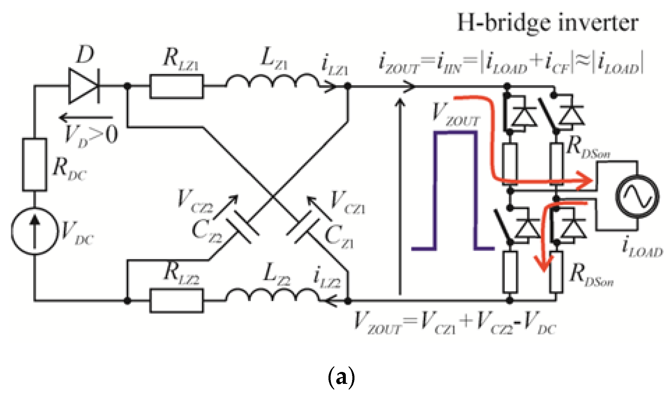
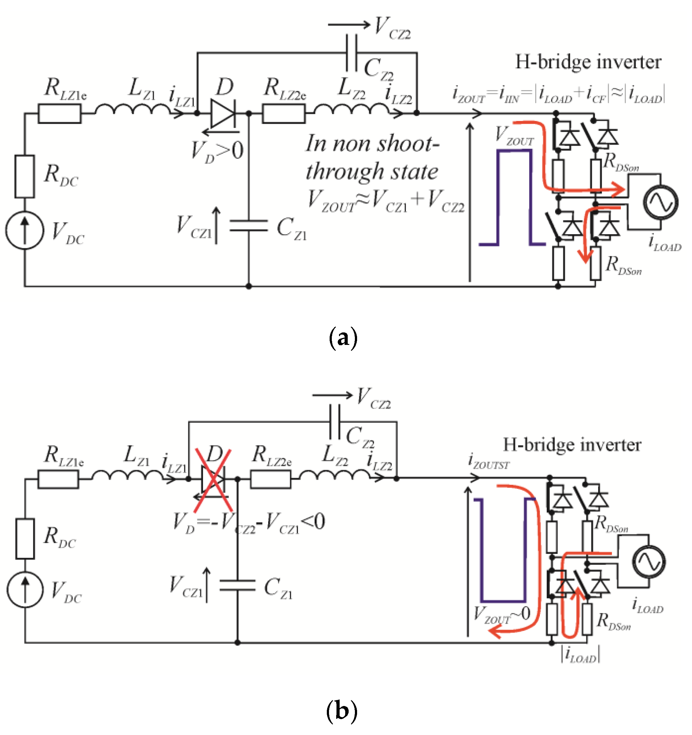
The Z-source and qZ-source impedance networks shown in Figure 1 and Figure 2, respectively, can operate in different states. Two basic states were taken into account during analysis and these include the shoot-through and the non-shoot-through states. The non-shoot-through state is depicted in Figure 1a and Figure 2a, while the shoot-through state [23,27,28] is shown in Figure 1b and Figure 2b.
The Z-source has a symmetrical structure where the values of the inductors are equal i.e., LZ1 = LZ2. Similarly, the values of capacitors are the same, i.e., CZ1 = CZ2, and the currents in both inductors are the same, i.e., iLZ1 = iLZ2. In the qZ-source, the currents in both coils are the same and are identical to the Z-source coils currents (neglecting the influence of the different parasitic resistances) if coils have equal inductances.
The amplitude of the VSI output voltage VOUTmax for the ZSI and qZSI is defined in Equation (1) as
where η is the efficiency, VDC is the input voltage, M is the VSI modulation coefficient, and kV’ is the DC voltage boost factor of the impedance network without power losses [23,27,28].
It is assumed that the capacitance CZ in the Z-source and qZ-source networks are sufficiently high. The average voltage on the capacitors of the Z-source and the CZ2 capacitor of the qZ-source are identical to the average voltage VLZav on the inductors [23,27,28] given in Equation (2) as follows:
The input power PIN and output power POUT of the VSI connected to the impedance networks for a Z-source or qZ-source can be calculated using Equations (3)–(5):
where ILZav is a single inductor current averaged over the fundamental period Tm.
For the simplest case of the resistive ZSI load, RLOAD the output power can be defined Equation (6) as
And the average inductor current ILZav for the root mean square (rms) value of the inverter output current IOUTrms is given Equation (7) as
The iLZ inductor current illustrated in Figure 4a comprises three components. These components are the average current ILZav, the current iLZ2fm which is averaged in the Ts switching period, and the triangle component iLZΔ of the inductor current. The current iLZ2fm has the double fundamental frequency caused by the envelope of the input current of the VSI bridge in the non-shoot-through time while the triangle component inductor current iLZΔ is caused by storing energy in the coil during the shoot-through time and recovering energy in the rest of the switching period (in CCM). A plot of the VSI input current is displayed in Figure 4b.
The inductor current iLZ is defined in Equation (8) as
Figure 4 shows plots of a Z-source or qZ-source impedance network coil current and an inverter input current including shoot-through current pulses for cases of maximum and close to zero crossing of the inverter output voltage (in CCM).
This most important harmonic component 2 fm of the VSI bridge input current flows through the LZCZ circuit of the impedance network as shown in Equation (9). It is assumed that all power losses are within the impedance network including the power losses on the VSI switches during the shoot-through time.
The triangle component iLZΔ of the inductor current iLZ in the CCM is calculated approximately with the assumption that a sufficiently low capacitor voltage ripple ΔVCZ is approximately equal to 0 and VCZmax is nearly equal to VCZav for the shoot-through time. The triangle component iLZΔ can thus be expressed in Equation (10) as
Consequently, the inductor current can be defined Equation (11) as
The lowest value of the inductor current is calculated Equation (12) as
As shown in Figure 4a, the requirement for CCM is that iLZmin must be greater than 0. This phenomenon is expressed in Equation (13) as
From Figure 5a, the absolute value of load impedance expressed in Equation (14) should be lower in value (but always positive) than the value calculated in Equation (14) for CCM for the assigned parameters: dZ, LZ, and CZ, M = 1 − dZ.
As shown in Figure 5b, the minimum output current for CCM is given Equation (15) as
The impedance network (Figure 5b) operates in the CCM for the ZSI load current IOUTrms higher than the value calculated from Equation (15) for assigned LZ = 1 mH and three parameters: VDC, dZ, and CZ. The modulation index M has the assigned maximum possible value M = 1 − dZ.
In Figure 6, the continuous current mode is illustrated where the output voltage of the ZSI is undistorted.
Figure 7 presents the DCM where two cases can be distinguished. From this figure, the distortions of the output voltage are small when the output voltage is below the maximum. When the output voltage is closer to the maximum, the distortions are higher, and the output voltage maximum is lower than expected. For the large VSI output capacitor the VSI output and PWM envelope voltages are shifted when the large VSI output capacitor e.g., CF = 50 μF is used. As shown in Figure 7, the short PWM pulses are undistorted in DCM while the wide pulses are distorted, and the output voltage is lower. The simulation of a DCM operation using the Z-source is presented in Figure 8 for the third PWM modulation schema [30]. The variables used to obtain the measured plots in Figure 8 are given as: CF = 1 μF, dZ = 0.3, M = 0.65, RLOAD = 1000 Ω, 3rd modulation schema.
3. Controlled Energy Flow—Charging the Battery
Similar results of measurement shown in Figure 7 and simulations in Figure 8 demonstrate that further simulations of the controlled energy flow i.e., charging the battery is useful. The basic solution is an efficient multi-input-single-output (MISO) [31] feedback that can decrease total harmonic distortions (THD) [23,27]. In addition, MISO feedback can decrease two other types of output voltage distortions [27]. However, for systems supplied by varying the DC supply voltage, for example, photovoltaic cells, the controlled energy flow to the batteries, which keeps the CCM, can be used. It is recommended that the battery is charged with a current that is a function of the difference between the calculated value of IOUTrmsmin and averaged (10 Hz low pass filter) VSI output current IOUTrms as shown in Figure 9 (if this difference is negative the charging battery current is equal to zero). The actual difference of these currents IOUTrmsmin − IOUTrms is recalculated (if positive) to match the required increase of the average ILZav current expressed in Equation (7). The battery can be charged only during the non-shoot-through state. Energy from the battery is discharged when VDC decreases below the assumed value of VDCmin, the Z-source is switched off and the shoot-through pulses are blocked.
The idea of this system is presented in Figure 9 (for switches placed in the position of discharging the battery). When the battery returns energy, the following happens: the shoot-through pulses are stopped, and the 48 V battery is connected directly to the VSI. This battery voltage should be higher than the amplitude of the output sinusoidal voltage and the modulation index M of VSI is increased i.e., M2 is greater than M1 (Figure 9).
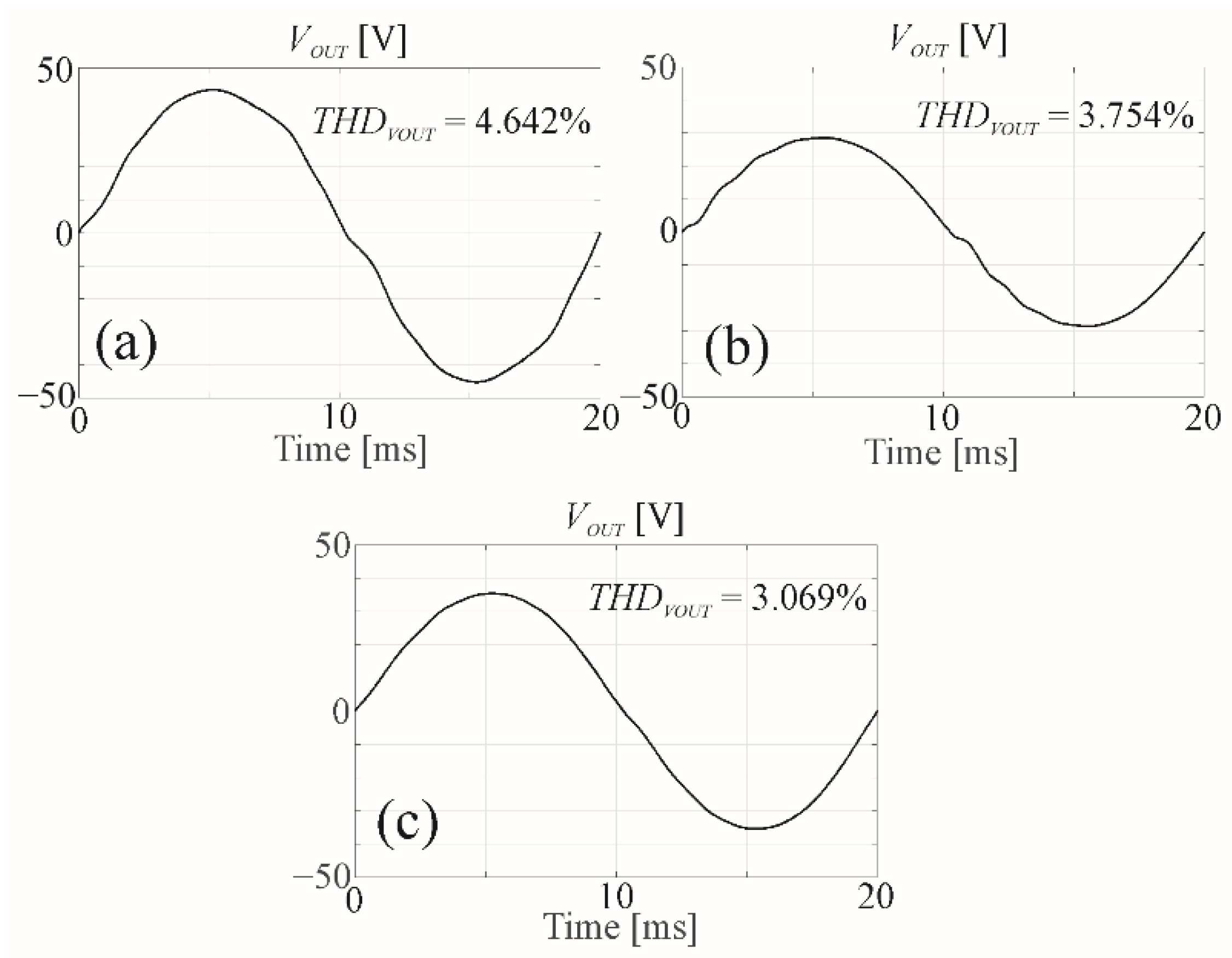
Figure 10a presents the simulated waveforms of the VDC changed 24/12/24 V (the border value is set to 15 V) with the described automatic action from Figure 9 but without controlled charging the battery when Z-Source operates in the DCM. The following parameters were used in this scenario: dZ = 0.3, M1 = 0.65, M2 = 0.75 and RLOAD = 1000 Ω. Figure 10b presents that same operation but with controlled charging of the battery for keeping Z-Source in the CCM. The current charging of the battery is calculated as IBATT = f(IOUTrmsmin − IOUTrms) using Equation (15), where f is a function of Equation (7). The battery charging current IBATT calculated from Equations (7) and (15) should be reduced because too high a value of the battery charging current leads to distortions of the VSI output voltage time after the output voltage is zero-crossing (see Figure 11b). These distortions are caused by the high voltage drops on the VSI switches during the shoot-through time. The presented (Figure 10b) reduction of the output voltage THD from 4.6% to 3% without any feedback loop is quite promising.
The presented simulations were verified in an experimental model using a 12 V battery (without discharging the battery) charged from the DC during dBTs pulses where (dB = 1 − dZ) (Figure 12). The feedback loop was the IPBC2 type presented in [27]. For the DCM mode of the Z-source, the output voltage distortions can be reduced by additional loading the impedance network by means of charging the battery from the DC link in the non-shoot through times.
The current source from Figure 9 was simply substituted with resistors. Charging the battery allowed for a substantial reduction of output voltage THD from 2.63% to 0.9%. for IBATT = 120 mA, but THD increased to 0.97% for IBATT = 200 mA. Further research will be on the use of battery charging current not only to reduce the distortions of the output voltage but also looking for a maximum power point (MPP) when the impedance network is supplied from the photovoltaic cell. The battery charging current can be controlled by the coefficient dB for the input current of the impedance network would be closer to MPP.
4. Discussion
The presented results of the simulation and measurements of the experimental ZSI proved that charging the battery from the DC link between impedance network and VSI in the non-shoot-through time can seriously decrease the ZSI output voltage distortions keeping the impedance network in the CCM. The controlled energy flow solution is particularly predicted for the case of wide variations of the input DC voltage and variations of the load current. The output voltage distortions are decreased even when a strong feedback loop of the VSI is present. The controlled charging of the battery can help in the maximum power point tracking when the ZSI is supplied from the photovoltaic cell and this is the perspective of the further studies. In [23], three types of VSI output voltage distortions were distinguished. The controlled charging of the battery can cancel one of them but setting too high a value of this current increases the other reason for distortions. Charging the battery from the DC link of the ZSI during the non-shoot-through time was not presented yet, however, another approach to the controlled power flow for qZSI with charging the battery connected parallel to the CZ2 capacitor (Figure 2) was presented in [32].
5. Conclusions
In this paper, a technique has been proposed to reduce output voltage distortions in voltage source inverters connected to impedance networks. The proposed method has been validated using simulations and experimentally under different operating conditions. It was discovered that by connecting a rechargeable battery to a DC link placed between an impedance network and a VSI and employing proper control of the battery charging current during the non-shoot through time, the output voltage distortions in a system with or without feedback can be reduced when a continuous current mode of the impedance network is forced. However, too high a current charging the battery may increase other types of VSI output voltage distortions presented in Figure 11b caused by high voltage drops on the VSI switches during the shoot-through time. Furthermore, the battery charging current can be controlled to increase the impedance network input current to enable the system to reach the maximum power point when the DC source is a photovoltaic cell. The results presented in this paper thus demonstrate that the proposed method is suitable and can be applied in practice to real-time supply systems.
Author Contributions
Conceptualization, Z.R.; methodology, Z.R. and K.B.; software, Z.R.; validation, Z.R., K.B. and Ł.D.; formal analysis, Z.R. and K.B.; investigation, Z.R. and K.B.; resources, Z.R. and K.B.; data curation, Z.R. and K.B.; writing—original draft preparation, Z.R.; writing—review and editing, Z.R. and K.B.; visualization, Z.R.; supervision, Z.R.; project administration, Z.R. and K.B.; funding acquisition, Z.R. and K.B. All authors have read and agreed to the published version of the manuscript.
Funding
This work was partly supported by the Polish Ministry of Science and Higher Education funding for statutory activities.
Conflicts of Interest
The authors declare no conflict of interest. The funders had no role in the design of the study; in the collection, analyses, or interpretation of data; in the writing of the manuscript, or in the decision to publish the results.
References
- Peng, F.Z. Z-Source Inverter. IEEE Trans. Ind. Appl. 2003, 39, 504–510. [Google Scholar] [CrossRef]
- Anderson, J.; Peng, F. Four quasi-Z-Source inverters. Proc. IEEE Power Electron. Spec. Conf. 2008, 2743–2749. [Google Scholar] [CrossRef]
- Li, Y.; Peng, F.Z. AC Small Signal Modeling, Analysis and Control of Quasi-Z-Source Converter. In Proceedings of the 2012 IEEE 7th International Power Electronics and Motion Control Conference—ECCE Asia, Harbin, China, 2–5 June 2012; pp. 1848–1854. [Google Scholar] [CrossRef]
- Liu, W.; Yang, Y.; Kerekes, T.; Liivik, E.; Blaabjerg, F. Impedance Network Impact on the Controller Design of the QZSI for PV Applications. In Proceedings of the 2020 IEEE 21st Workshop on Control and Modeling for Power Electronics (COMPEL), Aalborg, Denmark, 9–12 November 2020. [Google Scholar] [CrossRef]
- Subhani, N.; Kannan, R.; Mahmud, A.; Blaabjerg, F. Z-source inverter topologies with switched Z-impedance networks: A review. IET Power Electron. 2021, 14, 727–750. [Google Scholar] [CrossRef]
- Zhu, M.; Yu, K.; Luo, F.L. Switched Inductor Z-Source Inverter. IEEE Trans. Power Electron. 2010, 25, 2150–2158. [Google Scholar] [CrossRef]
- Itozakura, H.; Koizumi, H. Embedded Z-Source Inverter with Switched Inductor. In Proceedings of the IECON 2011—37th Annual Conference of the IEEE Industrial Electronics Society, Melbourne, VIC, Australia, 7–10 November 2011; pp. 1342–1347. [Google Scholar] [CrossRef]
- Adamowicz, M.; Guzinski, J.; Strzelecki, R.; Peng, F.Z.; Abu-Rub, H. High Step-Up Continuous Input Current LCCT-Z-Source Inverters for Fuel Cells. In Proceedings of the Energy Conversion Congress and Exposition (ECCE), Phoenix, AZ, USA, 17–22 September 2011; pp. 2276–2282. [Google Scholar] [CrossRef]
- Adamowicz, M. LCCT-Z-Source Inverters. In Proceedings of the 10th International Conference on Environment and Electrical Engineering, Rome, Italy, 8–11 May 2011; pp. 1–6. [Google Scholar] [CrossRef]
- Vinnikov, D.; Roasto, I.; Strzelecki, R.; Adamowicz, M. Step-Up DC/DC Converters With Cascaded Quasi-Z-Source Network. IEEE Trans. Ind. Electron. 2012, 59, 3727–3736. [Google Scholar] [CrossRef]
- Siwakoti, Y.P.; Blaabjerg, F.; Galigekere, V.P.; Ayachit, A.; Kazimierczuk, M.K. A-Source Impedance Network. IEEE Trans. Power Electron. 2016, 31, 8081–8087. [Google Scholar] [CrossRef]
- Hakemi, A.; Sanatkar-Chayjani, M.; Monfared, M. Δ-Source Impedance Network. IEEE Trans. Ind. Electron. 2017, 64, 1–10. [Google Scholar] [CrossRef]
- Rezazadeh, H.; Monfared, M.; Nikbahar, A.; Sharifi, S. A family of high voltage gain quasi-Δ-source impedance networks. IET Power Electron. 2021, 14, 807–820. [Google Scholar] [CrossRef]
- Siwakoti, Y.P.; Peng, F.Z.; Blaabjerg, F.; Loh, P.C.; Town, G.E. Impedance-Source Networks for Electric Power Conversion Part I: A Topological Review. IEEE Trans. Power Electron. 2015, 30, 699–716. [Google Scholar] [CrossRef]
- Reddivari, R.; Jena, D. A Correlative Investigation of Impedance Source Networks: A Comprehensive Review. IETE Tech. Rev. 2021, 38, 1–34. [Google Scholar] [CrossRef]
- Ghasimi, S.; Eshkevari, A.L.; Mosallanejad, A. A high-gain IΓ-source hybrid single-phase multilevel inverter for photovoltaic application. IET Power Electron. 2021, 14, 106–119. [Google Scholar] [CrossRef]
- Kumar, A.; Bao, D.; Beig, A.R. Comparative Analysis of Extended SC-qSBI with EB-QZSI and EB/ASN-QZSI. IEEE Access 2021, 9, 61539–61547. [Google Scholar] [CrossRef]
- Zhao, P.; Wang, J.; Hao, H.; Wang, U. Y-Source Two-Stage Matrix Converter and Its Modulation Strategy. IEEE Access 2020, 8, 214282–214292. [Google Scholar] [CrossRef]
- Yuan, J.; Mostaan, A.; Yang, Y.; Siwakoti, Y.P.; Blaabjerg, F. A Modified Y-Source DC–DC Converter With High Voltage-Gains and Low Switch Stresses. IEEE Trans. Power Electron. 2020, 35, 7716–7720. [Google Scholar] [CrossRef]
- Gayen, P.K. An enhanced high-boost active-switched quasi Z-Source inverter having shorter range of shoot-through duty ratio for solar energy conversion applications. AEU—Int. J. Electron. Commun. 2021, 137, 153822. [Google Scholar] [CrossRef]
- Siwakoti, Y.P.; Peng, F.Z.; Blaabjerg, F.; Loh, P.C.; Town, G.E.; Yang, S. Impedance-Source Networks for Electric Power Conversion Part II: Review of Control and Modulation Techniques. IEEE Trans. Power Electron. 2015, 30, 1887–1906. [Google Scholar] [CrossRef]
- Abdelhakim, A.; Blaabjerg, F.; Mattavelli, P. Modulation Schemes of the Three-Phase Impedance Source Inverters—Part I: Classification and Review. IEEE Trans. Ind. Electron. 2018, 65, 6309–6320. [Google Scholar] [CrossRef]
- Rymarski, Z.; Bernacki, K. Drawbacks of impedance networks. Int. J. Circuit Theory Appl. 2018, 46, 612–628. [Google Scholar] [CrossRef]
- Bernacki, K.; Rymarski, Z. Electromagnetic Compatibility of Impedance Source Inverters. Elektron. Elektrotechnika 2017, 23, 55–63. [Google Scholar] [CrossRef] [Green Version]
- Hufman, B. Efficiency and Power Characteristics of Switching Regulator Circuits. Linear Technol. Appl. Note 1991, 46, 1–28. [Google Scholar]
- Ge, B.; Abu-Rub, H.; Peng, F.Z.; Lei, Q.; Almeida, A.T.; Ferreira, F.J.T.E.; Sun, D.; Liu, Y. An Energy-Stored Quasi-Z-Source Inverter for Application to Photovoltaic Power System. IEEE Trans. Ind. Electron. 2013, 60, 4468–4481. [Google Scholar] [CrossRef]
- Rymarski, Z.; Bernacki, K.; Dyga, Ł. Decreasing the single phase inverter output voltage distortions caused by impedance networks. IEEE Trans. Ind. Appl. 2019, 55, 7586–7594. [Google Scholar] [CrossRef]
- Rymarski, Z.; Bernacki, K. Influence of Z-Source output impedance on dynamic properties of single-phase voltage source inverters for uninterrupted power supply. IET Power Electron. 2014, 7, 1978–1988. [Google Scholar] [CrossRef]
- Bernacki, K.; Rymarski, Z.; Dyga, Ł. Selecting the coil core powder material for the output filter of a voltage source inverter. Electron. Lett. 2017, 53, 1068–1069. [Google Scholar] [CrossRef]
- Bernacki, K.; Rymarski, Z. Electromagnetic compatibility of voltage source inverters for uninterruptible power supply system depending on the pulse-width modulation scheme. IET Power Electron. 2015, 8, 1026–1034. [Google Scholar] [CrossRef]
- Astrom, K.J.; Wittenmark, B. Computer-Controlled Systems: Theory and Design, 3rd ed.; Dover Publications Inc.: Mineola, NY, USA, 2011; ISBN 9780486486130. [Google Scholar]
- Sun, D.; Ge, B.; Peng, F.Z.; Abu Rub, H.; de Almeida, A.T. Power flow control for quasi-Z source inverter with battery based PV power generation system. In Proceedings of the 2011 IEEE Energy Conversion Congress and Exposition, Phoenix, AZ, USA, 17–22 September 2011; pp. 1051–1056. [Google Scholar] [CrossRef]
Figure 1.
(a) Non-shoot-through state and (b) shoot-through state of the Z-source impedance network with the VSI.
Figure 1.
(a) Non-shoot-through state and (b) shoot-through state of the Z-source impedance network with the VSI.


Figure 2.
(a) Non-shoot-through state and (b) shoot-through state of the qZ-source impedance network with the VSI.
Figure 2.
(a) Non-shoot-through state and (b) shoot-through state of the qZ-source impedance network with the VSI.

Figure 3.
Inverter output voltage distortions, (a) Z-source in DCM using a VSI output filter capacitor CF = 1 μF, (b) Z-source in DCM using a VSI output filter capacitor CF = 50 μF, (c) 100 Hz harmonic distortions with a Z-source capacitor CZ = 100 μF.
Figure 3.
Inverter output voltage distortions, (a) Z-source in DCM using a VSI output filter capacitor CF = 1 μF, (b) Z-source in DCM using a VSI output filter capacitor CF = 50 μF, (c) 100 Hz harmonic distortions with a Z-source capacitor CZ = 100 μF.

Figure 4.
A Z-source or qZ-source impedance network (a) coil current and (b) the VSI input current including shoot-through current pulses (that do not supply inverter) in the case of wide (for the maximum of the output inverter voltage) and short (close to zero crossing of the output inverter voltage) inverter PWM pulses in the CCM.

Figure 5.
(a) Maximum load impedance, and (b) minimum output current, that keeps the impedance network in the continuous current mode.
Figure 5.
(a) Maximum load impedance, and (b) minimum output current, that keeps the impedance network in the continuous current mode.

Figure 6.
CCM waveforms of (a) the ILZ coil current, ZSI output voltage, and inverter PWM pulses, and (b) the undistorted inverter output voltage.
Figure 6.
CCM waveforms of (a) the ILZ coil current, ZSI output voltage, and inverter PWM pulses, and (b) the undistorted inverter output voltage.

Figure 7.
Measured DCM waveforms of the LZ coil current, ZSI output voltage, and the inverter’s PWM wide and short pulses for CF = 1 μF and 50 μF inverter capacitors.
Figure 7.
Measured DCM waveforms of the LZ coil current, ZSI output voltage, and the inverter’s PWM wide and short pulses for CF = 1 μF and 50 μF inverter capacitors.

Figure 8.
Simulated DCM waveforms for inverter CF = 1 μF, dZ = 0.3, M = 0.65, RLOAD = 1000 Ω, 3rd modulation schema.
Figure 8.
Simulated DCM waveforms for inverter CF = 1 μF, dZ = 0.3, M = 0.65, RLOAD = 1000 Ω, 3rd modulation schema.

Figure 9.
Proposed idea of the inverter with the impedance network charging the battery from the DC link (during non-shoot-through time), and automatic switching to supplying directly from the battery (the positions of switches are presented in the position of discharging the battery when VDCmin − VDC > 0).

Figure 10.
The waveforms of the DC input and AC output voltages of the ZSI switched from a mode of supplying the VSI from Z-source to the mode of supplying VSI from the battery in case of the low input DC voltage, (a) without controlled charging battery for Z-source in the DCM for the low load, and (b) with controlled charging battery for Z-source in CCM.

Figure 11.
Inverter output voltage (a) without charging battery, (b) the battery charging current directly equal to f(IOUTrmsmin − IOUTrms), where f is a Equation (7), and (c) the battery charging with the reduced value of current.
Figure 11.
Inverter output voltage (a) without charging battery, (b) the battery charging current directly equal to f(IOUTrmsmin − IOUTrms), where f is a Equation (7), and (c) the battery charging with the reduced value of current.

Figure 12.
(a) The inverter experimental set up and (b) inverter output voltage distortions comparison for an IPBC controller where RLOAD = 2000 Ω, RMS battery charging currents: IBATT = 0 (DCM of the Z-source), IBATT = 120 mA and IBATT = 200 mA (CCM of the Z-source), dZ = 0.3, and dB = 1 − dZ—battery charging pulses coefficient.


Publisher’s Note: MDPI stays neutral with regard to jurisdictional claims in published maps and institutional affiliations. |
© 2021 by the authors. Licensee MDPI, Basel, Switzerland. This article is an open access article distributed under the terms and conditions of the Creative Commons Attribution (CC BY) license (https://creativecommons.org/licenses/by/4.0/).
Share and Cite
MDPI and ACS Style
Rymarski, Z.; Bernacki, K.; Dyga, Ł. Controlled Energy Flow in Z-Source Inverters. Energies 2021, 14, 7272. https://0-doi-org.brum.beds.ac.uk/10.3390/en14217272
AMA Style
Rymarski Z, Bernacki K, Dyga Ł. Controlled Energy Flow in Z-Source Inverters. Energies. 2021; 14(21):7272. https://0-doi-org.brum.beds.ac.uk/10.3390/en14217272
Chicago/Turabian StyleRymarski, Zbigniew, Krzysztof Bernacki, and Łukasz Dyga. 2021. "Controlled Energy Flow in Z-Source Inverters" Energies 14, no. 21: 7272. https://0-doi-org.brum.beds.ac.uk/10.3390/en14217272
Note that from the first issue of 2016, this journal uses article numbers instead of page numbers. See further details here.