Review on the Sources of Power Loss in Monofacial and Bifacial Photovoltaic Technologies


1
School of Energy, Geoscience, Infrastructure and Society, Heriot-Watt University, Edinburgh EH14 4AS, UK
2
School of Energy, Geoscience, Infrastructure and Society, Heriot-Watt University, Dubai P.O. Box 38103, United Arab Emirates
*
Author to whom correspondence should be addressed.
Energies 2021, 14(23), 7935; https://0-doi-org.brum.beds.ac.uk/10.3390/en14237935
Submission received: 22 October 2021
/
Revised: 18 November 2021
/
Accepted: 23 November 2021
/
Published: 26 November 2021
(This article belongs to the Special Issue Energy Efficiency, Low Carbon Resources and Renewable Technology)
Abstract
:An evaluation of the degradation effects on photovoltaic modules is essential to minimise uncertainties in the system operation. Bifacial photovoltaic technology is attracting attention due to the capacity of generating energy from the front and rear sides. This paper presents a review of degradation factors, for both conventional monofacial and bifacial photovoltaic modules, to highlight how the current and voltage characteristics of these technologies are affected by degradation. Microcracking, encapsulant discoloration, and light induced degradation seem to have similar effects on both modules. Contrarily, bifacial modules are more prone to potential induced degradation as the electromagnetic shielding is affected by the bifaciality. Bifacial devices are less affected by light and elevated temperature induced degradation. The degradation (1.3%) is similar for both technologies, up to 40 kWh/m of solar radiation. Above this value, monofacial degradation increases faster, reaching values of 7%. For tilted systems, the front side soiling degradation of 0.30% per day is similar for both technologies. For vertical systems, soiling loss for bifacial is considerably lower with values of 0.02% per day.
1. Introduction
Solar photovoltaic (PV) energy is one of the most promising renewable energy sources. It occupies the second largest portion of the global installed capacity of renewable energy [1]. This energy source has experienced significant growth in the last decade, coming from a total installed capacity of 40.29 GW in 2010 to 707.5 GW in 2020 [2]. The search for reducing the costs and improving the efficiency of PV systems has led to the development of different materials, modules, and system designs. The different materials and technologies that show a significant improvement of efficiency for a small cost, are quickly introduced to the PV market. This results in many PV systems been installed without sufficient understanding regarding their long term durability and reliability. Therefore, it can lead to an unexpected degradation, which compromises the longevity of the whole system and affect the Levelised Costs of Energy (LCOE) [3] by the reduction of the energy yield and/or by the increase of the operating expenditure (OPEX).
A recent fast-growing technology is bifacial PV (BPV) modules. This technology has attracted market attention and is expected to be the next breakthrough technology in the field [4]. Currently, BPV corresponds to approximately 20% of the market share of PV technologies. This number is expected to increase to 70% by 2030 [5]. This increasing interest arises from the BPV capacity to convert additional solar irradiance from the rear side, which allows it to obtain a higher energy yield compared to monofacial technology, especially for PV systems installed in areas with a high albedo and high latitudes [6]. This energy gain between monofacial PV (MPV) and BPV technologies is determined by the bifacial gain, which is the ratio between the power produced by bifacial cells/modules and the power produced by monofacial cells/modules [4]. For smaller bifacial systems, bifacial gain ranges from 15 to 25% and 5 to 15% for larger commercial systems [7,8,9]. Additionally, the fabrication of BPV modules does not require significant changes in the current process of fabrication of monofacial modules. It is estimated that the average additional cost for BPV modules is 3% [10], therefore representing a small increase in the capital expenditure (CAPEX) but generating a higher energy yield [10].
The lifetime of a PV module is expected to be from 20 to 30 years [11]. Throughout this period, certain limits for the power output reduction are considered acceptable, such as a maximum reduction of 10% of the initial power output after the first 10 years of operation, and 20% of the initial power after the first 25 years [12]. This power output reduction over the years is known as degradation rate and is an important factor for stakeholders as it directly impacts the amount of energy produced. The degradation rate can change according to many factors such as environmental conditions and handling of the modules. Therefore, an accurate prediction of the losses as the module ages is essential to promote the growth of this industry. The process of estimating the performance includes the module’s efficiency in outdoor conditions and also the analysis of how this efficiency decreases over time due to degradation of materials and components [12], as well as other factors such as soiling, mismatch, and partial shading.
In operation, PV modules are vulnerable to diverse degradation phenomena such as encapsulant yellowing, microcracks, metal contacts detaching, breaking and rusting, light-induced degradation, and potential induced degradation [13]. It is important to have a deep understanding of the degradation rate as it can eventually lead to module failure or, in case of the underestimation of the degradation rate, lead to an increase in the financial risk [14]. For MPV, the average degradation rate per year is approximately 0.36% for mono-crystalline silicon and 0.64% for multi-crystalline silicone [14]. Although it is not yet widely explored in the literature, the degradation rate for bifacial PV of the system is normally under 1% per year [15]. However, studies have shown that in extreme conditions, under high temperatures and irradiances in desert conditions, the overall degradation can reach nearly 2% [16].
Another factor that causes a significant drop in the power output is the mismatch effect, which represents the non-identical current and voltage characteristics of PV cells within a module or in a string [6,17]. This effect occurs because the current and voltage (I-V) characteristics of the cells within a module are never identical and worsen when the cells are exposed to different levels of irradiance and temperature. It is an important issue in PV systems that needs to be taken into account in any PV installation as cells connected in series do not perform at their specific maximum power point simultaneously. The performance of a PV module is expressed as a collective maximum point instead [17]. The consequences of mismatches can be temporary or permanent depending on their intensity. It can affect the power output of the PV modules by shifting the module’s operating point further away from the ideal maximum power point [18]. Additionally, it can potentially affect the reliability of the PV system by leading to a reverse bias built up across the mismatched cell. This can make the weak cell start to behave as a load, sinking the current generated by the other cells, which can cause a significant increase in the cell’s operating temperature [18,19,20]. If the reverse bias voltage is higher than the breakdown voltage of the cell, potentially irreversible damage might occur as a large current concentrates in one specific area. This can originate a thermal breakdown of the cell, known as ‘Hot Spot’. Some consequences of this significant increase in temperature are the burning the ethylene-vinyl acetate (EVA) and/or back-sheet as well as the delamination of the encapsulated materials [18].
Though the manufacturing costs of crystalline silicon (C-Si), which includes both MPV and BPV modules, has decreased significantly, the actual performance and viability of the system are expressed by the Levelised Cost of Energy (LCOE). The LCOE is a relation between the sum of CAPEX and OPEX (which represent the life cycle costs of the system) and the lifetime electricity generation (yield) [21]. Thus, understanding the degradation of PV modules and the power output losses of MPV and BPV modules in operation is of great importance for an accurate prediction of the system viability and to enable manufacturers to find alternatives to improve materials and processes to prevent premature ageing, degradation, and failure. Therefore, reducing the total energy generation and lifetime of the module. This degradation and mismatch may cause the module to perform under the expected power rating informed in their data-sheets. Therefore, to enable the widespread of solar PV systems it is necessary to accurately estimate the real performance and the losses involved in the energy conversion process. A deeper study in this area is essential as most software available in the market for PV systems simulation (e.g., PVSyst [22], SAM [23] and PV*Sol [24]) consider these losses as a constant value over the year.
The literature to date lacks information comparing the degradation of MPV and BPV modules. The losses caused by different degradation affect each PV module technology differently. Therefore, to promote the adoption of BPV technology, it is necessary to understand how resilient this technology is regarding the short and long term losses due to degradation and mismatch. The contribution in this work provides a comprehensive review of the state-of-the-art regarding the degradation and mismatch that directly affect the performance of crystalline silicon PV cells and modules. A comparison of BPV and MPV losses for each degradation is provided wherever available. This review aims to provide a better understanding of the losses involved in the energy conversion process, semiconductor internal losses, and the environmental effect on the performance of these two module technologies, thereby allowing a better estimation for the LCOE.
The next section introduces the current-voltage curve parameters that represent the performance of a solar cell and the effect of losses. Section 3 describes the environmental factors that affect the performance of a PV system as well as the effects of internal ohmic losses within the semiconductor and metal contacts. Finally, Section 4 describes the main degradation effects that contribute to the increase of losses in monofacial and bifacial PV cells followed by the conclusions.
2. I-V Curve Parameters
The most used method to analyze the performance of a PV device is by the measurement of the current and voltage characteristics. In this method, a known irradiance is applied to the solar cell at a known temperature while it is connected to a variable resistive load. This load varies from the short circuit condition to the open circuit condition while both the voltage in the output terminals of the PV cell and the output current are measured [25]. The current and voltage curve represents a diagnostic of the characteristics of the photovoltaic device under certain levels of irradiance and temperature. A detailed analysis of these curves is essential to understand the physical phenomena that happen internally in the PV device under different external scenarios. The I-V curve of a solar cell presents important information about the performance of the device such as open-circuit voltage (), short-circuit current (), maximum power current () and voltage (), efficiency (), and fill factor () as shown in Figure 1. These parameters are essential for the testing, calibration, commissioning, design, fabrication, maintenance, and controlling of a photovoltaic system [26].
The open-circuit voltage represents the voltage between the terminals of the PV cell/module without any load connected to it (open circuit condition in the PV device’s terminals). At this voltage, there is no output current. The short-circuit current represents the current flowing through the short-circuited terminals when the voltage at the terminals is zero. The maximum power current and voltage represent the current and voltage levels that provide the highest power output as can be seen in Figure 2.
The I-V curve also shows parameters that represent the efficiency () and fill factor () of the cell, which indicates how efficient the cell is at power conversion. The efficiency is defined by the relation between the maximum power generated () and the total irradiance incident on the area of the cell, as can be seen in Equation (1). The fill factor represents the quality of the solar cell. It is obtained by the relation between the maximum power () and the theoretical power () as can be seen in Equation (2).
Please refer to Table 1 for the list of used symbols.
To estimate the performance of PV cells, electrical models with solar cell equivalent circuits are used to obtain the output parameters of the cells. One of the most widely used circuits is the single diode model, which is shown in Figure 3. This equivalent circuit is composed of a current source representing the photocurrent, a reverse-biased diode, a series, and a shunt resistance. For BPV modules, the equivalent circuit can be adapted, as seen in Figure 3b, which has an additional current source representing the front side photocurrent and rear side photocurrent separately [21]. The single diode model has been widely validated to emulate the performance of MPV modules [27,28,29,30,31] although, for BPV, despite it being used in few researches [31,32,33], its accuracy has not been widely explored.
For this model, Equation (3) represents the current-voltage relation of a silicon PV cells connected in series forming a PV module.
Please refer to Table 2 for the list of used symbols.
3. Factors That Impact on the I-V Curve
In operation, solar cells are exposed to different environmental conditions such as variable temperature and irradiance intensities. The current, voltage, and efficiency of MPV and BPV vary according to these environmental parameters and internal losses caused by parasitic resistances and degradation [34,35]. The performance parameters of a solar cell using the single diode model mentioned previously (i.e., open-circuit voltage, short-circuit current, photocurrent, series and shunt resistances, fill factor and efficiency) depend directly on the irradiance and temperature to which the cell is exposed to as well as the ohmic losses [35]. The effects of the increase of series resistance and decrease of shunt resistance can cause premature degradation of the PV device, which can cause temporary power reduction or permanent damage [35].
3.1. Ohmic Losses
3.1.1. Series Resistance
The series resistance represents the sum of several losses within a PV cell or module. This resistance can increase due to many degradation mechanisms such as metal contacts corrosion, junction box contacts, and defects of the interconnections between cells [35]. These losses can be in the semiconductor, metal connections, metallization process, and bus bar between the cells within a PV module. The increase of the series resistance deforms the cell’s I-V curve by increasing the voltage slope of the device, as shown in Figure 4.
3.1.2. Shunt Resistance
The shunt resistance represents the equivalent of any parallel high conductivity path that may occur across the solar cell semiconductor p-n junction. Ideally, the higher the value of this resistance the better. The reduction of shunt resistance deforms the shape of the I-V curve of the cell by increasing the current slope, as shown in Figure 5. This resistance is also known as leakage current resistance; when its value decreases, more leakage current starts flowing through the shunt paths and therefore the output current provided to a load circuit is reduced significantly [36]. As a result, the power output, efficiency, and fill factor are reduced as shown in [36].
3.2. Environmental Factors
3.2.1. Irradiance
The irradiance variation affects the generated current more significantly than the voltage. The current increases with the increase of solar irradiance incident on the surface of the cell, as shown in Figure 6.
In Crystalline Silicon solar cells, parameters such as short-circuit current, photocurrent, and diode ideality factor increase linearly with the irradiance levels, while the open-circuit voltage and efficiency increase logarithmically, and the saturation current increases exponentially. The shunt resistance increases slightly with the increase of irradiance levels until a certain point (<500 W/m) from which it becomes a constant. Studies shows that the fill factor for these cells increase with the increase of irradiance up to a certain point (<500 W/m) then it decreases almost linearly due to the effects of the series resistance. Regarding the resistances, the shunt resistance decreases linearly while the series resistance does not present a significant variation [37,38,39,40]
The effects of the irradiance incident on BPV is more complex than MPV. The BPV module’s rear side generally presents a distorted rear side I-V characteristic due to the self-shading effect caused by junction box, cabling, frame, label and mounting frame [41]. Additionally, the rear side irradiance is mainly composed of diffuse and reflected irradiance which makes it likely to be non-uniform [42]. According to the IEC TS 60904-1-2 [43], the characterisation process of BPV can be performed with single-side illumination or bifacial illumination. Schmid et al. [41] performed a comparison between these two methods and results show that the deviation of the short circuit current () obtained from each method was below . The open-circuit voltage () obtained did not present significant changes according to the method used. Additionally, this study has shown that for low irradiance levels the maximum power point () is more affected in the single-side illumination method. This occurs due to the effect of the shunt resistance, which is described in Section 3.1.2. Although, for higher irradiance levels of the bifacial illumination, the power output is lower due to the effect of the series resistance.
3.2.2. Temperature
The irradiance incident on the PV module can be absorbed by the cell or transmitted through it. The fraction of the irradiance transmitted is mostly IR (or near) light and it can be conducted through and out of the module, absorbed or reflected back to the cell. The portion of the solar irradiance absorbed by the solar cell is partially converted into electricity and heat due to conversion losses. The higher module’s operating temperature compared to the ambient temperature comes from the wasted energy generated during the photovoltaic energy conversion. From the irradiance incident on the surface of the PV panel, approximately only 20% is converted into electricity. The majority of the wasted energy is converted into heat [44]. This heat impacts directly on the power output of the modules and their efficiency. Many authors consider that parameters such as open-circuit voltage, short-circuit current and maximum power voltage vary linearly with the temperature [45,46,47,48]. The temperature has very little effect on the current although the increase in temperature shows a significant reduction of the open-circuit voltage, maximum power and Fill Factor [44,45,49,50], as shown in Figure 7. In the worst cases, the long time high operating temperature condition can cause irreversible degradation effects.
As BPV are capable of absorbing extra irradiance from their rear side, some researchers argue that the operating temperature of BPV is higher than MPV [51]. However, others defend that the BPV operating temperature is cooler compared to MPV due to the higher infrared (IR) light transmission through a BPV [52,53]. Lamers et al. [52], compared the heat balance of a monofacial Al-BSF solar cell, a white back sheet, and a glass-glass bifacial n-PERT solar cell. Results indoors show that the glass-glass structure presented a 12% higher effective heat compared to MPV with white back sheet when illuminated with 1000 W/m on the front and 200 W/m on the rear side. Although, in outdoor operating conditions, the glass-glass bifacial module presents a lower temperature than MPV, especially under high levels of irradiance, despite the higher power output and the higher effective heat input. Although, BPV modules suffer the effects of the self-shading on the rear side due to connections, frame, and mounting structure, which might affect the operating temperature of the modules. It is expected that glass-glass BPV modules present a less significant self-shading effect due to the absence of a frame. Both bifacial modules types (glass-glass and glass-foil) present a considerable temperature non-uniformity at different points of the module’s area. As presented by Kenny et al. [54], this non-uniformity can reach approximately 6 C and vary throughout the day.
4. PV Module Degradation
The term degradation is defined as a gradual deterioration of the characteristics of a material, component, or system. This deterioration may cause an impact on the system capacity to operate within the expected limits and therefore impact directly on their operating conditions [13]. For crystalline silicon solar cells (c-Si), the most frequent degradation causes are the discolouration of the encapsulant, microcracks, potential induced degradation (PID), light-induced degradation (LID) and light and elevated temperature degradation (LeTID). These types of degradation will be described in more details in the following subsections.
4.1. Encapsulant Discoloration and Delamination
C-Si PV modules correspond to the largest proportion of the market share worldwide, occupying a total of 95% [5]. These modules are composed of a front glass, solar cells, and metal contacts involved by a polymeric encapsulant and a back sheet. The module encapsulant places an important role in the bonding multiple layers that compose a PV module. This encapsulant must have high optical transmittance, provide good adhesion to the different materials within a PV module, and have the capability to support mechanical stress due to expansion caused by different thermal coefficients, as well as good dielectric properties [55]. These characteristics are essential to improve the solar irradiance reaching the PV cell’s surface and the resilience of the PV module exposed to outdoor conditions. In the PV market, Ethyl Vinyl Acetate (EVA) is the most used encapsulant material due to its low cost and high thermal stability [56]. This material has the disadvantage of yellowing or browning when exposed to UV light and high temperature for a long period [55]. This change in the color impacts the material transmissivity and reliability of the PV module as described in Figure 8.
One of the initial effects is the reduction of the transmissivity of the encapsulant caused by the change of the encapsulant color as represented in Figure 9b. This effect occurs when the module is exposed to UV radiation and temperatures above 50 C [58]. The intensity of the discoloring varies from yellow shade, brown, and dark brown. This discoloration impacts the amount of solar irradiance that reaches the surface of the solar cell. As a consequence of the lower irradiance levels, the short-circuit current of the cell/module reduces, as seen in the I-V curve in Figure 10. impacting directly on the module’s efficiency [56,57].
Another problem caused by the degradation of the encapsulant results in a chemical effect. In the degradation process of the EVA, acetic acid and other volatile gases are produced. These gases get trapped within the layers of the PV module, creating bubbles and causing the delamination of the layers as represented in Figure 9c. This impacts significantly on the performance, safety, and reliability of the PV module. Additionally, acetic acid causes corrosion of the metallic contacts of the solar cells, which increase the losses due to the increase of the module’s series resistance () [57,60]. The change in colour of the encapsulant and the appearance of bubbles, delamination, and corrosion, do not appear evenly on the surface of the module. This contributes to the increase of mismatch losses, which can affect BPV due to the rear side mismatch as explained in Section 5.2.
Most studies regarding the module degradation due to the exposure to UV light focus on the degradation of the EVA encapsulant [16,57,59,60]. Realini et al. [61] performed a study from 1982 to 2003 on a monofacial system installed in Switzerland. The analysis showed that 98% of the modules presented yellowing of the encapsulant. The effect of the discoloration of the encapsulant was directly related to the severity of the discolouring. For partially yellowed modules, the short-circuit current showed a reduction of 6–8% below the nominal value; while for complete yellowed modules, the short-circuit current can be from 10 to 13% less than the nominal value. Consequently, the module maximum power is also reduced according to the intensity of the discolouring [59] as seen in Figure 10.
Indoor tests performed on bifacial cells without the encapsulant and exposing the front and rear side to the same irradiance levels, showed that the rear side passivation layer is more sensitive to UV light than the front side. In PERC type cells, the degradation caused a significant drop in the [62]. The power loss of the rear side showed to be 2.4% per year while the front side only 1.4% per year [62]. Although, with EVA encapsulant and outdoor conditions, the front side of the module receives a higher dose of irradiance compared to the rear side. Albadwawi et al. [16] found that in extreme desert conditions, the front side discoloration can cause a degradation of 1.3–1.88% per year while for the rear side, this degradation is around 0.39–0.78% per year. Additionally, as BPV modules use common double glass technology, they showed to be more likely to trap acetic acid and gases produced during the degradation of the encapsulant as the glass layer is less breathable than a back sheet [63].
Strategies to minimise the effect of discoloration and the formation of acetic acid commonly found in EVA encapsulants have been the focus of many studies [61,64]. One of the solutions would be the replacement of the EVA as the encapsulant for Polyolefin elastomers (POE) or Thermoplastic elastomers (TPO) which are starting to be used as encapsulants in small scale. The benefit of using these material is the higher transmittance and the higher chemical inertness compared to EVA. No hydrolysis or acetic acid occurs using POE or TPO encapsulants [64].
4.2. Microcracks
Microfissure or microcracks can occur at different stages of the solar PV module’s lifetime. The fabrication, transport, and handling of PV modules require attention due to the risks of mechanical impact, which can create small cracks on the PV cell [65]. Microcracks in PV cells can appear or worsen during transportation, installation, load, environmental stresses, or even improper cleaning or maintenance. On the field, the modules in operation are exposed to climate conditions, which might threaten the performance of the device, such as high-speed wind, rain, and snow. These factors can cause mechanical stress and/or thermal stress, which can damage the cells and create microcracks [66]. This issue increases the likelihood of power loss and even the occurrence of hot-spots [67]. Table 3 shows the main environmental and mechanical stresses that can lead to microcracks on the PV module.
These microcracks vary in size, shape, position, direction, and severity. Each classification affects the performance of the PV system in different intensities, as summarised in Figure 11. In terms of sizing, it is considered a microcrack when its width is inferior to m. Fissures wider than m are classified as macrocracks [13]. Regarding the shape, two main patterns are described, which is the line and start shape [68]. The line cracks are usually caused by scratches, which frequently initiates during the crystalline silicon (c-Si) wafer sawing or laser cutting. On the other hand, the star cracks originate from a point of impact, causing mechanical stress to the surface of the cell, which creates several line cracks in different directions and that normally cross each other [69]. The fissures can also be classified in terms of their position, which can be facial or subfacial. Facial (or visible) cracks are positioned on the surface of the cell, while subfacial cracks are located below the surface, or have their origin on the surface and propagate in-depth [68].
In terms of the direction of the cracks, it can be divided into six categories; which are diagonal cracks, parallel and perpendicular to busbars, , dendritic and multiple directions, as can be seen in Figure 12.
Regarding the severity of the microcracks, Kontges et al. [65], classified microcracks into three different categories: Mode A, B, and C, as shown in Figure 13. Mode A fissures do not represent a significant power loss [65], as they do not generate inactive areas on the cell (electrically disconnected pieces), although they are a weak point on the cell and can eventually evolve to more severe cracks such as modes B and C when exposed to outdoor conditions with heat, wind, or snow [70].
Many researches have studied the impact of microcracks on the electrical characteristics of the module [13,65,67,68,70]. Bdour et al. [67] performed a study on the different effects of different shapes and sizes of microcracks on the power loss of a PV system. They estimated that the microcracks correspond to a power loss of 0.82% to 3.21% for poly-crystalline modules and 0.55–0.9% for mono-crystalline technology. Lien et al. [71] performed several tests indoors to represent the degradation for monofacial PV and bifacial PV with double glass in variable environmental conditions and mechanical stress based on the IEC 62892. For the mechanical strength test, BPV showed to be more resilient, with less tendency to cracks and less power degradation. This result is mainly because most BPV modules have double glass front and back layers, which improve the module’s resilience to mechanical stress compared to the glass, EVA, cell, EVA, and back sheet structure.
The power loss caused by microcracks becomes significantly bigger when parts of the solar cell disconnect electrically from the rest of the cell, as the generation of a PV solar cell is directly proportional to the active area. Therefore, microcracks become a serious issue when portions of the cell become electrically isolated. This means that there will be areas with no current collected from the fingers to the bus bar of the cell. An inactive area of 50% or higher can lead to a power loss of one-third of the module’s power. This happens due to the activation of the module bypass diode, which shortcuts the portion of the PV module with a significant crack [72], as seen in Figure 14.
The effect of microcracks on C-Si cells can be seen in Figure 15. The presence of micro fissures on the cells can cause a reduction of the short circuit current and shunt resistance. When the cracking of the cells is not uniform throughout the module, the I-V curve is commonly stepped [73].
Strategies to overcome and reduce the occurrence of microcracks on the solar cell have been studied at the cell, module, and system levels. At the cell level, a common crack that occurs is when part of the effective area of the cell is lost as the crack occurs beyond the outer busbars and the edge of the solar cell. The current from the detached portion of the cell can not be collected by the busbars. On the other hand, when the crack is located between two busbars, the redundancy of the busbars allow the current from the cracked region to still be collected although an increase in the resistive losses in the fingers is expected. Therefore, an alternative to reduce the effects of power loss caused by microcracks is to increase the number of busbars and re-position the outer busbars closer to the cells edge [70]. At the module level, despite the soldering strategies to reduce the damage on the semiconductor, construction strategies such as glass-glass modules can be used to reduce the propagation of microcracks. With this technology the cell is positioned in a neutral point, and less likely to suffer tensile stress. At system level, maximum power point tracking (MPPT) strategies, the use of microinverters and charge controllers can help overcome the losses caused by under performing modules [68,70]
4.3. Potential Induced Degradation
The potential-induced degradation (PID) effect has been considered the most frequent problem in crystalline silicon cells [8,74]. This phenomenon originates from the movement of static electrical charge (leakage current) between the solar cell and the grounded structure of the module due to a large potential difference [75]. This failure can cause a substantial and rapid loss normally up to 30% of the initial power which leads to a considerable financial impact [74,75]. Studies have shown that PID can affect both p-type and n-type cells, although heterojunction cells seem to be more resilient to this degradation due to the conductive transparent conducting oxide layer [75].
The difference of the electric potential between the solar cell and the module’s frame in p-type solar cells can cause the migration of sodium ions (). These ions diffuse into stacking faults of the silicon lattice, reaching the semiconductor pn-junction. Consequently, direct metallic shunt paths are created, which reduces the cell’s shunt resistance. This reduction of the shunt resistance directly affects the fill factor () of the I-V curve. In cases where the degradation level is up to 40%, the short-circuit current and open-circuit voltage are not affected. Although, any degradation above this value will make the short-circuit current and open-circuit voltage drop drastically [74]. This degradation was defined by Neymann et al. [76] as “PID of the shunting type” (PID-s). Another PID found in p-passivated emitter and rear cell (PERC) solar cells is the “PID of the polarisation type” (PID-p). This type of PID can increase the surface recombination by deteriorating the normal functioning of the passivation layer. This deterioration occurs due to the negative charge present in the present in the rear side passivation layer is canceled by the positive charges present in the ions [77,78]. This type of degradation can drop and significantly, but the decrease in FF is small [79]. Figure 16 shows the effect of PID-s and PID-p on the front and rear side I-V curves of BPV cells.
To generate energy from both sides of the module, bifacial cells have the rear side only partially covered with metal contacts. Although it allows a photocurrent to be generated from the irradiance incident on the rear side, it affects the electromagnetic shielding of of the passivating , layers and the bulk [81]. As a consequence, bifacial PV cells are more vulnerable to PID. Bifacial p-PERC cells affected by bifacial PID suffer from shunting of the pn-junction (PID of the shunt type - PID-s) and an increase in the surface recombination at the rear side (PID of the polarised type - PID-p) [74]. BPV modules with double glass and EVA encapsulant are more susceptible to PID as there is an increase in the availability of ions from the glass. The use of polyolefin encapsulants can prevent or reduce the occurrence of PID [82]. Additionally, studies have shown that the rear side of the bifacial cell is more affected by PID than the front side in both degradation level and degradation rate [8,74].
Both PID-s and PID-p can be reversible. To revert the degradation effects, the cell can be placed under a positive bias compared to the grounded frame or by increasing the module’s temperature, which is not easily feasible in outdoor conditions. Another solution to revert the PID-p effect on p-PERC cells is by exposing the module to light [8,74,79]. Additionally, PID can be prevented at different stages. At the cell level, increasing the refractive index of the anti-reflective coat can reduce the susceptibility of PID to occur [83,84,85]. For modules, different materials known as “PID resistant” or “PID-free” can be used as encapsulants, or materials such as borosilicate glass can be used in the fabrication process to protect the module against the PID effect. At a system level, the ground can be modified/configured to make the electrical field repel the ions move away from the solar cells [74,83].
4.4. Light Induced Degradation
The defects caused by classical impurities are widely explored and understood, on the other hand, degradation such as light-induced degradation (LID) and light and temperature-induced degradation (LeTID) still need attention and further studies especially with the improvement of the cell structure using surface passivation layers [86]. These degradations have shown to be more significant in the PERC technology. PERC technology improved the efficiency of the existing solar cells, enabling efficiency levels of 21–24% without a significant increase in price [87]. In PERC p-type multi-crystalline silicon cells, the effect of LID can cause a reduction in the power output of the module at the maximum power point (MPP) by around 10% [88,89]. This Light Induced Degradation (LID) is caused by the natural exposition of the PV modules to solar irradiance and an excess of carrier injection by above-bandgap illumination or forward biasing [90]. In the I-V characteristics of the solar cell or module, LID can be seen as a reduction of the short-circuit current and open-circuit voltage as shown in Figure 17. This behaviour in the I-V characteristic curve is due to the increase in minority-carrier recombination in the bulk of the c-Si [90]. Despite the extensive studies regarding LID, the actual recombination-active defects which are responsible for causing the degradation, are still not identified.
Researches suggest a relation between LID with certain dopants used in solar cell fabrication. The most common defect is caused by the dopant boron and the residual traces of oxygen present in the silicon during the formation of the silicon ingot [75]. This type of LID is known as boron-oxygen LID (BO-LID) due to the formation of a boron-oxygen complex [90] and occurs mainly in Czochralski Silicon (Cz-Si) cells and Float-Zone Silicon (Fz-Si) cells [92]. The boron-oxygen molecules are generated due to the exposition of the cell to sunlight. This effect occurs during the first few hours of light exposure at ambient temperature and is detected by the monitoring of the system performance for the first week after installation [75]. These boron-oxygen molecules can absorb the photo-generated electron-hole pair, which leads to a reduction of the cell’s short-circuit current and maximum power [75]. BO-LID can be permanently deactivated by simultaneous illumination and annealing using one sun irradiance intensity at temperature levels of 60–300 C [93]. This method can dissociate the B-O complex [94], although, as the temperature required for the reversion process is considerably high, it is unachievable in the field. Therefore, it makes the failure hard to recover for modules in operation. For this reason, to prevent this degradation, the manufacturer must perform preliminary light soaking tests on the cells/modules for the correct standard qualification according to the IEC 61215.
Another type of LID is related to the dissociation of iron-boron (FeB-LID) pairs and is more common in multi-crystalline silicon cells (mc-Si) [92]. Under dark condition, the positively charged atoms of iron associate with the negatively charged boron atoms. These Fe-B complexes that are formed do not affect cell efficiency and have very narrow energy levels. On the other hand, under illumination, there will be a shift in the Fermi level. This shift caused the neutralisation of the iron ions and the separation of the iron atoms from the boron atoms. The free iron atoms cause higher carrier recombination while the cell is exposed to sunlight. Therefore, the dissociation of the Fe-B pairs causes an efficiency loss, especially in cells with high iron contamination during the first few minutes of light exposure [91]. More research and a better understanding of both LID and LeTID are of extreme importance in order to potentially reduce the degradation effects caused by light or light and temperature-induced degradation, which increase the losses and the uncertainties regarding the performance of the system in the field.
4.5. Light and Elevate Temperature Induced Degradation
Another degradation effect caused by the exposure of the cell to light, is the Light and elevate Temperature Degradation (LeTID). This degradation was first discovered in 2012 [95] and it causes loss in module performance when the cells are exposed to both light and elevated temperature (>50 C) for a long period. It has been reported that LeTID does not occur if the module operates at a temperature below 50 C or if it operates above this temperature for a short period [75]. This degradation has been reported to appear if the manufacturing process of the solar cell involves a high-temperature exposure followed by an abrupt cooling [75]. Similarly to LID, LeTID affects solar cells dielectrically passivated on the rear side (PERC) more significantly than aluminium back surface field (Al-BSF) cells [96]. Although no method of detection and prevention has been agreed to date, studies have shown that LeTID happens at a much slower degradation rate than what has been experienced with LID [75]. It can take years of exposure to sunlight and elevate temperature until the cell start showing sings of LeTID.
The origin of LeTID is still unknown, although numerous studies have suggested a relation between high concentration of weakly bonded hydrogen in the region near the passivation layers of the cell as a cause of LeTID [88,97,98]. The hydrogen is released from the hydrogen rich SiNx:H (Hydrogen-Rich Silicon Nitride) layer during the rapid thermal annealing (RTA) and its amount varies with the thickness and composition of the layer [18,99]. Under illumination and high temperature exposure for a long period, hydrogen atoms can bond to silicon atoms, which can give rise to a slow degradation of the maximum power which can reach values up to 7% [75]. This degradation caused by LeTID can be reversed naturally but sometimes not completely. The reversion process happens when the cell is exposed to the same high-temperature condition that causes the degradation for some time [75]. The occurrence of LeTID is independent of the dopant used in the cell, therefore it can affect both p-type or n-type silicon cells [97]. This degradation can take many years to recover in systems installed in field, which causes a significant loss in the energy yield over time [100].
The studies for the effect of LeTID in BPV cells are limited. Zhang et al. [101] performed a study to compare the effects of LeTID in MPV and BPV ms-Si cells and modules. For bifacial PV modules, the effects of LeTID is less significant than the ones found in multi-crystalline PERC monofacial modules. The suggested reason for the lower values of LeTID in bifacial cells is that the bifacial rear SiNx:H layer introduces less hydrogen into the silicon bulk compared to monofacial [101]. In his study, Zhang et al. also submitted both monofacial and bifacial PV cells to accelerated degradation condition by using a current injection (CID) of 3.5 A and 105 C. The results showed similar degradation for both cells up until 4 h of exposure. After that, bifacial cells presented lower levels of degradation. Although, the studies of the normalised defect density in the cell due to the impact of SiNx:H on the rear side in the degradation showed a lower amount of hydrogen in bifacial cells and a lower LeTID, even at the start within the 4 h. Therefore, it was suggested that the similar degradation within the first 4 h may be caused by a different degradation but not by LeTID.
At modules level, when exposed to 40 kWh/m, both monofacial and bifacial PV modules had the same relative degradation of 1.3%. As the solar radiation levels increases to 100 kWh/m, bifacial PV modules degradation only increase 0.1% while monofacial increased 0.6%. More research on the effects of LeTID in bifacial PV modules is needed, although, based on [101] it can be expected that the LeTID effects on bifacial modules will be less significant.
The LeTID recovery process requires the exposure of the cell to high temperature treatments. The higher the temperature, the cell is exposed to in the recovery process, the faster is the recovery process. However, it was found that high temperature recoveries can lead to an incomplete recovery of LeTID. Studies are still being performed to identify the threshold between time, temperature, and LeTID recovery [92].
4.6. Soiling
Also known as natural dust effect, it is caused by airborne particles of dust that deposit on the external parts of a PV module over a period of time. These particles vary on type and size from 1 m to 500 m [102]. Although soiling of the module is not standardized as a PV module failure[72], it significantly impacts the performance of a PV system by partially shading it. The dust particles can act as dielectrics by absorbing the irradiance, or by changing the angle of incidence of the irradiance on the surface of the module. Both issues result in the decrease of the total irradiance reaching the module’s surface [102]. For monofacial modules, it has been shown that the soiling degradation can reduce the power output from 2% to 60%. This variation depends on the time, the area with the particles accumulation, and the cleaning strategies [103]. The soiling effect becomes a higher threat in locations with high relative humidity, which may increase the stickiness of the soil particles. As a result, the cleaning capacity of wind and rain will be reduced [104]. The intensity of soiling varies for each specific location.
The solution to minimize the degradation effects caused by soiling is the application of strategic cleaning routines [105]. However, cleaning strategies are not the only solution to overcome soiling. Researchers have identified methods to remove the dust accumulated on the surface of the module by using electrodynamics screens (EDS), super hydrophobic plane (SHOP), and super hydrophilic plane (SHIP). In the EDS method, electrodes are positioned on the solar module and provide a self-cleaning strategy by the generation of an electric field. This method presents a 90% efficiency in less than 2 min cleaning and utilizes less than 0.1% of the energy generated by the collectors [106]. SHOP and SHIP strategies have the benefit of being passive cleaning methods, which means that there is no requirement of power input. The SHOP method uses a hydrophobic coat. This method shows high efficiency at cleaning under raining weather, although it is considered inefficient for dry dust [107]. The SHIP method uses a nano-film of titanium oxide, chemical coating, and nano-patterned fabrication of glass surface to create a super hydrophilic surface. This method has the benefits included in SHOP and it can chemically break down the organic particles of dust through a reaction with the UV light in a photocatalytic process [107]. It is more durable than SHOP. However, it acts as a dust suspender, therefore regular washings are still required to wash off the dust, especially in dry climates [107,108].
For bifacial, the cleaning process of the rear side is not as straight forward. Luque et al. [109], performed an analysis comparing the degradation rate between MPV and BPV modules in Chile by measuring the short-circuit current. It was found that the degradation rate from soiling is much lower for BPV technology (approximately 21.6%). The average soiling degradation rate for MPV was 0.301% whilst BPV was 0.236% on the front side. It was observed that soiling does not have much impact on the rear side, showing an average of 0.039%, nearly 85% lower than the front side. Bhaduri et al. [110] compared the effects of soiling in MPV and BPV mounted at a latitude tilt angle and vertically in Mumbai. The results showed that vertically mounted BPV modules are more resilient to soiling effects compared to vertical MPV modules and tilted MPV and BPV modules. The gain obtained from the vertically installed BPV module surpassed the tilted BPV after three weeks without cleaning. The soiling degradation rate for MPV and BPV modules mounted at a tilt are similar. For monofacial the average soiling loss rate per day was 0.40% whilst bifacial is 0.39%. On the other hand the degradation rate for BPV modules installed vertically was 0.02% per day.
5. Mismatch Effects
5.1. Partial Shading on the Front Side
Photovoltaic systems are highly susceptible to partial shading. As the principle of operation of solar cells relies on the irradiance levels incident on the area, shading can cause a significant drop in the power output. The shading can originate multiple peaks in the I-V and P-V curves which makes maximum power point tracking more challenging [111].
In the worst case, when a PV cell that composes a PV module is shaded or partially shaded, it can become reverse biased and start to act as a load, which will dissipate the current coming from unshaded cells. This phenomenon can cause a considerable increase in temperature and originate a hot spot [59]. The hot spot is originated when the reverse built-up voltage across the shaded cell is above the breakdown voltage. This high increase in temperature can compromise the lamination of encapsulated materials and, in worse cases, cause permanent damage to the cell due to thermal breakdown.
It was initially believed that the power output dropped linearly as the intensity of the shaking increased. However, researchers have found that there is a critical point where the power drop decreases significantly [112,113,114]. Teo et al. found that when a PV module is shaded by an identical partial shading pattern, the maximum power drops at a rate of approximately 6.22% per 100 W/m for irradiance on the shaded modules from 1000 W/m to 700 W/m and slows down to 0.24% per 100 W/m from 700 W/m to 0 W/m[112].
5.2. Irradiance Non-Uniformity on the Rear Side
For bifacial PV devices, the energy gain from the rear side also brings a higher sensitivity to irradiance mismatch compared to MPV technology. This mismatch sensitivity occurs as BPV is affected by not only the partial shading on the front side but also the irradiance non-uniformity of the rear side of the module [18].
The non-uniformity of the irradiance in monofacial PV modules is considerably less significant compared to bifacial devices. The current mismatch in MPV devices has to be considerably high to cause a significant impact on the power generated by the string [115]. Although, for bifacial modules, the irradiance that reaches the rear side of the module varies according to many factors, such as a mounting structure causing self-shading, clearance height, pitch, tilt, and the ground albedo. As a result, this non-uniformity of the irradiance causes a reduction of the short-circuit current of the module and shift its maximum power point to a lower value [116].
Bifacial modules installed on a large rooftop system show a brighter bottom due to the direct irradiance reflection from the rooftop. This brightness decreases as it approaches the middle region of the module but it increases towards the top area due to a greater field of view to the diffuse sky surroundings [7,116].
Zhang et al. [18] performed an experimental evaluation of the influence of the front side partial shading and rear side non-uniformity on bifacial PV modules compared to the mismatch effect on monofacial PV modules. The comparison was performed by analysing the electrical and thermal variations on both technologies under a different shading ratio on the front side. The influence of the rear-side non-uniformity was investigated by observing the operating voltages of bifacial PV cells under certain conditions. Zhang observed that the partial shading on the front side of a bifacial PV module can cause an increase in the operating temperature of the cells, as the irradiance received on them is still higher than the irradiance on a monofacial cell, even when the bypass diodes are activated. However, the study proved that although the rear side irradiance non-uniformity can cause a significant drop in the short-circuit current and consequently the maximum power output, it will rarely cause issues such as reverse bias and hot spot. This is due to the equivalent non-uniformity of the irradiance being limited and the logarithmic increased relationship between the voltage deviation and irradiance deviation of each solar cell.
6. Discussion
This review has presented a contribution to the existing literature, which to the authors’ best knowledge has not previously considered the effects of the degradation on BPV modules nor performed a comparison with the degradation effects faced by monofacial technology. Table 4 summarises the impact of each degradation on the I-V characteristic curve of the modules and the percentage of loss for MPV and BPV technologies.
The focus on the effects of UV light on the degradation of PV modules in operation lays mainly on the degradation of the encapsulant. This degradation can lead to a reduction of the photocurrent generated by the module due to the reduction of the transmissivity of the encapsulant layer. According to Albadwawi et al. [16], even under extreme desert condition, the front side of the front side of bifacial module is more prone to discoloration than the rear side due to the exposure to a higher proportion of direct sunlight. Therefore, it is expected that the overall module degradation due to discoloration of the encapsulant is similar for MPV and BPV modules, as both technologies use predominantly EVA as the encapsulant layer. Although, as BPV technology is expected to adopt mostly the glass-glass front and back layers, it is expected that these modules may suffer more effects from the production of acetic acid and volatile gases during the degradation of the EVA encapsulant. These gases are more likely to accumulate and form bubbles due to the fact that the glass layer is not as breathable as a polymer back-sheet. Alternative solutions have been proposed by replacing EVA for Polyolefin Elastomers (POE) although this material is at least 30% more expensive [5].
Microcracks are a severe irreversible issue for wafer-based silicon solar cells. Recently, aiming cost reduction in the fabrication process, the thickness of the solar cell decreased from m to less than m or less [73]. These cracks can remove more than 10% of the effective area of the electric circuit of the module [73]. The fissures on the cell can lead to part of the cell being disconnected electrically from the module. The losses due to micro crack are directly proportional to the inactive area of the module. An inactive area of 50% or more in a cell can lead to a power loss of one-third of the nominal module’s power [72]. Studies on the effects of this degradation on BPV technologies are limited, although, as the material and thickness of MPV and BPV technologies are relatively similar [118], it can be expected that the likelihood of microcracks are similar. The resilience to cracks relies on the layers of the module and their resistance to mechanical stress. As BPV technology mostly used a glass-glass interface, it is more resistant to mechanical load. However, that is completely due to the glass layers, other than the bifacial technology itself.
PID shows a more significant impact on BPV technology. This is mainly led by the reduced electromagnetic shielding provided by the metal contacts on the rear side. In addition, most BPV modules use glass-glass technology which, although it provides less shading specially on the rear side due to frame or mounting structure, increases the concentration of originated from the glass material. PID can occur on BPV modules simultaneously on the front and rear sides. The rear side of the BPV module showed to be more vulnerable to PID. Experiments showed that under front side illumination, PID can cause a power loss of up to 50%, while under rear side illumination the loss can reach values of 68% [80].
LID and LeTID are caused by the natural exposition of the cells to solar irradiance (LID) and solar irradiance and high temperatures (LeTID). LID and LeTID can affect MPV more significantly than BPV. The suggested reason for the lower values of LeTID in bifacial cells is that the bifacial rear SiNx:H layer introduces less hydrogen into the silicon bulk compared to monofacial [101].
In operation, the modules are exposed to the effects of dust accumulation on the front and rear surfaces. This accumulation of airborne particles is called soiling and though it is not considered a module’s failure, it can impact significantly on the performance of the module decreasing the power from 2–60%. The losses caused by soiling have been shown to be lower for BPV compared to MPV even on the BPV module’s front side. Additionally, the rear side of BPV modules is considerably less affected by soiling. In extreme conditions [110], studies have shown that the rear of the effect of soiling is 85% less aggressive than the front side. BPV systems are even more resilient to soiling when installed vertically. In this conditions the degradation rate drops to 0.02% per day
Figure 18 summarizes the order of impact of different degradation types on MPV and BPV. The figure highlights the degradation impact on the total power loss and shows it from the highest loss (red) to lowest loss (green) for each technology in extreme conditions.
7. Conclusions
This review highlighted the main degradation factors that can affect the current and voltage characteristic curve of C-Si solar cells. A comparison of the impact of degradation of MPV and BPV modules was provided. Microcracks are a degradation that can affect MPV and BPV similarly. As the loss is directly related to the active area of the module, this degradation can lead to the activation of the bypass diodes, which can reduce the power output by 33% for each bypass diode activated. MPV devices have shown to present a higher resilience to degradation such as PID and potentially encapsulant discoloration compared to BPV devices. PID losses can reach high values for MPV (30%) although, it can be significantly worse for BPV, especially for the rear side (50% power loss for front side illumination and 68% for rear side illumination). The reason being it is due to the reduced electromagnetic shielding as the rear side is only partially covered by metal contacts. Additionally, most BPV modules use the double glass front and rear layers with the EVA encapsulant, which showed to be more prone to PID due to the increase of ions from the glass. On the other hand, this double glass technology allowed BPV modules to be more resistant to microcracks compared to MPV that use glass-back sheet. Finally, although the degradation caused by exposure to light (LID) and to light and elevated temperature (LeTID) are still vague, studies have shown that BPV modules are less affected by them. For LeTID, the higher resilience of BPV is due to the layer in bifacial modules that introduce less hydrogen into the silicon bulk. The LeTID losses of MPV and BPV are similar for solar radiation levels up to 40 kWh/m. Above this value, the degradation on MPV happens much faster and can reach values of 7% of power loss, while for bifacial this degradation showed a loss of 1.5% after 2000 h of exposure to high radiation and temperature. Additionally, BPV technology has the potential to mitigate the power loss caused by soiling. BPV modules are more resilient to degradation caused by soiling due to the rear side generation. This becomes even more significant for BPV modules installed vertically. On the other hand, BPV modules are affected not only by partial shading on the front side but also on the rear side. The rear side of the module is highly susceptible to partial shading caused by different albedos, self-shading, and shadows, which directly affect the short-circuit current and maximum power output of the module.
Author Contributions
Conceptualisation: M.K.d.S., Methodology: M.K.d.S. and M.S.G., Formal analysis: M.K.d.S., M.S.G. and H.C., investigation: M.K.d.S. and M.S.G., resources: M.K.d.S., M.S.G. and H.C., writing—original draft preparation: M.K.d.S., Writing—review and editing: M.K.d.S., M.S.G. and H.C., visualisation: M.S.G., H.C., supervision: M.S.G. and H.C. All authors have read and agreed to the published version of the manuscript.
Funding
This research received no external funding.
Informed Consent Statement
Not applicable.
Data Availability Statement
Data sharing not applicable No new data were created or analysed in this study. Data sharing is not applicable to this article.
Acknowledgments
The authors would like to thank the Wood Group-Clean Energy for sponsoring the test site.
Conflicts of Interest
The authors declare no conflict of interest.
References
- International Renewable Energy Agency (IRENA). Renewable Energy Technologies; International Renewable Energy Agency: Abu Dhabi, United Arab Emirates, 2020. [Google Scholar]
- International Renewable Energy Agency (IRENA). Solar Energy; International Renewable Energy Agency: Abu Dhabi, United Arab Emirates, 2020. [Google Scholar]
- International Energy Agency (IEA). Report IEA-PVPS T13-13:2021:Designing New Materials for photoovoltaics: Opportunities for Lowering Cost and Increasing Performance through Advanced Material Innovations; International Energy Agency: Paris, France, 2021; pp. 1–7. [Google Scholar]
- Peláez, S.A. Bifacial Solar Panels System Design, Modeling, and Performance. Ph.D. Thesis, The University of Arizona, Tucson, AZ, USA, 2019. [Google Scholar]
- VDMA. International Technology Roadmap for Photovoltaic, 11th ed.; ITRPV: Frankfurt am Main, Germany, 2020; p. 76. [Google Scholar]
- Wang, L.; Liu, F.; Yu, S.; Quan, P.; Zhang, Z. The Study on Micromismatch Losses of the Bifacial PV Modules Due to the Irradiance Nonuniformity on Its Backside Surface. IEEE J. Photovolt. 2019, 10, 135–143. [Google Scholar] [CrossRef]
- Yusufoglu, U.A.; Pletzer, T.M.; Koduvelikulathu, L.J.; Comparotto, C.; Kopecek, R.; Kurz, H. Analysis of the annual performance of bifacial modules and optimization methods. IEEE J. Photovol. 2015, 5, 320–328. [Google Scholar] [CrossRef]
- Luo, W.; Khoo, Y.S.; Hacke, P.; Naumann, V.; Lausch, D.; Harvey, S.P.; Singh, J.P.; Chai, J.; Wang, Y.; Aberle, A.G.; et al. Potential-induced degradation in photovoltaic modules: A critical review. Energy Environ. Sci. 2017, 10, 43–68. [Google Scholar] [CrossRef] [Green Version]
- Graefenhain, M.; Fiedler, F.; Tsanakas, I. Energy Yield Simulation Analysis of Bifacial PV Installations in the Nordic Climate. Master’s Thesis, Dalarma University, Falun, Sweden, 2017. [Google Scholar]
- Burnham, L.; Riley, D.; Walker, B.; Pearce, J.M. Performance of Bifacial Photovoltaic Modules on a Dual-Axis Tracker in a High-Latitude, High-Albedo Environment. In Proceedings of the IEEE Photovoltaic Specialists Conference, Chicago, IL, USA, 16–21 June 2019; pp. 1320–1327. [Google Scholar] [CrossRef]
- Weckend, S.; Wade, A.; Heath, G. End of Life Management Solar PV Panels; IRENA: Abu Dhabi, United Arab Emirates, 2016; p. 100. [Google Scholar]
- Park, N.C.; Jeong, J.S.; Kang, B.J.; Kim, D.H. Microelectronics Reliability The effect of encapsulant discoloration and delamination on the electrical characteristics of photovoltaic module. Microelectron. Reliab. 2013, 53, 1818–1822. [Google Scholar] [CrossRef]
- Ennemri, A.; Logerais, P.O.; Balistrou, M.; Durastanti, J.F.; Belaidi, I. Cracks in silicon photovoltaic modules: A review. J. Optoelectron. Adv. Mater. 2019, 21, 74–92. [Google Scholar]
- Jordan, D.C.; Kurtz, S.R. Photovoltaic degradation rates—An Analytical Review. Prog. Photovolt. Res. Appl. 2013, 21, 12–29. [Google Scholar] [CrossRef] [Green Version]
- Liang, T.S.; Pravettoni, M.; Deline, C.; Stein, J.S.; Kopecek, R.; Singh, J.P.; Luo, W.; Wang, Y.; Aberle, A.G.; Khoo, Y.S. A review of crystalline silicon bifacial photovoltaic performance characterisation and simulation. Energy Environ. Sci. 2019, 12, 116–148. [Google Scholar] [CrossRef]
- Albadwawi, O.; Alhamadani, H.; Hassan, S.; John, J.J.; Alheloo, A.; Almheiri, A.; Alnuaimi, A. Investigation of Bifacial PV modules degradation under desert climatic conditions. In Proceedings of the 47th IEEE Photovoltaic Specialists Conference (PVSC), Calgary, AB, Canada, 15 June–21 August 2020; pp. 1505–1509. [Google Scholar]
- Wilson, K.; De Ceuster, D.; Sinton, R.A. Measuring the effect of cell mismatch on module output. In Proceedings of the IEEE 4th World Conference on Photovoltaic Energy Conversion, WCPEC-4, Waikoloa, HI, USA, 7–12 May 2006; Volume 1, pp. 916–919. [Google Scholar] [CrossRef]
- Zhang, Y.; Yu, Y.; Meng, F.; Liu, Z. Experimental Investigation of the Shading and Mismatch Effects on the Performance of Bifacial Photovoltaic Modules. IEEE J. Photovol. 2020, 10, 296–305. [Google Scholar] [CrossRef]
- Manganiello, P.; Balato, M.; Vitelli, M. A Survey on Mismatching and Aging of PV Modules: The Closed Loop. IEEE Trans. Ind. Electron. 2015, 62, 7276–7286. [Google Scholar] [CrossRef]
- Qian, J.; Thomson, A.F.; Blakers, A.; Tokusato, E.; Ernst, M.; Hardrich, I. A PV Module Current Mismatch Simulation Model and Application to Bifacial Modules. In Proceedings of the Asia-Pacific Solar Research Conference Proceedings, Canberra, Australia, 29 November–1 December 2016. [Google Scholar]
- Libal, J.; Kopecek, R. Bifacial Photovoltaics: Technology, Applications and Economics; The Institute of Engineering and Technology: London, UK, 2019. [Google Scholar]
- Mermoud, A.; Wittmer, B. PVsyst User’s Manual; Pvsyst SA: Satigny, Switzerland, 2014; pp. 1–102. [Google Scholar]
- Blair, N.; Dobos, A.P.; Freeman, J.; Neises, T.; Wagner, M.; Ferguson, T.; Gilman, P.; Janzou, S. System Advisor Model, sam 2014.1. 14: General Description; NREL Report No. TP-6A20-61019; National Renewable Energy Laboratory: Golden, CO, USA, 2014; p. 13. [CrossRef] [Green Version]
- Valentin, G. PV*SOL Expert 6.0: Design and Simulation of Photovoltaic Systems Manual; Dr. Valentin EnergieSoftware GmbH: Berlim, Germany, 2012. [Google Scholar]
- Wolf, M.; Rauschenbach, H. Resistance effects on solar cell measurements. Adv. Energy Convers. 1963, 3, 455–479. [Google Scholar] [CrossRef]
- Khatib, T.; Ghareeb, A.; Tamimi, M.; Jaber, M.; Jaradat, S. A new offline method for extracting I-V characteristic curve for photovoltaic modules using artificial neural networks. Sol. Energy 2018, 173, 462–469. [Google Scholar] [CrossRef]
- Chan, D.; Phang, J. Analytical Methods for the Extraction of Solar-Cell Single- and Double-Diode Model Parameters from. IEEE Trans. Electron Devices 1987, 34, 286–293. [Google Scholar] [CrossRef]
- Villalva, M.G. Conversor Eletrônico de Potência Trifásico para Sistema Fotovoltaico Conectado à Rede Elétrica. Ph.D. Thesis, University of Campinas, Campinas, Brazil, 2010. [Google Scholar]
- Bonkoungou, D.; Koalaga, Z.; Njomo, D. Modelling and Simulation of photovoltaic module considering single-diode equivalent circuit model in MATLAB. Int. J. Emerg. Technol. Adv. Eng. 2013, 3, 493–502. [Google Scholar] [CrossRef] [Green Version]
- Ghani, F.; Rosengarten, G.; Duke, M. The characterisation of crystalline silicon photovoltaic devices using the manufacturer supplied data. Sol. Energy 2016, 132, 15–24. [Google Scholar] [CrossRef]
- Bouchakour, S.; Valencia-caballero, D.; Luna, A.; Roman, E.; Amin, E.; Boudjelthia, K.; Rodr, P. Modelling and Simulation of Bifacial PV Production Using Monofacial Electrical Models. Energies 2021, 14, 4224. [Google Scholar] [CrossRef]
- Prakash, J.; Aberle, A.G.; Walsh, T.M. Electrical characterization method for bifacial photovoltaic modules. Sol. Energy Mater. Sol. Cells 2014, 127, 136–142. [Google Scholar] [CrossRef]
- Shoukry, I.; Libal, J.; Kopecek, R.; Wefringhaus, E.; Werner, J. Modelling of Bifacial Gain for Stand-alone and in-field Installed Bifacial PV Modules. Energy Procedia 2016, 92, 600–608. [Google Scholar] [CrossRef] [Green Version]
- El-Ahmar, M.H.; El-Sayed, A.H.M.; Hemeida, A.M. Mathematical Modeling of Photovoltaic Module and Evalute the Effect of Varoius Paramenters on its Performance. In Proceedings of the 2016 Eighteenth International Middle East Power Systems Conference (MEPCON), Cairo, Egypt, 27–29 December 2016; pp. 741–746. [Google Scholar] [CrossRef]
- Campos, R.E. Desenvolvimento e Construcao de um Prototipo de Tracador Eletronico de Curva I-V Para a Analise de Modulos e Strings Fotovoltaicos. Ph.D. Thesis, University of Campinas, Campinas, Brazil, 2019. [Google Scholar]
- Dhass, A.D.; Natarajan, E.; Ponnusamy, L. Influence of shunt resistance on the performance of solar photovoltaic cell. In Proceedings of the ICETEEEM 2012, International Conference on Emerging Trends in Electrical Engineering and Energy Management, Chennai, Tamil Nadu, India, 13–15 December 2012; pp. 382–386. [Google Scholar] [CrossRef]
- Chegaar, M.; Hamzaoui, A.; Namoda, A.; Petit, P.; Aillerie, M.; Herguth, A. Effect of illumination intensity on solar cells parameters. Energy Procedia 2013, 36, 722–729. [Google Scholar] [CrossRef]
- Kassis, A.; Saad, M. Analysis of multi-crystalline silicon solar cells at low illumination levels using a modified two-diode model. Sol. Energy Mater. Sol. Cells 2010, 94, 2108–2112. [Google Scholar] [CrossRef]
- Khan, F.; Singh, S.N.; Husain, M. Effect of illumination intensity on cell parameters of a silicon solar cell. Sol. Energy Mater. Sol. Cells 2010, 94, 1473–1476. [Google Scholar] [CrossRef]
- Priyanka; Lal, M.; Singh, S.N. A new method of determination of series and shunt resistances of silicon solar cells. Sol. Energy Mater. Sol. Cells 2007, 91, 137–142. [Google Scholar] [CrossRef]
- Schmid, A.; Dülger, G.; Baraah, G.; Kräling, U.; Ise, F. IV Measurement of Bifacial Modules: Bifacial vs. Monofacial Illumination. In Proceedings of the 33rd European Photovoltaic Solar Energy Conference and Exhibition, Amsterdam, The Netherlands, 25–29 September 2017; pp. 1624–1627. [Google Scholar]
- Deline, C.; Pelaez, S.A.; Macalpine, S.; Olalla, C.; Deline, C.; Pelaez, S.A.; Macalpine, S.; Olalla, C. Bifacial PV System Mismatch Loss Estimation and Parameterization; BifiPV Workshop: Amsterdam, The Netherlands, 2019; p. 74831. [Google Scholar]
- International Electrotechnical Commission (IEC). IEC TS 60904-1-2 Ed.1 Photovoltaic Devices—Part 1-2. Measurement of Current-Voltage Characteristics of Bifacial Photovoltaic (PV) Devices; IEC: Geneva, Switzerland, 2019. [Google Scholar]
- Amelia, A.R.; Irwan, Y.M.; Leow, W.Z.; Irwanto, M.; Safwati, I.; Zhafarina, M. Investigation of the effect temperature on photovoltaic (PV) panel output performance. Int. J. Adv. Sci. Eng. Inf. Technol. 2016, 6, 682–688. [Google Scholar] [CrossRef]
- El Achouby, H.; Zaimi, M.; Ibral, A.; Assaid, E.M. New analytical approach for modelling effects of temperature and irradiance on physical parameters of photovoltaic solar module. Energy Convers. Manag. 2018, 177, 258–271. [Google Scholar] [CrossRef]
- Chin, V.J.; Salam, Z.; Ishaque, K. Cell modelling and model parameters estimation techniques for photovoltaic simulator application: A review. Appl. Energy 2015, 154, 500–519. [Google Scholar] [CrossRef]
- Shongwe, S.; Hanif, M. Comparative Analysis of Different Single-Diode PV Modeling Methods. IEEE J. Photovol. 2015, 5, 938–946. [Google Scholar] [CrossRef]
- Ismail, M.S.; Moghavvemi, M.; Mahlia, T.M. Characterization of PV panel and global optimization of its model parameters using genetic algorithm. Energy Convers. Manag. 2013, 73, 10–25. [Google Scholar] [CrossRef]
- Chander, S.; Purohit, A.; Sharma, A.; Arvind; Nehra, S.P.; Dhaka, M.S. A study on photovoltaic parameters of mono-crystalline silicon solar cell with cell temperature. Energy Rep. 2015, 1, 104–109. [Google Scholar] [CrossRef] [Green Version]
- Ibrahim, H.; Anani, N. Variations of PV module parameters with irradiance and temperature. Energy Procedia 2017, 134, 276–285. [Google Scholar] [CrossRef]
- Baloch, A.A.; Hammat, S.; Figgis, B.; Alharbi, F.H.; Tabet, N. In-field characterization of key performance parameters for bifacial photovoltaic installation in a desert climate. Renew. Energy 2020, 159, 50–63. [Google Scholar] [CrossRef]
- Lamers, M.W.; Özkalay, E.; Gali, R.S.; Janssen, G.J.; Weeber, A.W.; Romijn, I.G.; Van Aken, B.B. Temperature effects of bifacial modules: Hotter or cooler? Sol. Energy Mater. Sol. Cells 2018, 185, 192–197. [Google Scholar] [CrossRef]
- Hezel, R. Novel Applications of Bifacial Solar Cells. Prog. Photovolt. Res. Appl. 2003, 11, 549–556. [Google Scholar] [CrossRef]
- Kenny, R.P.; Menendez, E.G.; Lopez-Garcia, J.; Haile, B. Characterizing the operating conditions of bifacial modules. AIP Conf. Proc. 2018, 1999, 020014. [Google Scholar] [CrossRef]
- King, D.L.; Quintana, M.A.; Kratochvil, J.A.; Ellibee, D.E.; Hansen, B.R. Photovoltaic module performance and durability following long-term field exposure. AIP Conf. Proc. 2009, 462, 565–571. [Google Scholar] [CrossRef] [Green Version]
- Mohan, B.V.G.; Mayandi, J.; Pearce, J.M.; Muniasamy, K.; Veerapandy, V. Demonstration of a simple encapsulation technique for prototype silicon solar cells. Mater. Lett. 2020, 274, 128028. [Google Scholar] [CrossRef]
- Sinha, A.; Sastry, O.S.; Gupta, R. Nondestructive characterization of encapsulant discoloration effects in crystalline-silicon PV modules. Sol. Energy Mater. Sol. Cells 2016, 155, 234–242. [Google Scholar] [CrossRef]
- Oreski, G.; Wallner, G.M. Evaluation of the aging behavior of ethylene copolymer films for solar applications under accelerated weathering conditions. Sol. Energy 2009, 83, 1040–1047. [Google Scholar] [CrossRef]
- Kim, C.; Jeong, M.S.; Ko, J.; Ko, M.G.; Kang, M.G.; Song, H.J. Inhomogeneous rear reflector induced hot-spot risk and power loss in building-integrated bifacial c-Si photovoltaic modules. Renew. Energy 2021, 163, 825–835. [Google Scholar] [CrossRef]
- Chattopadhyay, S.; Dubey, R.; Kuthanazhi, V.; John, J.J.; Solanki, C.S.; Kottantharayil, A.; Arora, B.M.; Narasimhan, K.L.; Kuber, V.; Vasi, J.; et al. Visual degradation in field-aged crystalline silicon PV modules in India and correlation with electrical degradation. IEEE J. Photovol. 2014, 4, 1470–1476. [Google Scholar] [CrossRef]
- Realini, A.; Cereghetti, N.; Chianese, D. Mean Time Before Failure of Photovoltaic Modules; Swiss Federal Office of Energy: Canobbio, Switzerland, 2002.
- Sinha, A.; Hurst, K.; Ulicna, S.; Schelhas, L.T.; Miller, D.C.; Hacke, P. Assessing UV-Induced Degradation in Bifacial Modules of Different Cell Technologies. In Proceedings of the 48th Photovoltaic Specialists Conference (PVSC), Fort Lauderdale, FL, USA, 20–25 June 2021; pp. 0767–0770. [Google Scholar] [CrossRef]
- Sinha, A.; Sulas-Kern, D.; Owen-Bellini2, M.; Spinella, L.; Ulicna, S.; Ayala Pelaez, S.; Johnston, S.; Schelhas, L. Glass/Glass Photovoltaic Module Reliability and Degradation: A Review Manuscript version: Accepted Manuscript. J. Phys. D Appl. Phys. 2021, 41, 413002. [Google Scholar] [CrossRef]
- Camino, B. Designing New Materials for Photocathodes. Ph.D. Thesis, Department of Chemistry, Imperial College London, London, UK, 2017. [Google Scholar]
- Köntges, M.; Kunze, I.; Kajari-Schröder, S.; Breitenmoser, X.; Bjørneklett, B. The risk of power loss in crystalline silicon based photovoltaic modules due to micro-cracks. Sol. Energy Mater. Sol. Cells 2011, 95, 1131–1137. [Google Scholar] [CrossRef]
- Spataru, S.; Hacke, P.; Sera, D. Automatic Detection and Evaluation of Solar Cell Micro-Cracks in Electroluminescence Images Using Matched Filters. In Proceedings of the 2016 IEEE 43rd Photovoltaic Specialists Conference (PVSC), Portland, OR, USA, 5–10 June 2016; pp. 1602–1607. [Google Scholar] [CrossRef]
- Bdour, M.; Dalala, Z.; Al-Addous, M.; Radaideh, A.; Al-Sadi, A. A Comprehensive Evaluation on Types of Microcracks and Possible Effects on Power Degradation in Photovoltaic Solar Panels. Sustainability 2020, 12, 6416. [Google Scholar] [CrossRef]
- Papargyri, L.; Theristis, M.; Kubicek, B.; Krametz, T.; Mayr, C.; Papanastasiou, P.; Georghiou, G.E. Modelling and experimental investigations of microcracks in crystalline silicon photovoltaics: A review. Renew. Energy 2019, 145, 2387–2408. [Google Scholar] [CrossRef]
- Wen, T.K.; Yin, C.C. Crack detection in photovoltaic cells by interferometric analysis of electronic speckle patterns. Sol. Energy Mater. Sol. Cells 2012, 98, 216–223. [Google Scholar] [CrossRef]
- Gabor, A.M.; Janoch, R.; Anselmo, A.; Field, H. Solar Panel Design Factors to Reduce the Impact of Cracked Cells and the Tendency for Crack Propagation; NREL PV Module Reliability Workshop: Denver, CO, USA, 2015; pp. 1–11.
- Lien, C.; Yang, W.L.; Lu, K.W.; Ting, S.Y.; Chen, S.H.; Hsieh, C.F.; Tsai, C.C.; Wu, H.S.; Wu, T.C. The Comparative Study in the Performance of Bifacial and Monofacial c-Si Photovoltaic Modules under the Specific Sequential Tests. In Proceedings of the 2018 IEEE 7th World Conference on Photovoltaic Energy Conversion, WCPEC 2018-A Joint Conference of 45th IEEE PVSC, 28th PVSEC and 34th EU PVSEC, Waikoloa, HI, USA, 10–15 June 2018; pp. 1305–1308. [Google Scholar] [CrossRef]
- Köntges, M.; Kurtz, S.; Packard, C.; Jahn, U.; Berger, K.; Kato, K.; Friesen, T.; Liu, H.; Van Iseghem, M. Review of Failures of Photovoltaic Modules; Photovoltaic Power Systems Programme; International Energy Agency: Paris, France, 2014; pp. 1–140. [Google Scholar]
- Ahmad, J.; Ciocia, A.; Fichera, S.; Murtaza, A.F.; Spertino, F. Detection of typical defects in silicon photovoltaic modules and application for plants with distributed MPPT configuration. Energies 2019, 12, 4547. [Google Scholar] [CrossRef] [Green Version]
- Carolus, J.; Tsanakas, J.A.; van der Heide, A.; Voroshazi, E.; De Ceuninck, W.; Daenen, M. Physics of potential-induced degradation in bifacial p-PERC solar cells. Sol. Energy Mater. Sol. Cells 2019, 200, 109950. [Google Scholar] [CrossRef] [Green Version]
- Pravettoni, M. Module Deployment and Energy Rating; Springer International Publishing: Berlin/Heidelberg, Germany, 2020; Volume 301, pp. 249–283. [Google Scholar] [CrossRef]
- Naumann, V.; Lausch, D.; Hähnel, A.; Bauer, J.; Breitenstein, O.; Graff, A.; Werner, M.; Swatek, S.; Großer, S.; Bagdahn, J.; et al. Explanation of potential-induced degradation of the shunting type by Na decoration of stacking faults in Si solar cells. Sol. Energy Mater. Sol. Cells 2014, 120, 383–389. [Google Scholar] [CrossRef]
- Halm, A.; Schneider, A.; Mihailetchi, V.D.; Koduvelikulathu, L.J.; Popescu, L.M.; Galbiati, G.; Chu, H.; Kopecek, R. Potential-induced Degradation for Encapsulated n-type IBC Solar Cells with Front Floating Emitter. Energy Procedia 2015, 77, 356–363. [Google Scholar] [CrossRef] [Green Version]
- Green, M.A. The Passivated Emitter and Rear Cell (PERC): From conception to mass production. Sol. Energy Mater. Sol. Cells 2015, 143, 190–197. [Google Scholar] [CrossRef]
- Luo, W.; Hacke, P.; Terwilliger, K.; Liang, T.S.; Wang, Y.; Ramakrishna, S.; Aberle, A.G.; Khoo, Y.S. Elucidating potential-induced degradation in bifacial PERC silicon photovoltaic modules. Prog. Photovolt. Res. Appl. 2018, 26, 859–867. [Google Scholar] [CrossRef]
- Carolus, J.; Breugelmans, R.; Tsanakas, J.A.; van der Heide, A.; Voroshazi, E.; De Ceuninck, W.; Daenen, M. Why and how to adapt PID testing for bifacial PV modules? Prog. Photovolt. Res. Appl. 2020, 28, 1045–1053. [Google Scholar] [CrossRef]
- Sporleder, K.; Turek, M.; Schüler, N.; Naumann, V.; Hevisov, D.; Pöblau, C.; Großer, S.; Schulte-Huxel, H.; Bauer, J.; Hagendorf, C. Quick test for reversible and irreversible PID of bifacial PERC solar cells. Sol. Energy Mater. Sol. Cells 2021, 219, 110755. [Google Scholar] [CrossRef]
- Stein, J.S.; Reise, C.; Castro, J.B.; Friesen, G.; Maugeri, G.; Urrejola, E.; Ranta, S. Bifacial PV modules and systems Experience and Results from International Research and Pilot Applications. Report IEA-PVPS T13-14:2021; Photovoltaic Power Systems Programme; International Energy Agency: Paris, France, 2021; pp. 1–168. [Google Scholar]
- Pingel, S.; Frank, O.; Winkler, M.; Oaryan, S.; Geipel, T.; Hoehne, H.; Berghold, J. Potential induced degradation of solar cells and panels. In Proceedings of the 35th IEEE Photovoltaic Specialists Conference, Honolulu, HI, USA, 20–25 June 2010; pp. 2817–2822. [Google Scholar]
- Koch, S.; Nieschalk, D.; Berghold, J.; Wendlandt, S.; Krauter, S.; Grunow, P. Potential induced degradation effects on crystalline silicon cells with various antireflective coatings. In Proceedings of the 27th European Photovoltaic Solar Energy Conference and Exhibition, Frankfurt, Germany, 24–28 September 2012; pp. 1985–1990. [Google Scholar]
- Janssen, G.J.; Stodolny, M.K.; Van Aken, B.B.; Loffler, J.; Lamers, M.W.; Tool, K.J.; Romijn, I.G. Minimizing the Polarization-Type Potential-Induced Degradation in PV Modules by Modification of the Dielectric Antireflection and Passivation Stack. IEEE J. Photovol. 2019, 9, 608–614. [Google Scholar] [CrossRef]
- Wilson, G.M.; Al-Jassim, M.; Metzger, W.K.; Glunz, S.W.; Verlinden, P.; Xiong, G.; Mansfield, L.M.; Stanbery, B.J.; Zhu, K.; Yan, Y.; et al. The 2020 photovoltaic technologies roadmap. J. Phys. D Appl. Phys. 2020, 53, 493001. [Google Scholar] [CrossRef]
- Lin, D.; Hu, Z.; He, Q.; Yang, D.; Song, L.; Yu, X. New insights on LeTID/BO-LID in p-type mono-crystalline silicon. Sol. Energy Mater. Sol. Cells 2021, 226, 111085. [Google Scholar] [CrossRef]
- Nakayashiki, K.; Hofstetter, J.; Morishige, A.E.; Li, T.T.A.; Needleman, D.B.; Jensen, M.A.; Buonassisi, T. Engineering Solutions and Root-Cause Analysis for Light-Induced Degradation in p-Type Multicrystalline Silicon PERC Modules. IEEE J. Photovol. 2016, 6, 860–868. [Google Scholar] [CrossRef]
- Kraus, K.; Brand, A.A.; Fertig, F.; Rein, S.; Nekarda, J. Fast regeneration processes to avoid light-induced degradation in multicrystalline silicon solar cells. In Proceedings of the 2017 IEEE 44th Photovoltaic Specialist Conference, PVSC 2017, Washington, DC, USA, 25–30 June 2017; Volume 6, pp. 1–3. [Google Scholar] [CrossRef]
- Lindroos, J.; Savin, H. Review of light-induced degradation in crystalline silicon solar cells. Sol. Energy Mater. Sol. Cells 2016, 147, 115–126. [Google Scholar] [CrossRef]
- Luka, T.; Hagendorf, C.; Turek, M. Multicrystalline PERC solar cells: Is light-induced degradation challenging the efficiency gain of rear passivation? Photovolt. Int. 2016, 32, 37–44. [Google Scholar]
- Herguth, A.; Derricks, C.; Keller, P.; Terheiden, B. Recovery of LeTID by low intensity illumination: Reaction kinetics, completeness and threshold temperature. Energy Procedia 2017, 124, 740–744. [Google Scholar] [CrossRef]
- Herguth, A.; Schubert, G.; Kaes, M.; Hahn, G. Investigations on the long time behavious of the metastable Boron-Oxygen complex in crystalline silicon. IEEE Trans. Fuzzy Syst. 2007, 20, 1114–1129. [Google Scholar] [CrossRef]
- Sopori, B.; Basnyat, P.; Devayajanam, S.; Shet, S.; Mehta, V.; Binns, J.; Appel, J. Understanding light-induced degradation of c-Si solar cells. In Proceedings of the IEEE Photovoltaic Specialists Conference, Austin, TX, USA, 3–8 June 2012; pp. 1115–1120. [Google Scholar] [CrossRef]
- Ramspeck, K.; Zimmermann, S.; Nagel, H.; Metz, A.; Gassenbauer, Y.; Birkmann, B.; Seidl, A. Light Induced Degradation of Rear Passivated mc-Si Solar Cells. In Proceedings of the 27th European Photovoltaic Solar Energy Conference and Exhibition, Frankfurt, Germany, 24–28 September 2012; pp. 861–865. [Google Scholar] [CrossRef]
- Kersten, F.; Fertig, F.; Petter, K.; Klöter, B.; Herzog, E.; Strobel, M.; Heitmann, J.; Müller, J. Performance Loss Induced by LeTID in the Field. In Proceedings of the 33rd European Photovoltaic Solar Energy Conference, Amsterdam, The Netherlands, 25–29 September 2017; pp. 1418–1421. [Google Scholar] [CrossRef]
- Chen, D.; Hamer, P.; Kim, M.; Chan, C.; Ciesla nee Wenham, A.; Rougieux, F.; Zhang, Y.; Abbott, M.; Hallam, B. Hydrogen-induced degradation: Explaining the mechanism behind light- and elevated temperature-induced degradation in n- and p-type silicon. Sol. Energy Mater. Sol. Cells 2020, 207, 110353. [Google Scholar] [CrossRef]
- Inglese, A.; Focareta, A.; Schindler, F.; Schön, J.; Lindroos, J.; Schubert, M.C.; Savin, H. Light-induced Degradation in Multicrystalline Silicon: The Role of Copper. Energy Procedia 2016, 92, 808–814. [Google Scholar] [CrossRef]
- Bredemeier, D.; Walter, D.C.; Heller, R.; Schmidt, J. Impact of Hydrogen-Rich Silicon Nitride Material Properties on Light-Induced Lifetime Degradation in Multicrystalline Silicon. Phys. Status Solidi Rapid Res. Lett. 2019, 13, 1–5. [Google Scholar] [CrossRef]
- Jensen, M.A.; Zuschlag, A.; Wieghold, S.; Skorka, D.; Morishige, A.E.; Hahn, G.; Buonassisi, T. Evaluating root cause: The distinct roles of hydrogen and firing in activating light-and elevated temperature-induced degradation. J. Appl. Phys. 2018, 124, 085701. [Google Scholar] [CrossRef]
- Zhang, D.; Wu, J. Comparison of Letid in Monofacial and Bifacial Multicrystalline PERC cells and modules. In Proceedings of the 37th European Photovoltaic Solar Energy Conference and Exhibition, Lisbon, Portugal, 7–11 September 2020. [Google Scholar]
- Urrejola, E.; Antonanzas, J.; Ayala, P.; Salgado, M.; Ramírez-Sagner, G.; Cortés, C.; Pino, A.; Escobar, R. Effect of soiling and sunlight exposure on the performance ratio of photovoltaic technologies in Santiago, Chile. Energy Convers. Manag. 2016, 114, 338–347. [Google Scholar] [CrossRef]
- Hoffman, A.R.; Maag, C.R. Photovoltaic Module Soiling Studies May 1978–October 1980; May 1978–October 1980 DOE/JPL-1012-49; Jet Propulsion Laboratory: La Cañada Flintridge, CA, USA, 1980.
- Guo, B.; Javed, W.; Figgis, B.W.; Mirza, T. Effect of dust and weather conditions on photovoltaic performance in Doha, Qatar. In Proceedings of the 2015 1st Workshop on Smart Grid and Renewable Energy, SGRE 2015, Doha, Qatar, 22–23 March 2015. [Google Scholar] [CrossRef]
- Maghami, M.R.; Hizam, H.; Gomes, C.; Radzi, M.A.; Rezadad, M.I.; Hajighorbani, S. Power loss due to soiling on solar panel: A review. Renew. Sustain. Energy Rev. 2016, 59, 1307–1316. [Google Scholar] [CrossRef] [Green Version]
- Mazumder, M.; Horenstein, M.N.; Stark, J.W.; Girouard, P.; Sumner, R.; Henderson, B.; Sadder, O.; Hidetaka, I.; Biris, A.S.; Sharma, R. Characterization of electrodynamic screen performance for dust removal from solar panels and solar hydrogen generators. IEEE Trans. Ind. Appl. 2013, 49, 1793–1800. [Google Scholar] [CrossRef]
- Deb, D.; Brahmbhatt, N.L. Review of yield increase of solar panels through soiling prevention, and a proposed water-free automated cleaning solution. Renew. Sustain. Energy Rev. 2018, 82, 3306–3313. [Google Scholar] [CrossRef]
- He, G.; Zhou, C.; Li, Z. Review of self-cleaning method for solar cell array. Procedia Eng. 2011, 16, 640–645. [Google Scholar] [CrossRef] [Green Version]
- Luque, E.G.; Antonanzas-Torres, F.; Escobar, R. Effect of soiling in bifacial PV modules and cleaning schedule optimization. Energy Convers. Manag. 2018, 174, 615–625. [Google Scholar] [CrossRef]
- Bhaduri, S.; Kottantharayil, A. Mitigation of Soiling by Vertical Mounting of Bifacial Modules. IEEE J. Photovol. 2019, 9, 240–244. [Google Scholar] [CrossRef]
- Salem, F.; Awadallah, M.A. Detection and assessment of partial shading in photovoltaic arrays. J. Electr. Syst. Inf. Technol. 2016, 3, 23–32. [Google Scholar] [CrossRef] [Green Version]
- Teo, J.C.; Tan, R.H.; Mok, V.H.; Ramachandaramurthy, V.K.; Tan, C. Impact of partial shading on the P-V characteristics and the maximum power of a photovoltaic string. Energies 2018, 11, 1860. [Google Scholar] [CrossRef] [Green Version]
- Silvestre, S.; Boronat, A.; Chouder, A. Study of bypass diodes configuration on PV modules. Appl. Energy 2009, 86, 1632–1640. [Google Scholar] [CrossRef]
- Abdulazeez, M.; Iskender, I. Simulation and experimental study of shading effect on series and parallel connected photovoltaic PV modules. In Proceedings of the ELECO 2011—7th International Conference on Electrical and Electronics Engineering, Bursa, Turkey, 1–4 December 2011; pp. 28–32. [Google Scholar]
- Riley, D.; Hansen, C.; Stein, J.; Lave, M.; Kallickal, J.; Marion, B.; Toor, F. A Performance Model for Bifacial PV Modules. In Proceedings of the 44th Photovoltaic Specialist Conference (PVSC), Washington, DC, USA, 25–30 June 2018; pp. 3348–3353. [Google Scholar] [CrossRef] [Green Version]
- Deline, C.; Ayala Pelaez, S.; MacAlpine, S.; Olalla, C. Estimating and parameterizing mismatch power loss in bifacial photovoltaic systems. Prog. Photovolt. Res. Appl. 2020, 28, 691–703. [Google Scholar] [CrossRef]
- Wu, J.; Wu, H.; Chen, X.; Yao, Z.; Zhang, D.; Su, S.; Zhang, M.; Jiang, F.; Xing, G. 21.4% efficiency bifacial multi-Si PERC cells and 410W modules. In Proceedings of the IEEE Photovoltaic Specialists Conference, Chicago, IL, USA, 16–21 June 2019; pp. 1466–1470. [Google Scholar] [CrossRef]
- Pan, A.; Canizo, C.; Luque, A. Effect of Thickness on Short-circuit Current of Silicon Solar Cells. IEEE Trans. Electron Devices 2007, ED-12, 470–474. [Google Scholar] [CrossRef]
Figure 1.
Ideal shape of solar cell I-V characteristic curve.

Figure 2.
Ideal shape of solar cell I-V and P-V characteristic curves.

Figure 3.
Solar cell equivalent electric circuit that represents the electrical performance solar cells. (a) Equivalent circuit of a monofacial PV solar cell, (b) Equivalent circuit of a bifacial PV solar cell.
Figure 3.
Solar cell equivalent electric circuit that represents the electrical performance solar cells. (a) Equivalent circuit of a monofacial PV solar cell, (b) Equivalent circuit of a bifacial PV solar cell.

Figure 4.
Effect of different series resistance () on the I-V curve of the cell [35].
Figure 4.
Effect of different series resistance () on the I-V curve of the cell [35].

Figure 5.
Effect of different shunt resistances () on the I-V curve of the cell [35].
Figure 5.
Effect of different shunt resistances () on the I-V curve of the cell [35].

Figure 6.
Effects of different levels of irradiance incident (G) on the surface of the PV cell on the I-V curve of the cell [35].
Figure 6.
Effects of different levels of irradiance incident (G) on the surface of the PV cell on the I-V curve of the cell [35].

Figure 7.
Effects of different operating temperature levels of the cell (T) on the I-V curve of the cell [35].
Figure 7.
Effects of different operating temperature levels of the cell (T) on the I-V curve of the cell [35].

Figure 8.
Encapsulant discoloration causes and effects [57].
Figure 8.
Encapsulant discoloration causes and effects [57].

Figure 9.
Degradation of PV module. (a) Ideal cell, (b) Discolouring effect, (c) Delamination effect.
Figure 9.
Degradation of PV module. (a) Ideal cell, (b) Discolouring effect, (c) Delamination effect.

Figure 10.
Encapsulant degradation effect on I-V curve [59].
Figure 10.
Encapsulant degradation effect on I-V curve [59].

Figure 11.
Classification of PV solar cell cracks according to the shape, directions, position, and severity of the cracks.
Figure 11.
Classification of PV solar cell cracks according to the shape, directions, position, and severity of the cracks.

Figure 12.
Classification of crack directions. Types of cracks from left to right: No crack, perpendicular crack, parallel crack, dendritic crack, multiple directional cracks, cracks and cracks (Reprinted from Renewable Energy, Vol 145, Lamprini Papargyri, Marios Theristis, Bernhard Kubicek, Thomas Krametz, Christoph Mayr, Panos Papanastasiou, George Georghiou, Modelling and experimental investigations of microcracks in crystalline silicon photovoltaics: A review, 2387–2408, Copyright (2021), with permission from Elsevier) [68].

Figure 13.
Electroluminescence microcrack modes A, B, and C (Reprinted from Solar Energy Materials and Solar Cells, Vol 95, issue 4, Kntges, M., Kunze, I., Kajari-Schrder, S., Breitenmoser, X., Bjørneklett, B., The risk of power loss in crystalline silicon based photovoltaic modules due to micro-cracks, 1131–1137, Copyright (2021), with permission from Elsevier) [65].

Figure 14.
Bypassed cells due to cracks.

Figure 15.
Microcracks degradation effect on I-V curve [73].
Figure 15.
Microcracks degradation effect on I-V curve [73].


Figure 17.
I-V curve of simulated PV module with LID [91].
Figure 17.
I-V curve of simulated PV module with LID [91].

Figure 18.
Degradation scale for MPV and BPV.


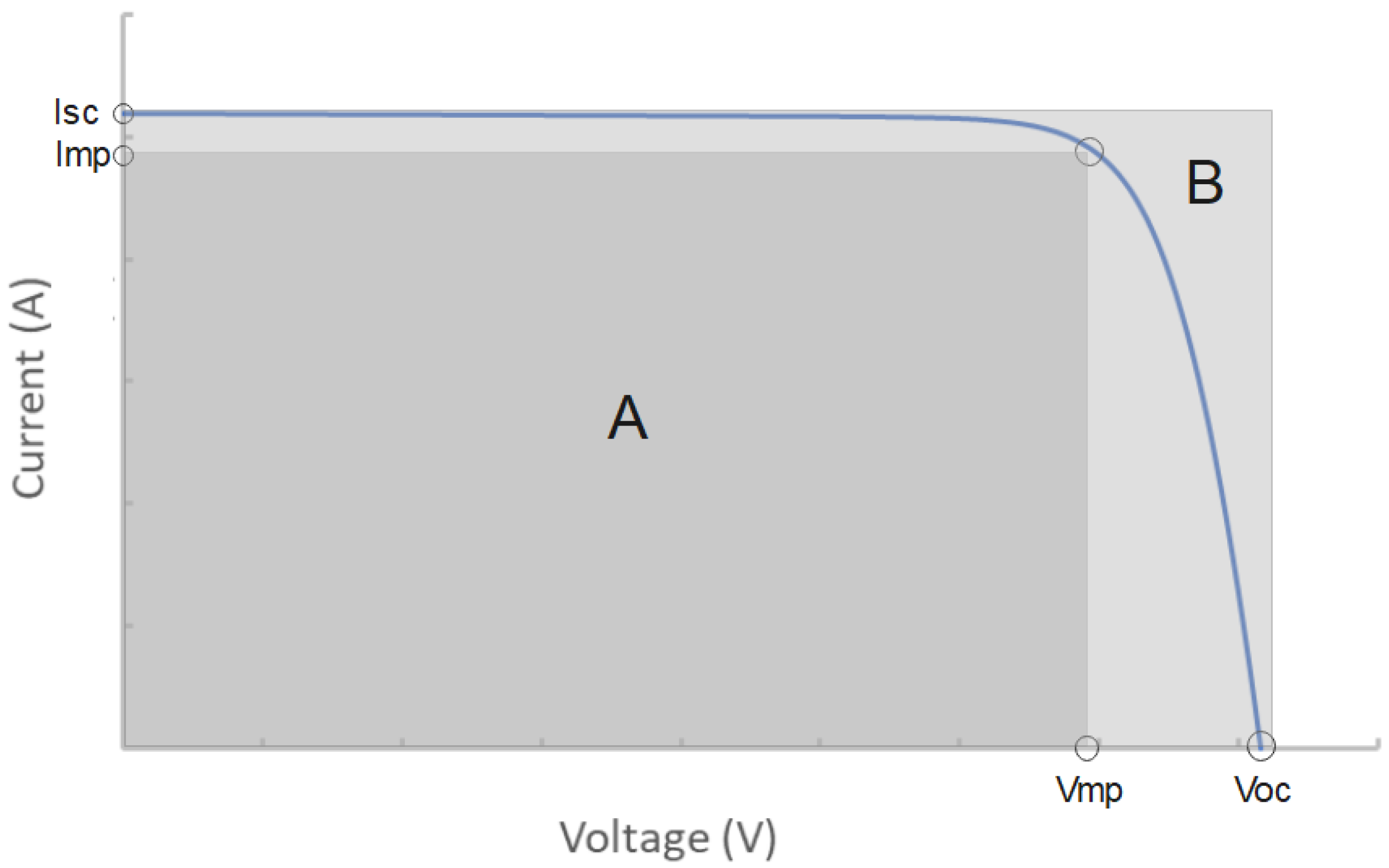
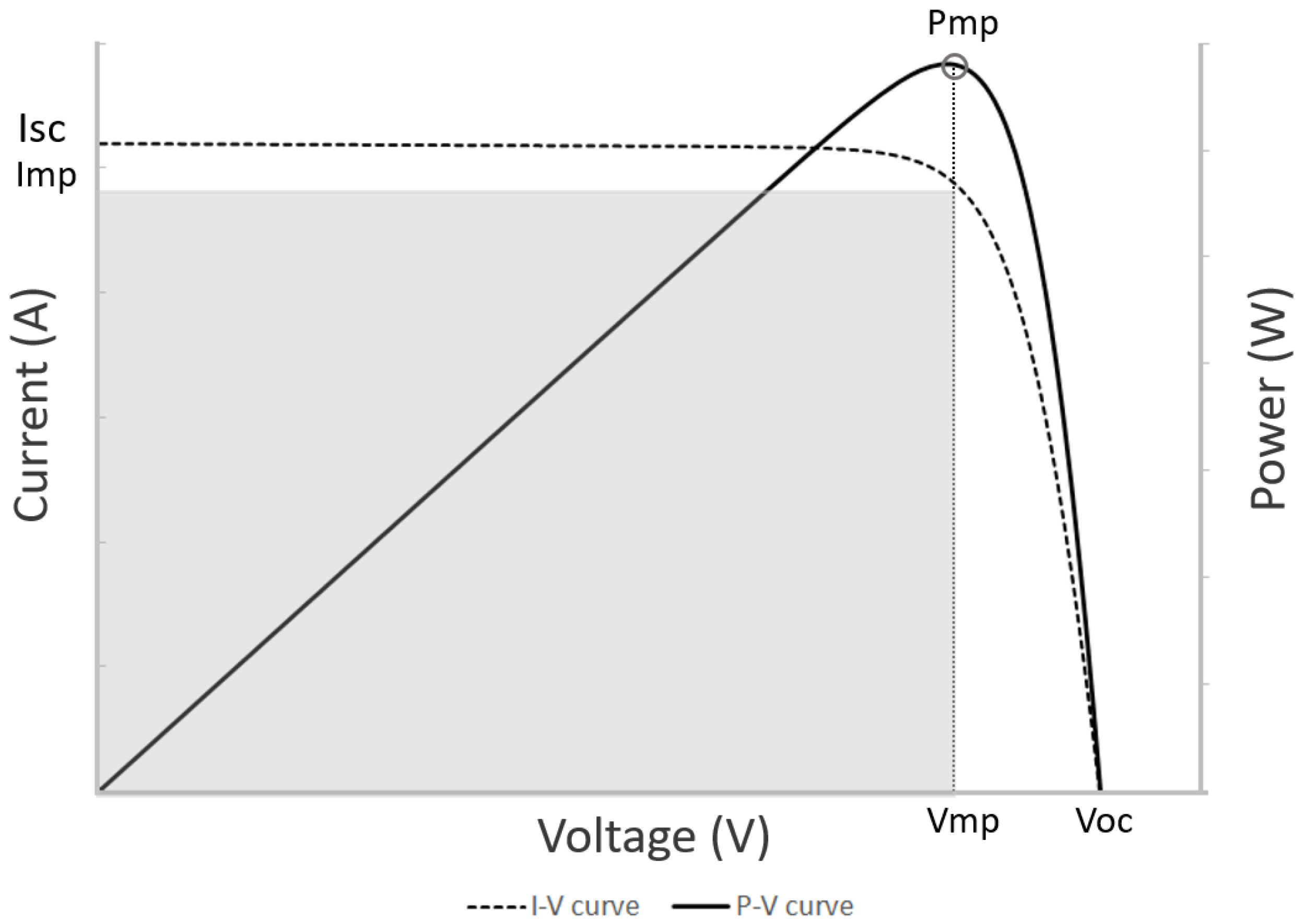
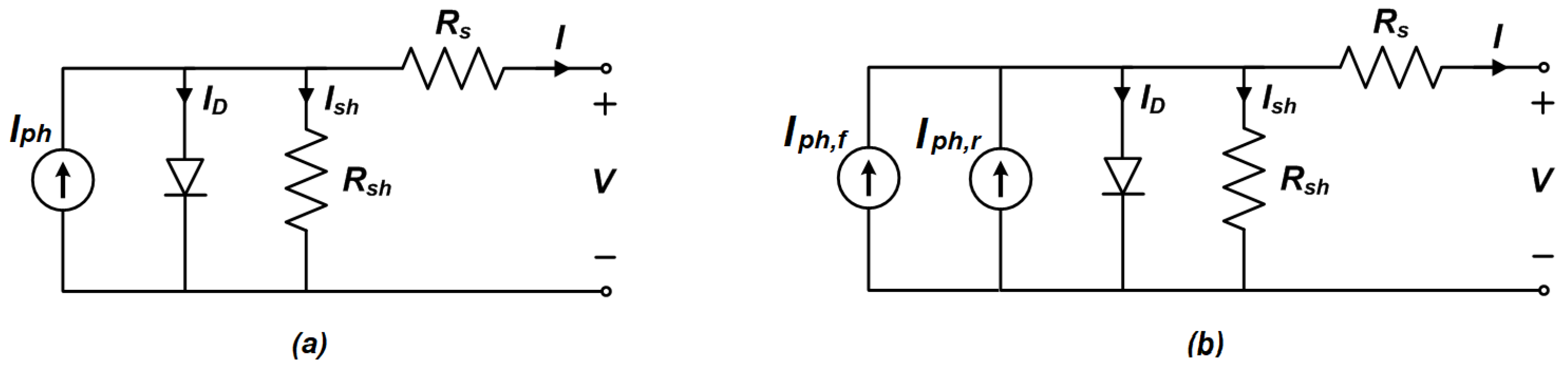
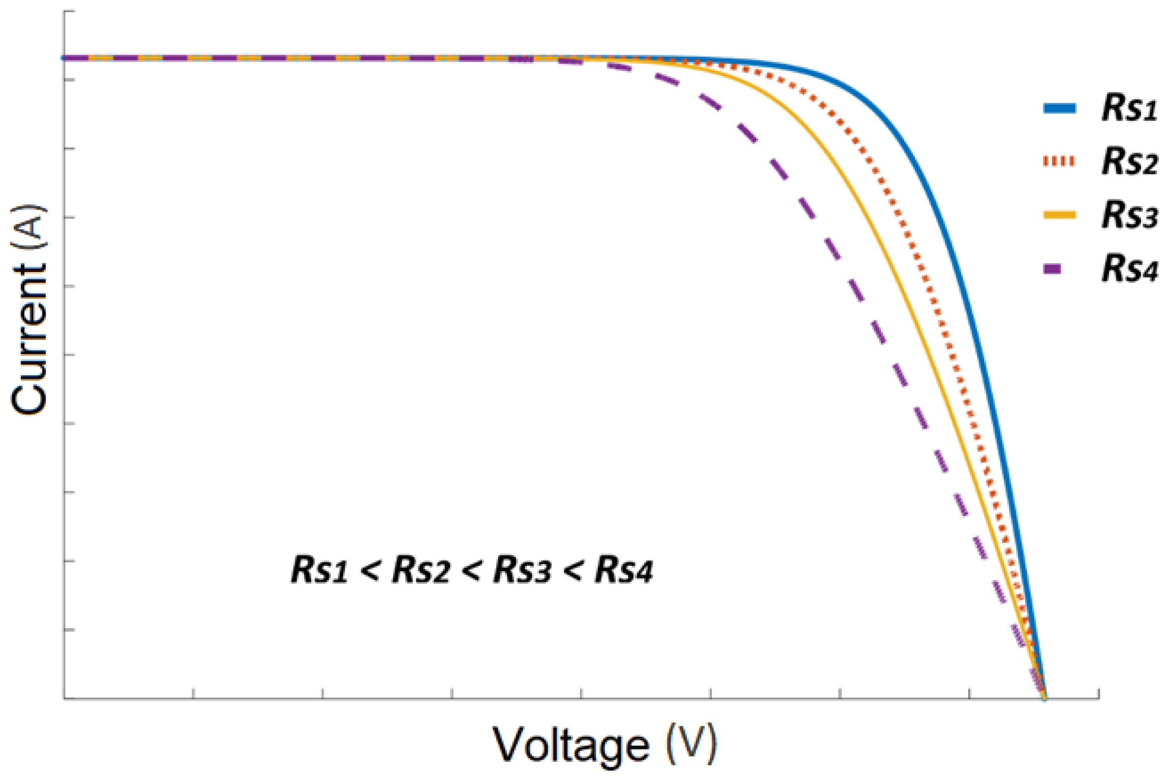
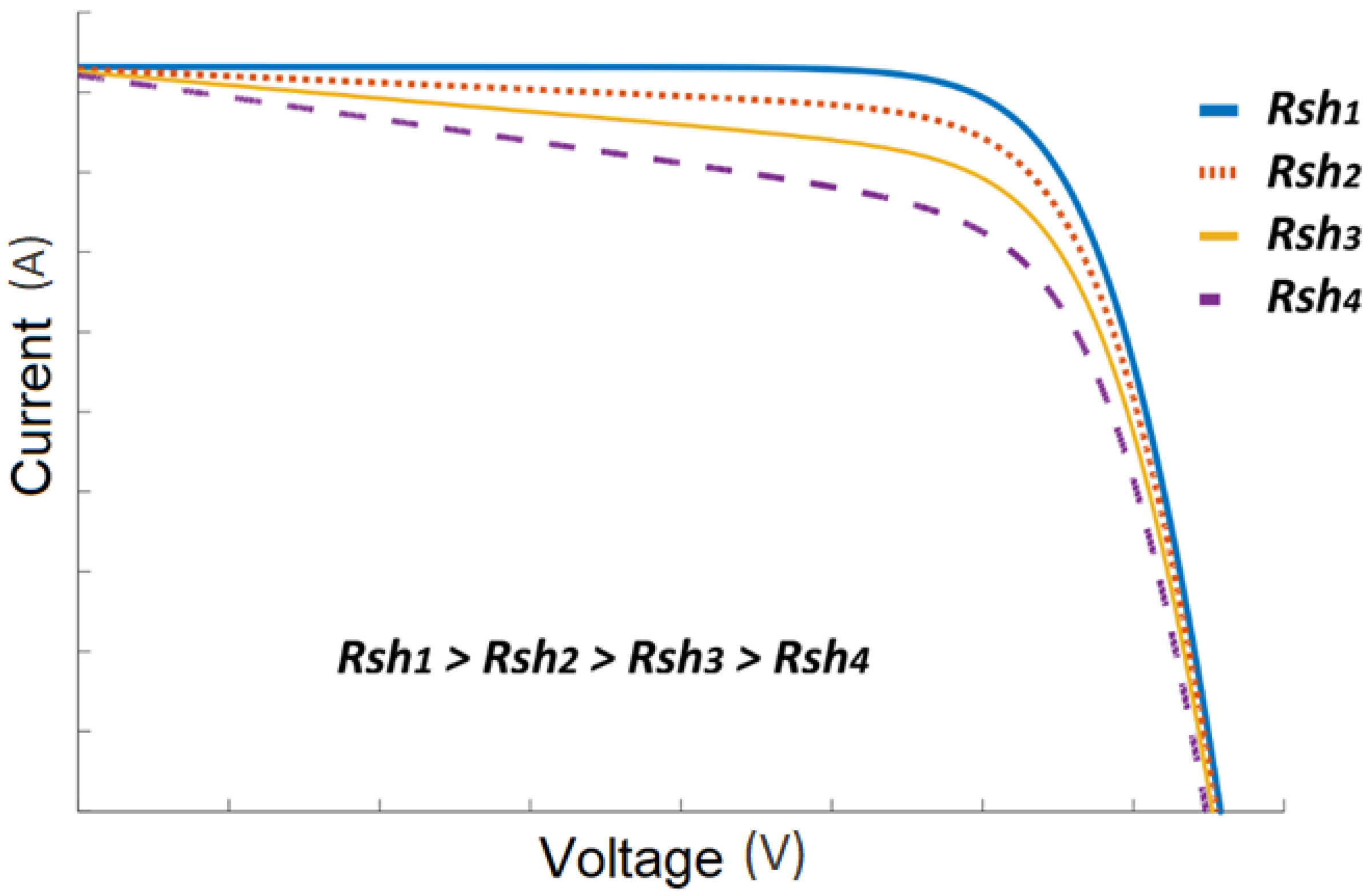
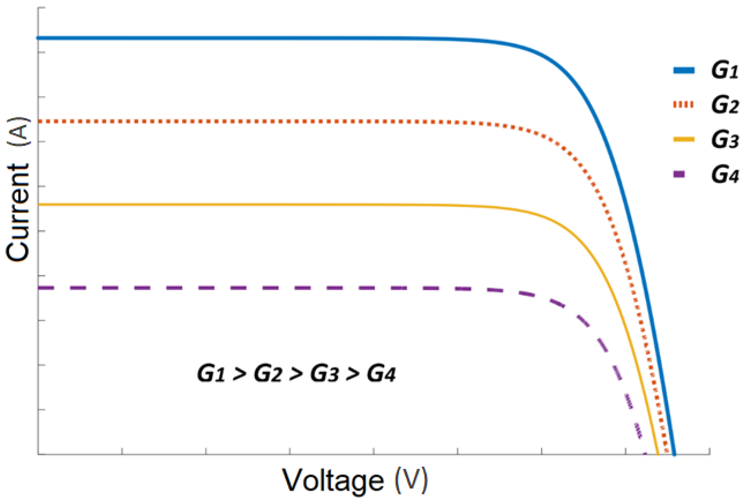
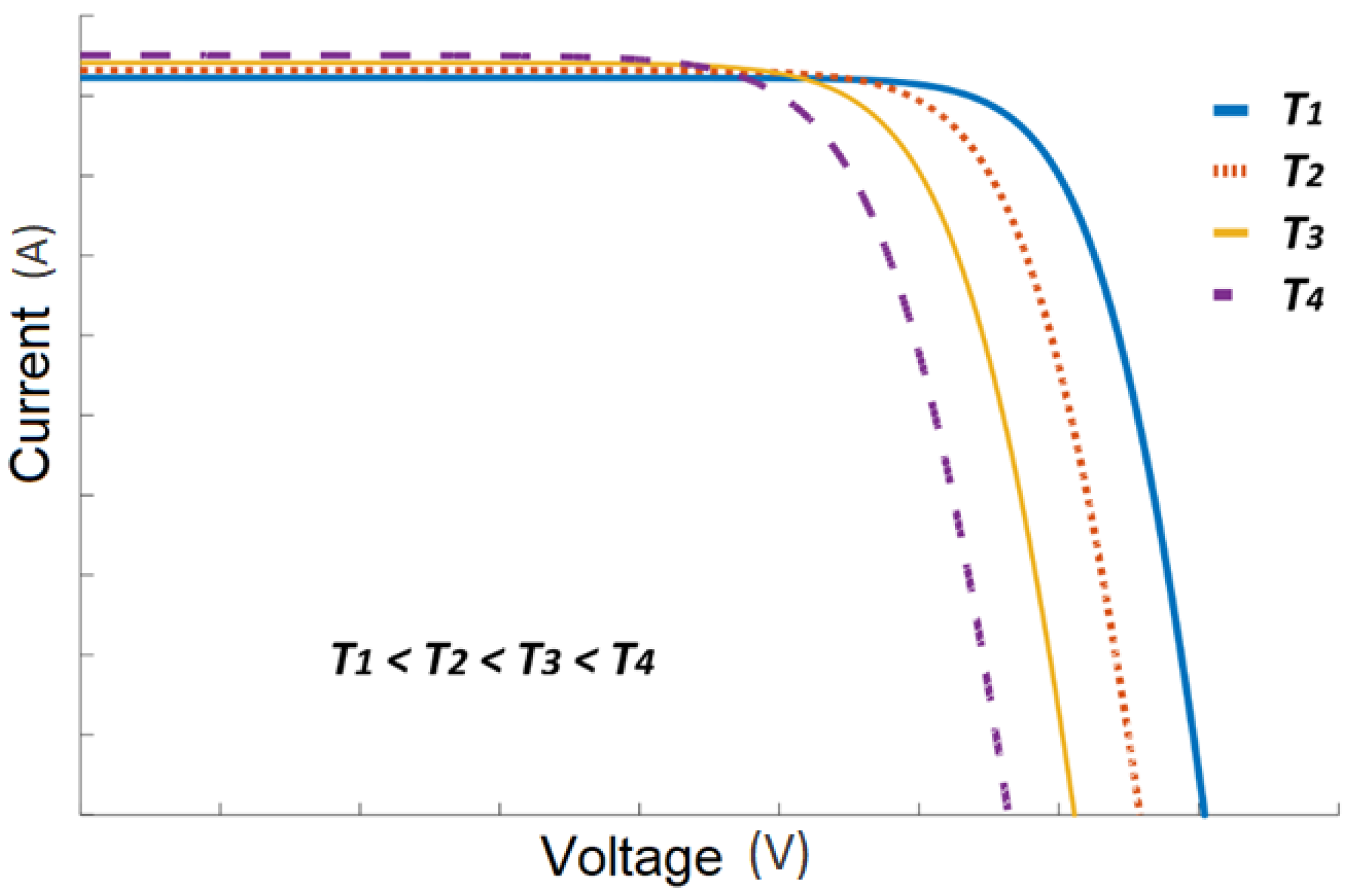
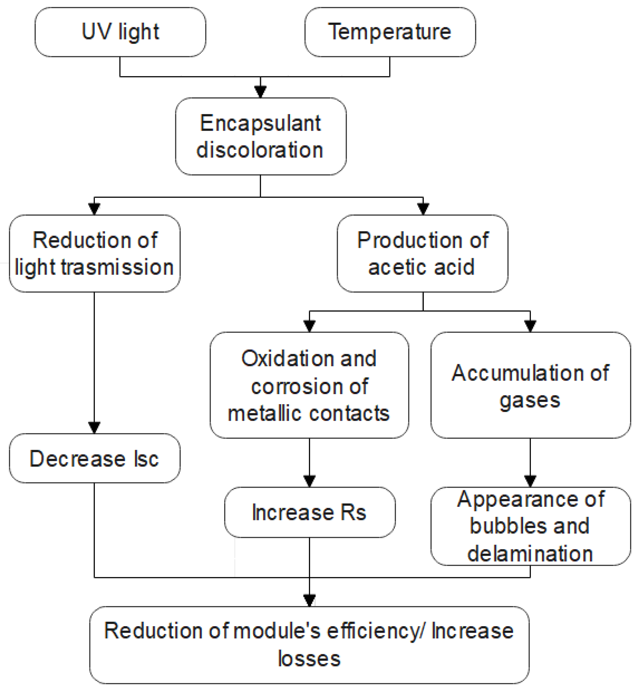
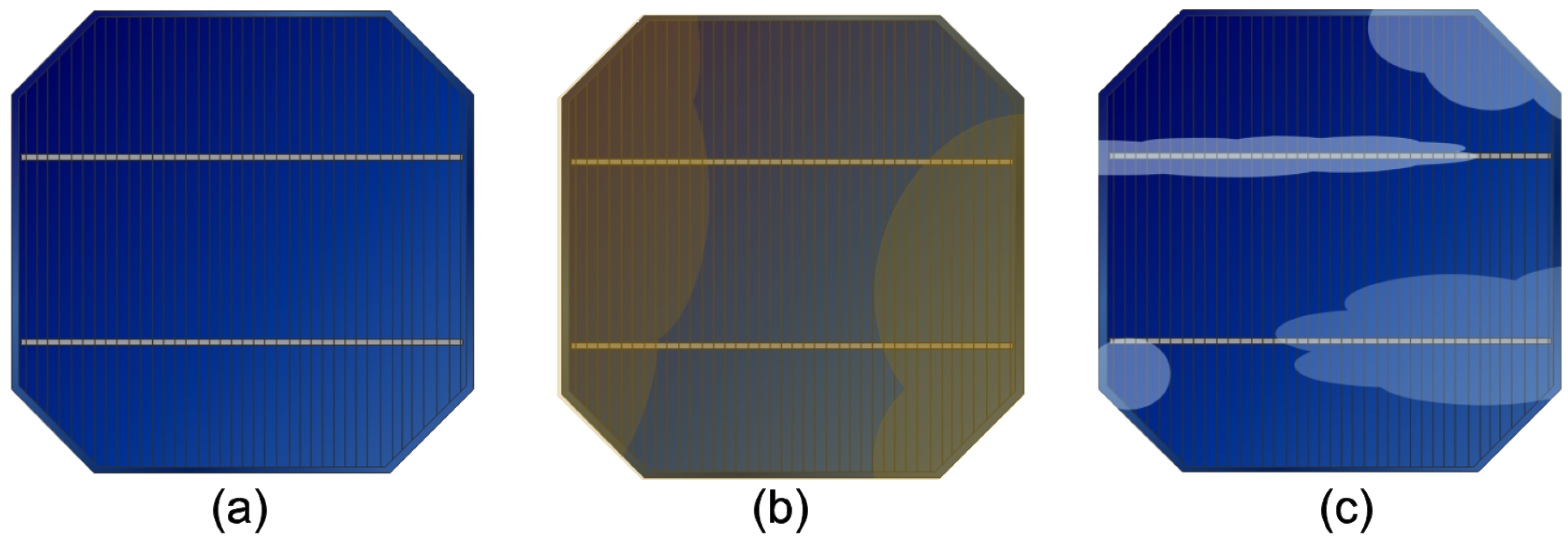
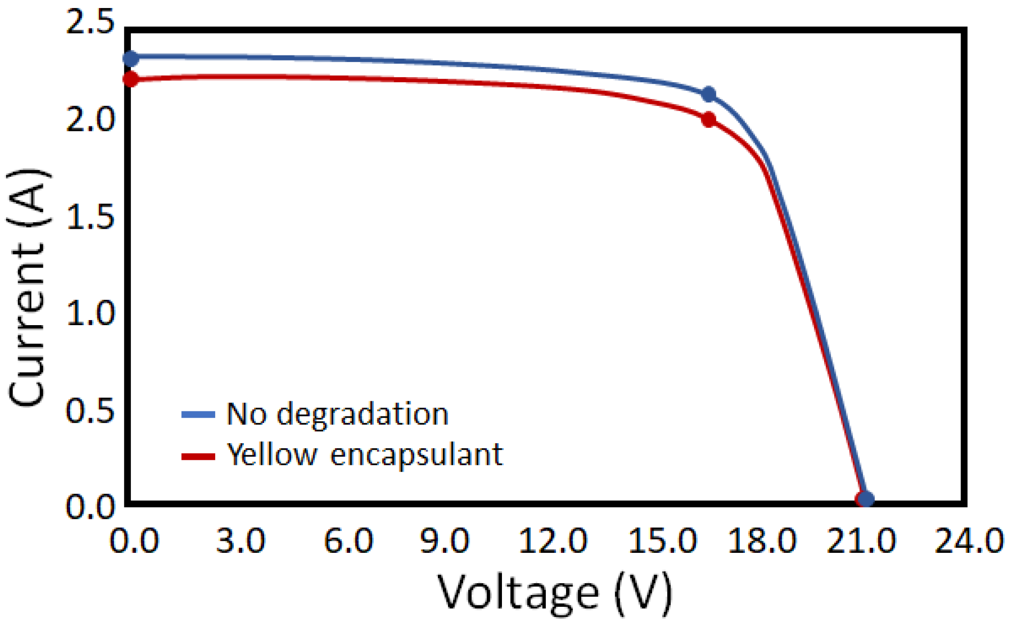
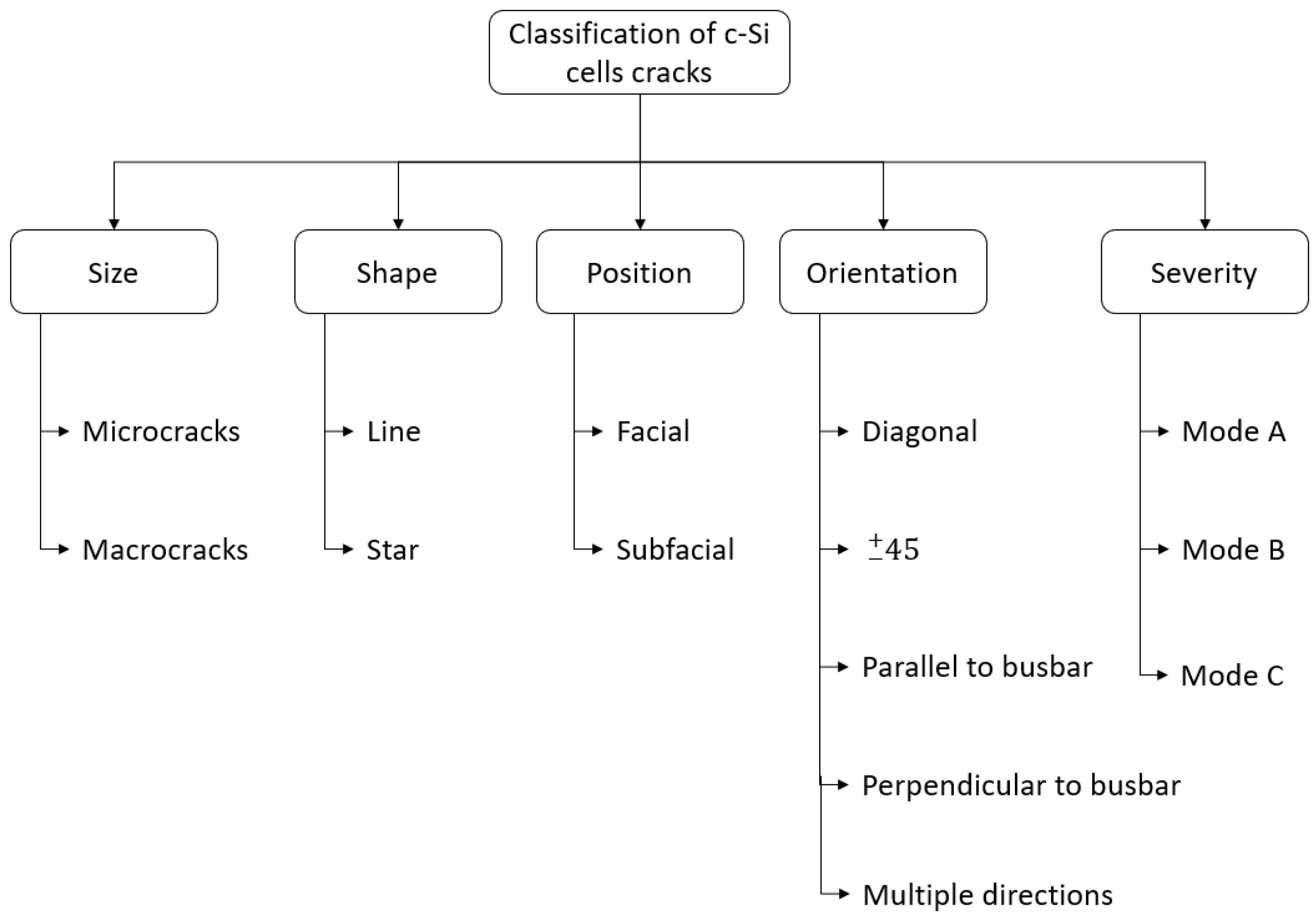
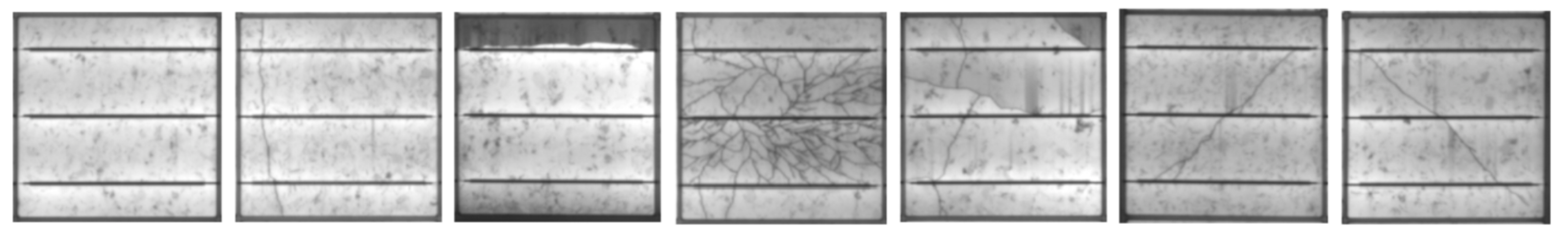
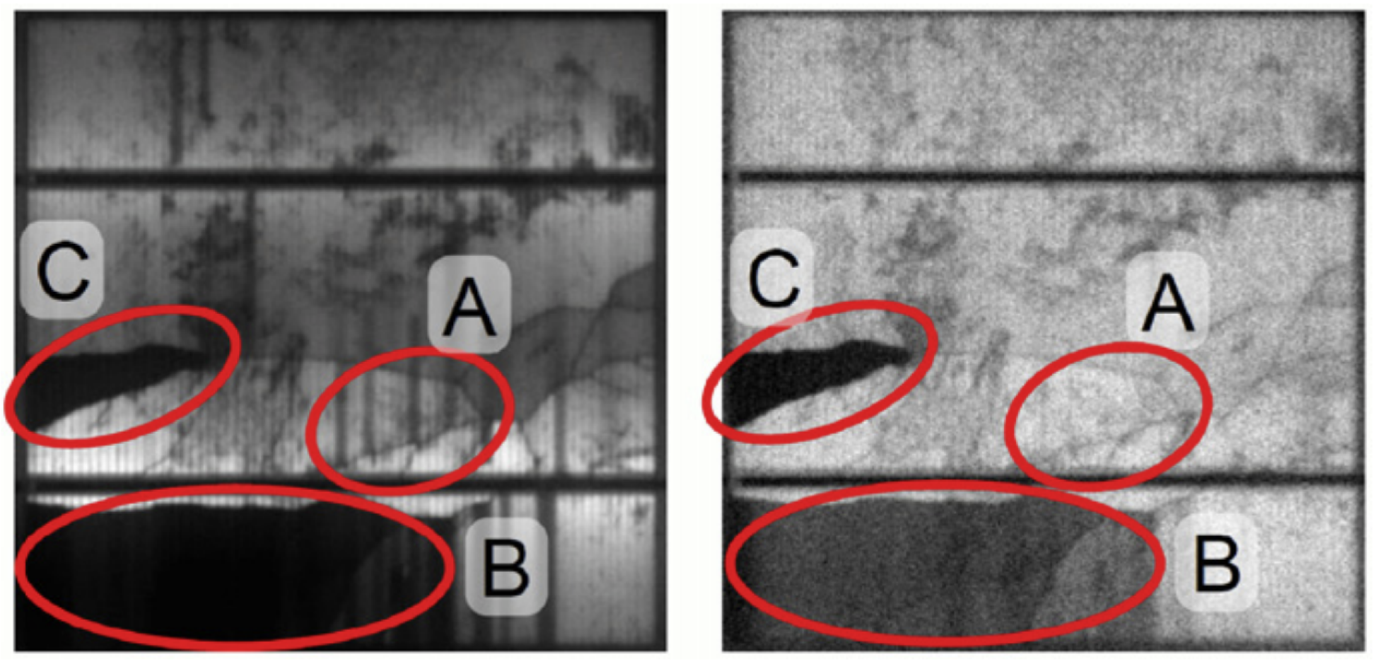
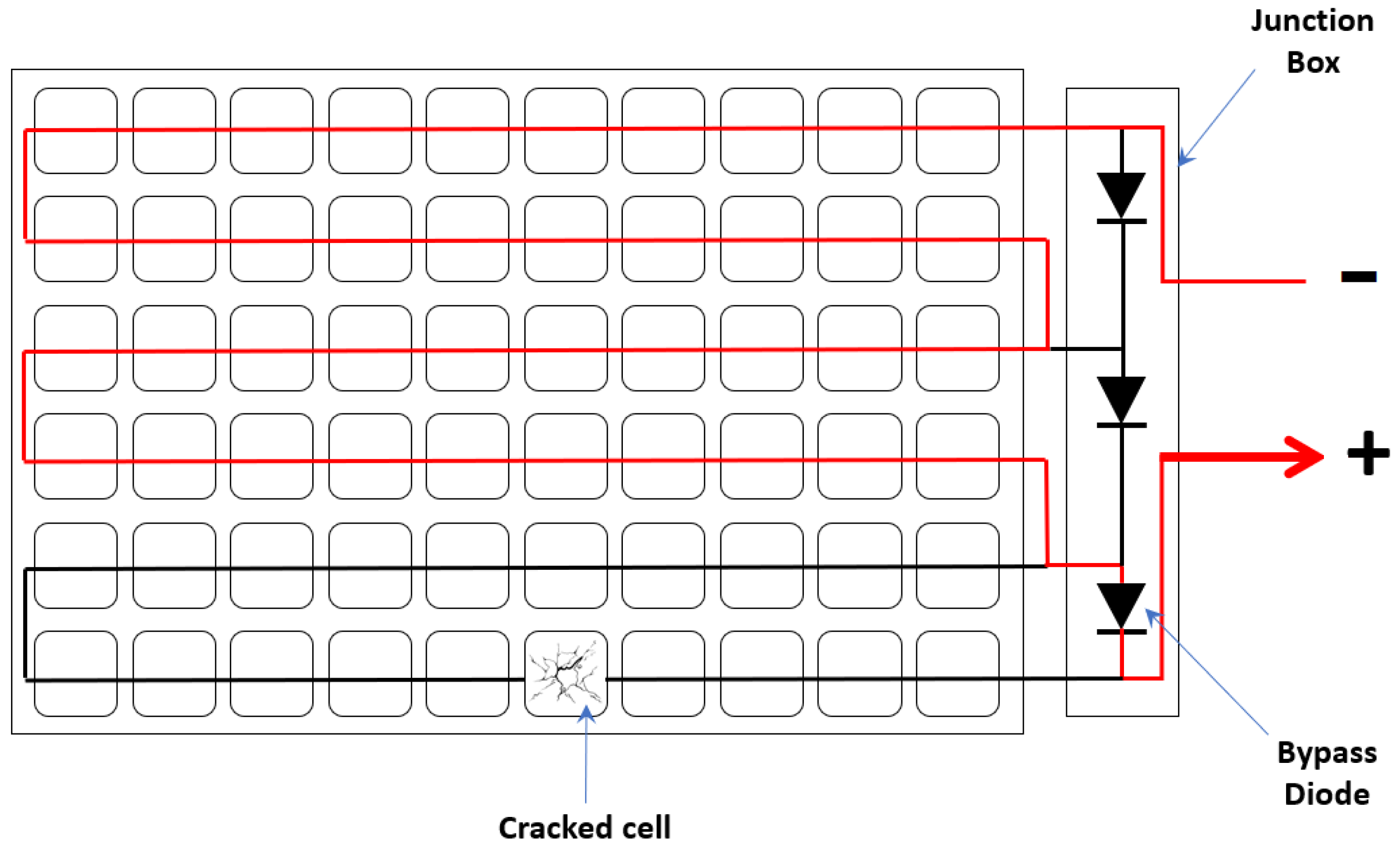
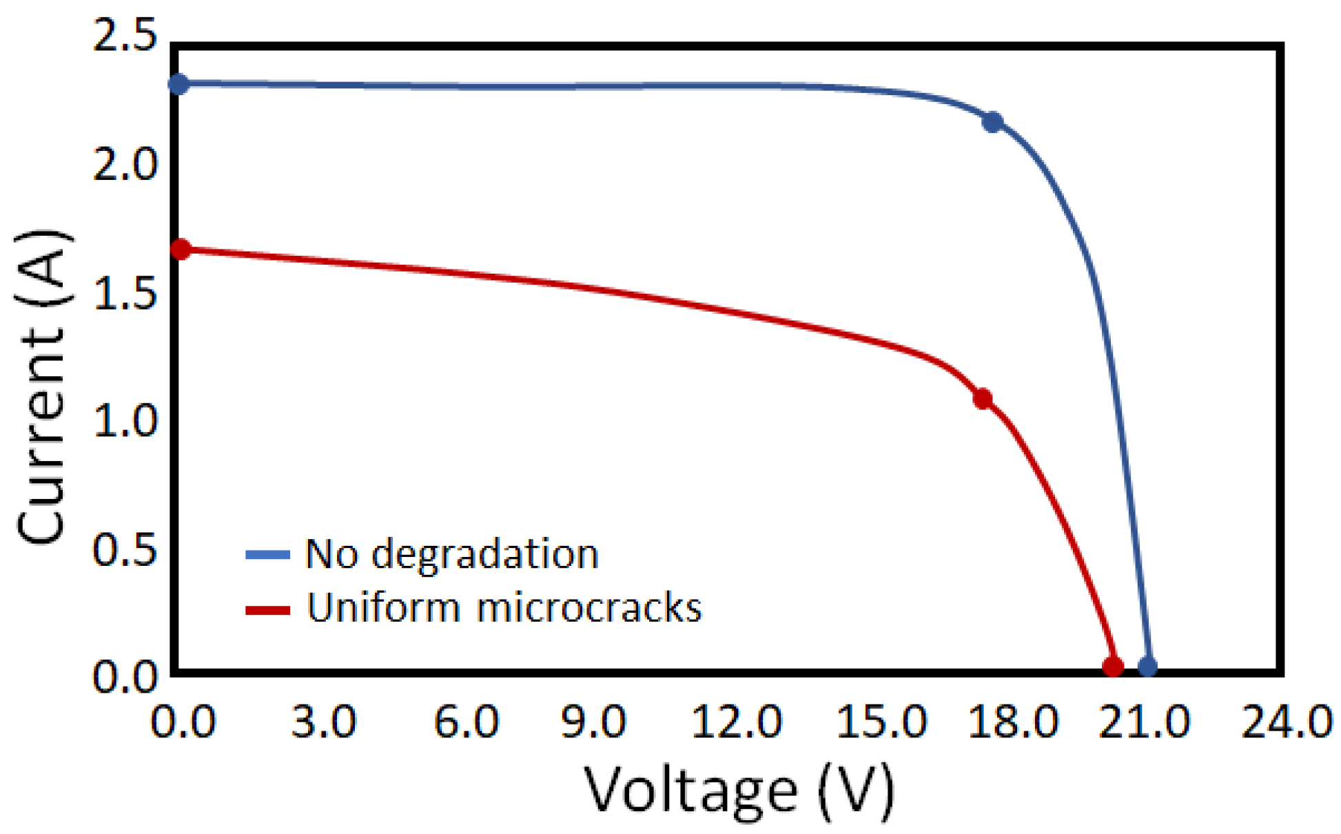
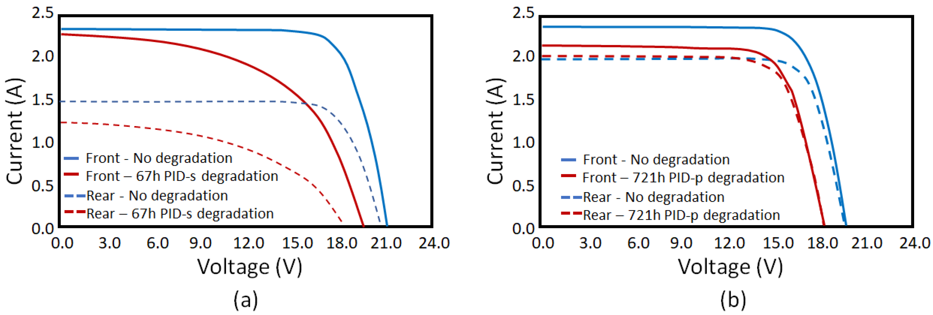
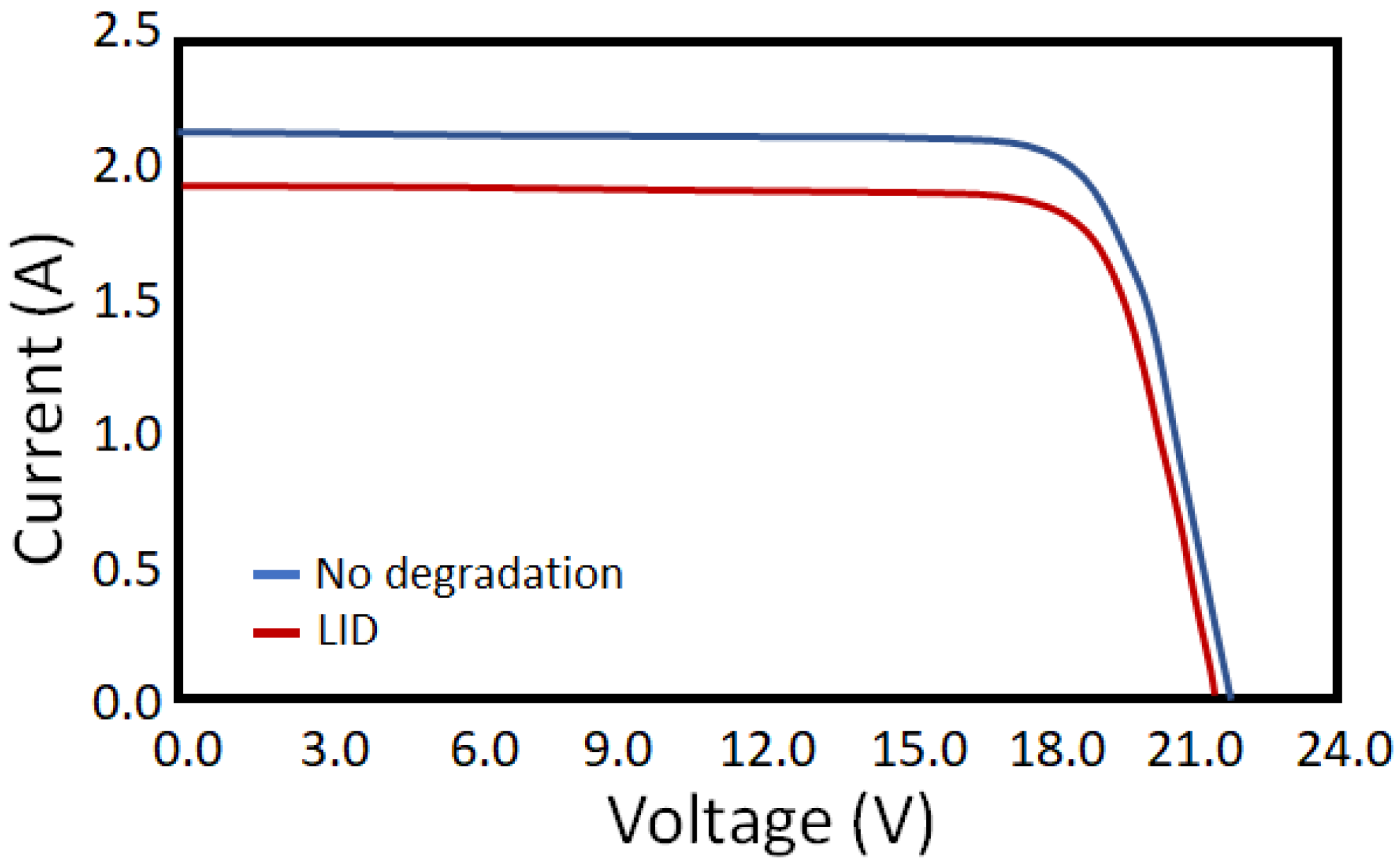
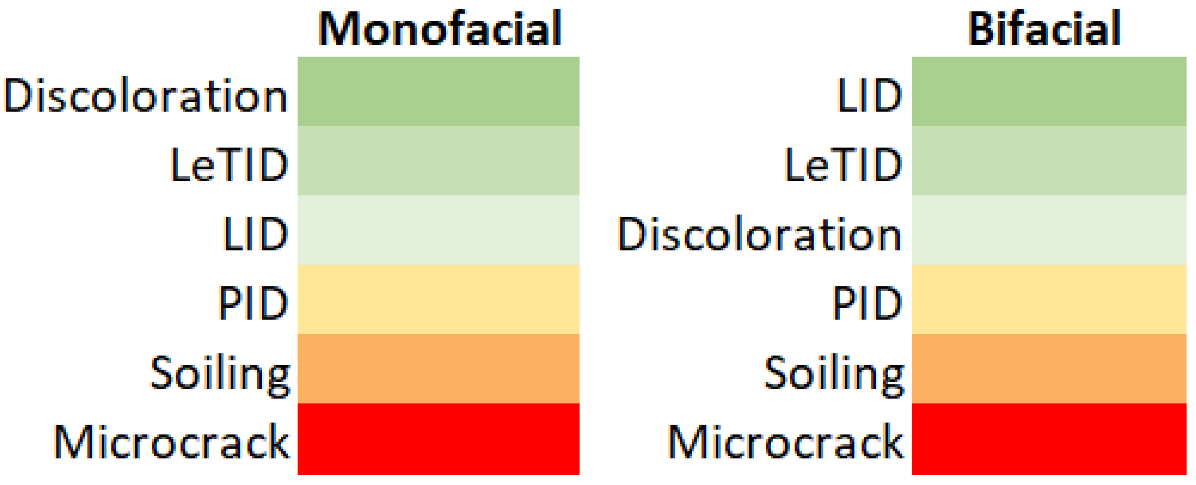
Table 1.
Definitions of the symbols used in Equations (1) and (2).
| Symbol | Definition |
|---|---|
| Efficiency | |
| Fill Factor | |
| Maximum current | |
| Maximum voltage | |
| Short-circuit current | |
| Open-circuit voltage | |
| Maximum power output of the cell | |
| Power received per unity area (W/m) | |
| G | Irradiance incident on the PV cell |
| A | Area of the PV cell |
Table 2.
Definition of the symbols used in Equation (3).
Table 2.
Definition of the symbols used in Equation (3).
| Symbol | Definition |
|---|---|
| I | Output current |
| Diode saturation current | |
| Photogenerated current | |
| V | Voltage at the terminals of the cell/module |
| Series resistance | |
| Shunt resistance | |
| n | Number of cells connected in series |
| a | Diode quality factor |
| k | Boltzmann’s constant ( J/K) |
| T | Ambient temperature (K) |
Table 3.
Causes of microcracks.
| Environmental Causes | Mechanical Stress |
|---|---|
| Thermal cycling | Inappropriate packing |
| Humidity and freezing | Inappropriate transportation |
| Wind load | Unsuitable installation techniques |
| Snow fall/Hail stones |
Table 4.
Power losses due to degradation processes.
| Degradation | Effects on Electrical Characteristics | MPV | BPV | Prevention | |
|---|---|---|---|---|---|
| Irreversible | Encapsulant discoloration and delamination | Reduction of and for discoloration [73] Increase of and reduction of [73] for delamination and oxidation of metal contacts | 0.5% per year [14] 6 to 8% of the nominal 10 to 13% of nominal for complete discoloration. [59] | Glass-glass technology more prone to acetic acid trap and build up increasing the likelihood of bubbles Front side losses 1.3–1.88% per year [16] Rear side losses 0.39–0.78% per year [16] | Replacement of EVA encapsulant by POE and TPO encapsulants [64] |
| Irreversible | Microcracks | Reduction of and “Stepped” I-V curve if the degradation is non-uniform [73] | Directly proportional to the active area | Directly proportional to the active area | Increase number of busbars Re-position the outer busbars closer to the edge of the cell [68,70]. Glass/glass technology [70] |
| Reversible up to 85% loss [74] | PID-s | Degradation < 40%: Increase , and decreases, and not significantly affected. [73,74] Degradation > 40%: Increase , and decreases, and drop significantly [73,74] | Normally up to 30% [74] | 50% power loss— under front side illumination 68% power loss— under rear side illumination [74] | Indoors: Increase module’s temperature[74,79] Reverse bias the cell compared to the grounded frame Increasing refractive index of anti-reflective coat [83] Use of Borosilicate glass or POE or TPO encapsulants [64] |
| PID-p | Drop and but very low effect on . [79] | ||||
| Reversible | LID | Reduction of and [91] | 10% power loss only p-type [88] | p-type Bifacial Multi-Si 1% after 300 kW/m exposure to outdoor light [117] | Expose the cell to illumination and annealing of 1 sun and temperature of 60–300 [93] Preliminary tests at manufacturers according to IEC 61215 [94] |
| Reversible | LeTID | Reduction of and [101]. | Up to 7% power loss p-type and n-type [75]. For solar radiation up to 40 kWh/m, BPV and MPV present similar degradation (1.3%). For higher radiation levels the MPV degradation increases faster than BPV’s [101]. | Bifacial Multi-Si 1.5% after 2000 h (8 years) exposed to hot climate [117] | Expose the degraded cell to elevate temperature and high irradiance [92] |
| Reversible | Soiling | Reduction of and [109] | In desert conditions 0.301% per day [110] | In extreme conditions: 0.236% per year on the front side 0.039% per year on the rear side 0.02% vertical installations [110] | Regular cleaning Electrodynamic screens (EDP) Super hydrophobic plane (SHOP) Super hydrophilic plane (SHIP) |
Publisher’s Note: MDPI stays neutral with regard to jurisdictional claims in published maps and institutional affiliations. |
© 2021 by the authors. Licensee MDPI, Basel, Switzerland. This article is an open access article distributed under the terms and conditions of the Creative Commons Attribution (CC BY) license (https://creativecommons.org/licenses/by/4.0/).
Share and Cite
MDPI and ACS Style
da Silva, M.K.; Gul, M.S.; Chaudhry, H. Review on the Sources of Power Loss in Monofacial and Bifacial Photovoltaic Technologies. Energies 2021, 14, 7935. https://0-doi-org.brum.beds.ac.uk/10.3390/en14237935
AMA Style
da Silva MK, Gul MS, Chaudhry H. Review on the Sources of Power Loss in Monofacial and Bifacial Photovoltaic Technologies. Energies. 2021; 14(23):7935. https://0-doi-org.brum.beds.ac.uk/10.3390/en14237935
Chicago/Turabian Styleda Silva, Michelle Kitayama, Mehreen Saleem Gul, and Hassam Chaudhry. 2021. "Review on the Sources of Power Loss in Monofacial and Bifacial Photovoltaic Technologies" Energies 14, no. 23: 7935. https://0-doi-org.brum.beds.ac.uk/10.3390/en14237935
Note that from the first issue of 2016, this journal uses article numbers instead of page numbers. See further details here.