An Improved Analytical Model for Crosstalk of SiC MOSFET in a Bridge-Arm Configuration


Electromagnetic Theory and New Technology Laboratory, Faculty of Information Technology, Beijing University of Technology, Beijing 100124, China
*
Authors to whom correspondence should be addressed.
Energies 2021, 14(3), 683; https://0-doi-org.brum.beds.ac.uk/10.3390/en14030683
Submission received: 29 December 2020
/
Revised: 22 January 2021
/
Accepted: 26 January 2021
/
Published: 28 January 2021
Abstract
:SiC MOSFETs have an excellent characteristic of high switching speed, which can improve the efficiency and power density of converters significantly. However, the fast switching processes of SiC MOSFETs cause serious crosstalk problems in bridge-arm configurations, which restricts the devices’ performances. This paper presents a detailed and accurate improved crosstalk analytical model, which takes into account the nonlinear capacitances, the parasitic inductances, the reverse recovery characteristics of the anti-parallel diodes, and the nonlinear voltage switching and damping oscillation process. The novelty of the proposed model lies in the fact that under the condition of comprehensively considering all these non-ideal factors of the bridge-arm, the effects of multi-parasitic elements and multi-variables coupling to the crosstalk are hierarchically divided. The parasitic elements and their correlations are described in detail and the direct and indirect variables’ impacts are clearly traced. Thus, according to the different variables switching stages, the influence processes of these parasitic elements and variables can be integrated and a complete equivalent analytical model of the crosstalk process can be derived. The simulation and experiment platforms are established and a series of experimental verifications and comparisons prove that the model can replicate experimental measurements of crosstalk with good accuracy and detail.
1. Introduction
With the advantages of low switching loss, high block-voltage, high switching speed, and high thermal conductivity, SiC MOSFETs increasingly replace traditional silicon-based MOSFETs in high frequency, high efficiency, and high power density applications [1,2,3,4]. However, many kinds of converter topologies are designed based on the bridge-arm structure, the rapid change current and voltage seriously impact the parasitic elements and coupling affect the upper and lower devices, which interfere with the driver loop states and cause wrongly triggered. That is commonly referred to as crosstalk problems [5,6,7]. Especially in the case of SiC MOSFETs are employed in bridge-arm with high frequency, the high current and voltage switching rates significantly increase the amplitude of crosstalk [8]. Furthermore, the gate-source voltage of SiC MOSFETs have lower turn-on threshold voltage and negative breakdown voltage compared with silicon-based MOSFETs [9], and the gate-source parasitic capacitance is relatively smaller [10], these characteristics make the driver loop of SiC MOSFETs more susceptible to the coupling effects. These two factors contradict each other that restrict the SiC MOSFETs’ performances in the bridge-arm, increase the switching loss, and even may cause unintentional turn-on to affect the stability and reliability. Moreover, the crosstalk problem not only exists in common hard-switching conditions but also occurs in the soft-switching bridge-arm [11]. Thus, in order to take full advantage of SiC MOSFETs and avoid the obstacles, crosstalk is a key factor that must be evaluated.
Crosstalk is a phenomenon that involves many parasitic elements of the power loop and driver loop of the bridge-arm and is impacted by different variables during the switching processes. So far, the crosstalk phenomenon has been studied in many works. The most convenient and widely used model is to calculate the peak value of crosstalk, as described in [12,13,14,15,16,17]. It is ascribed to a function of the drain-source voltage switching rate, the input capacitance of the device, and the resistance of the driver loop, as expressed as follows:
Furthermore, in many practical engineering applications, the drain-source voltage switching rates are commonly considered as infinite to obtain the extremum of crosstalk [15,16,17]. The theoretical extremum of crosstalk can be derived from Equation (1) as Vgs_max = VDDCgd/(Cgd + Cgs), where VDD is the drain-source voltage when the SiC MOSFET fully turn-off. In fact, these models have undergone a series of simplifications, only the impacts of driving resistances and constant capacitances of the devices are considered, while the parasitic inductances of the bridge-arm are all ignored, which leads the accuracy cannot be fully guaranteed. More detailed models take into account the influence of other parameters of the bridge-arm, the models in Ref. [18] and Ref. [19] consider the influences of parasitic inductances, which indicate that the switching current of the bridge-arm generates an induced voltage on the common source parasitic inductance, it is superimposed on the driver loop and affects the crosstalk. Literature [20] established a detailed crosstalk equivalent analytical model that includes all the parasitic inductances of the power loop and the driver loop. The time-domain response of the crosstalk can be obtained, which is summarized as a fourth-order differential equation. However, the model still relies on the given drain-source voltage switching rate as the input source, it is not been further evaluated in detail. Moreover, since the existence of the parasitic inductances in the whole bridge-arm, the reverse recovery current of the anti-parallel diode during the turn-on process also impacts the crosstalk voltage [21,22], and in Ref. [23], the effects of the reverse recovery current on crosstalk are analyzed in detail. More and more complete considerations of the parasitic elements improve the accuracy of the crosstalk analysis but greatly increases the complexity of the model establishment. In additon, the current studies mainly focus on the coupling relationship between the crosstalk and the parasitic elements, while the analysis of the variable responses as the influence sources, caused by the bridge-arm switching processes, to the crosstalk is relatively simple.
Another critical aspect is the precise description of parasitic elements and the correlative variables, it is ultimately related to the accuracy of the crosstalk response. It is well known that the interelectrode capacitances of SiC MOSFETs have nonlinear characteristics, which should be accurately described during the voltage switching processes [24]. Although the effect of nonlinear capacitances on the switching processes of SiC MOSFETs has been thoroughly studied [21,25,26,27,28], its impacts have been not enough detailed analysis for the crosstalk, which include the effects on the switching speed of the active-controlled device and the influence on the characteristics of crosstalk response circuits. The variable responses of the bridge-arm are commonly the main influence sources of the crosstalk. Elbanhawy et al. proposed a method that the voltage switching rate is regarded as a constant value [15,16,17], it could cause calculation errors for crosstalk from the source. In fact, the voltage switching is a nonlinear change process [20], Ref. [20] proposes a method of using experimental measurement switching rates to facilitate the calculation accuracy, but it cannot play a role in predicting the crosstalk fundamentally and explain how the nonlinear voltage switching rate influences the response. During the whole switching process of the bridge-arm, the main variables are switched by stages (voltage switching stage, current switching stage, and the reverse recovery process of the anti-parallel diode). In order to get the entire crosstalk response, the coupling effects of these variables and the coupling parasitic elements are different, which should be discussed separately and precisely [21,24]. In addition, some variable responses have overlapping situations, such as the reverse recovery current drop process coincides with the voltage rising stage in the turn-on process [8,29], which increases the complexity of the analysis. Moreover, due to the inertial effect of the parasitic elements, there are oscillation responses of the voltage and current after the full switching process of the bridge-arm [30,31,32,33], which are also coupled to the driver loop and impact the crosstalk. To sum up, although these special characteristics and response processes greatly cumber the model design, they ultimately related to the accuracy of the crosstalk response. However, there is no complete model that can describe the crosstalk process correlates with these parasitic elements and the key variable responses of the bridge-arm particularly and comprehensively.
This paper presents a detailed and accurate analytical model of crosstalk for SiC MOSFETs applied in the bridge-arm configuration. In view of the complex coupling characteristics of multi-parasitic elements and multi-variables in the crosstalk response process, the influencing factors are summarized first. Crucially, the nonlinear characteristics of the interelectrode capacitances, the reverse recovery characteristics of the anti-parallel diodes, the parasitic inductances of the power loop, and the nonlinear voltage switching and damping oscillation process are analyzed in detail to ensure accuracy from the source. According to the switching processes of the bridge-arm, the correlation of the variables and parasitic elements with crosstalk in each stage are distinguished and the influence mechanisms behind these parameters are traced clearly. On this basis, a detailed analytical model of crosstalk is established, the source impact variables and the critical parasitic elements are all considered and combined, their direct or indirect coupling effects to the crosstalk in different switching stages are clarified. The equivalent circuits of the switching stages are established and calculation procedures are derived hierarchically. In the most critical voltage switching stages, the multitude of impact factors can be linked to the response of the drain current, it plays a key role in the impacts of crosstalk from the power loop to the driver loop, and then the crosstalk can be further evaluated with this unique direct impact source. A double pulse test platform composed of 600 V/36 A SiC MOSFETs is set up and a series of experimental results are provided to verify the correctness and accuracy of the proposed analytical model. Further, the simulation calculations and experimental results are compared with the calculation results in [17,24], and the theoretical extremums, the results show that the proposed model can describe crosstalk response in more detail and accuracy.
2. Analysis of Crosstalk Response Processes and Related Factors
A double-pulse test based on a bridge-arm configuration is a simple and effective way to analyze the crosstalk process. In this paper, a double-pulse test circuit is established to explain the crosstalk phenomenon. The equivalent circuit model is shown in Figure 1. The DC input bus voltage VDD is modeled as a constant voltage source, and the output current ILOAD is set as a constant current source. The upper SiC MOSFET, QH, is the active-controlled device, which works in the normal turn-on/off states, the lower SiC MOSFET QL is set at a constant turn-off state, which is used to observe the VgsL crosstalk response. During the QH cut-off period, the load current ILOAD flows through the antiparallel freewheeling diode of QL, DbL.
The parasitic elements and of SiC MOSFETs devices and the bridge-arm circuits should be considered as comprehensively as possible to ensure accuracy. In practice, there are usually parasitic inductances distributed in the power loop, which are summarized as LLOOP. The parasitic elements of the SiC MOSFETs need to consider the internal of the device package and the external circuit traces, as shown in Figure 1. Taking QL as an example, the internal parasitic elements include interelectrode capacitances CgsL, CgdL, CdsL, where they have nonlinear characteristics, parasitic inductances of gate, drain, and source, LgL_in, LsL_in, and LdL_in, internal gate driver resistance RgL_in, and the antiparallel freewheeling diode DBL, where it has reverse recovery characteristic. The external parasitic elements are the stray inductances of the electrode pins and the circuit traces connected with the gate, source, and drain, which are represented by LgH_ex, LdH_ex, and LsH_ex, respectively. Generally, there is an external driver resistance RgL_ex in the driver loop to regulate the switching speed. In order to facilitate the analysis, denoting LgH = LgH_ex + LgH_in, LdH = LdH_ex + LdH_in, LsH = LsH_ex + LsH_in as the total gate, drain, and source inductances of QL, and RgL = RgH_ex + RgH_in as the total gate resistance of QL. QH has the same structure.
At present, most discrete SiC MOSFET commercial products have two package structures, non-Kelvin package and Kelvin package. For non-Kelvin package device (such as TO-247-3), the parasitic inductance of the source should be emphasized, it is contained in the power loop and the driver loop, which makes the driver loop more vulnerable to the coupling effect of the current variation of the power loop, as is shown in Figure 2a. While the source of the Kelvin package device (such as TO-247-4) is separated for the driver loop and the power loop, which could get rid of this drawback, as shown in Figure 2b. However, the internal common source parasitic inductance cannot be completely ignored, the coupling impacts from the power loop still exist [24]. Moreover, non-Kelvin package SiC MOSFETs are widely adopted in engineering applications. Thus, the crosstalk with non-Kelvin package SiC MOSFETs is mainly discussed in this paper. The impacts of common source parasitic inductance are greater than that of the Kelvin package devices, and the analysis processes are more complicated due to the superposition influences of the power loop. This analysis method can also be simplified and transplanted to similar Kelvin packaged discrete devices and modules.
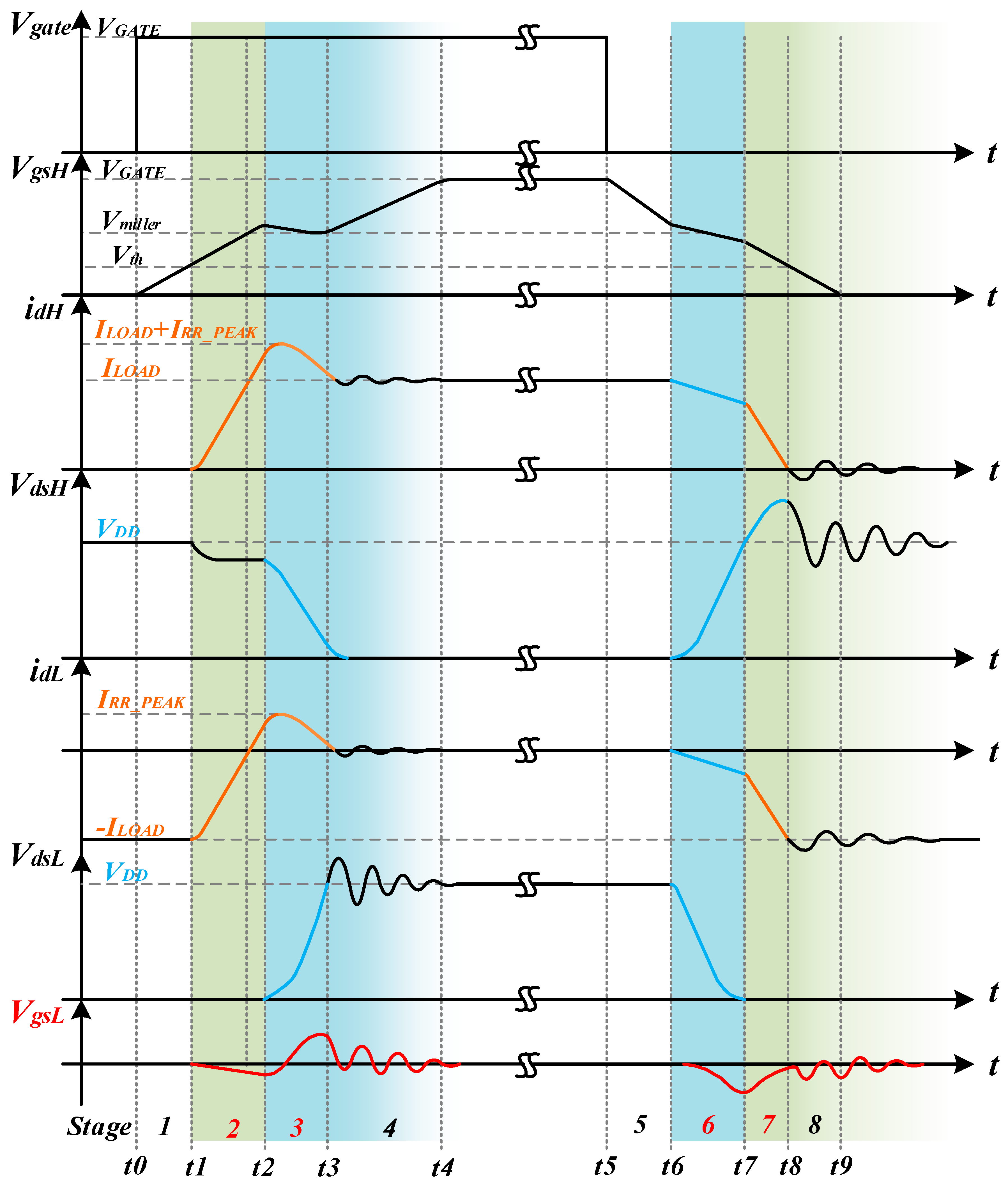
In the bridge-arm configuration, the parasitic elements and their characteristics not only directly determine the response characteristics of the crosstalk voltage, but also affects the voltage and current switching process of the bridge-arm, which indirectly determine the impact sources to the crosstalk. Therefore, all these parasitic elements and their influence on the whole switching process should be integrally considered. At present, the operation characteristics and switching processes modeling of various types of power devices have been thoroughly studied in many researches. For a non-linear variation switching process of the device, the piecewise linear model is the most convenient and widely used analytical model [34,35,36]. Based on the piecewise linear analytical model for the switching devices, the analysis can be further related to the influence on the switching processes and crosstalk responses of bridge-arm configuration. From the perspective of crosstalk voltage, the key parameters and variables associated with crosstalk in each stage are further extracted. Thus, a thorough analysis of the influences of parasitic elements and switching variables on crosstalk and switching variables is presented. Figure 3 illustrates a typical double-pulse test turn-on and turn-off qualitative switching waveforms. Among them, Stage 2 and Stage 7 are the current switching stages of the turn-on and turn-off process, respectively. Stage 3 and Stage 6 are the voltage switching stages of the turn-on and turn-off process, respectively. The fluctuation of VgsL is displayed in red in Figure 3.
The current and voltage switching in the power loop of the bridge-arm cause two key effects that affect the crosstalk. The first one is the rapid current switching generates an induced voltage on the common source parasitic inductance, LsL, which is superimposed in the driver loop. The second one is the voltage switching causes a displacement current of the gate-drain capacitance, CgdL, which forms a circuit through the driver loop. Both of them are directly related factors to the responses of VgsL.
More specifically, in the turn-on process of QH, the supply current of ILOAD transfers from DBL to the channel of QH first, which corresponds to Stage 2 in Figure 3. The freewheeling current flowing through DBL decreases rapidly. Due to the reverse recovery characteristics, after the freewheeling current drops to zero, the minority carriers of DBL need to be elicited first, which causes a positive reverse recovery current increase. Thereafter, DBL turns to the reverse-biased state and the blocking voltage starts to build up. During the whole process before the formation of the depletion layer of DBL, there is no reverse-blocking capability and VdsL does not increase. Thus, only the induced voltage of LsL is coupled to the driver loop of QL in this stage. The equivalent circuit of this stage is shown in Figure 4a.
The equations of the driver loop of this stage can be expressed as
During Stage 3, the drain-source voltage of QL is built up (the blocking voltage of DBL increases). The gate-drain capacitance CgdL is charged, the charging current flows through CgsL and the driver loop of QL, which causes a positive crosstalk voltage of VgsL. In addition, it must be noted that the power loop maintains the reverse recovery current at the end of the previous stage, which approaches its peak value and keeps the rising rate. It can be considered as the initial conditions during the increase process of VdsL. With the increase of VdsL, the current charging the parasitic capacitances of QL (CgdL, CdsL, and CgsL), idL, decreases gradually. The equivalent circuit of this stage is shown in Figure 4b. The induced voltage on LsL becomes negative, which also causes a positive impact on VgsL. The circuit equations are established as
where VDSL is the voltage between the phase node and ground.
When VdsH reaches the on-state voltage, QH is completely cut-off. VdsL rises to VDD and keeps the rising rate at t4, then it starts oscillating due to the parasitic inductances of the power loop and the parasitic capacitances of QL. The oscillations of voltage and current are coupled to the driver loop through CgdL and LsL, which further cause fluctuations on crosstalk, as shown waveforms after t3 in Figure 3. The equivalent circuit is the same as Figure 4b.
In the turn-off process of QH, its channel resistance starts to increase first, which corresponds to Stage 6 in Figure 3. VdsH starts to rise and VdsL decreases, DBL withstands a negative voltage and the current does not yet switch in this stage. However, the charging and discharging of the parasitic capacitances lead part of the bridge-arm current transferred to maintain the constant of the load current. The initial states of the parasitic capacitances discharge current of QL are zero, and the equivalent circuit is shown in Figure 5a. Same as Stage 3 in the turn-on process, the voltage and current variations all affect the crosstalk response, but the variables’ directions are opposite. VgsL has a negative fluctuation. When VdsL drops to the forward turn-on voltage of DBL, the voltage switching is completed and the current begins to divert from the channel of QH to DBL. A negative induced voltage on LsL is superimposed on the diver loop of QL, which causes a positive fluctuation impact on VgsL. as shown the Stage 7 in Figure 3. The equivalent circuit is shown in Figure 5b. the expressions of these two stages are the same as the turn-on stages, Stage 3 and Stage 2, respectively.
Based on the analyses above, it can be seen that the response of VgsL in different stages corresponds to different variables of the bridge-arm and correlate with many parasitic elements, which makes the modeling cumbersome. Especially in the voltage switching processes, the coupling of the two influence paths associates five independent state variables, the crosstalk response of VgsL is simplified to a fourth-order differential equation, it is difficult to derive the time domain solutions. Moreover, compared with Equation (4) in [24], the order of VgsL response is significantly increased, which is due to the influence of parasitic inductances are taken into account.
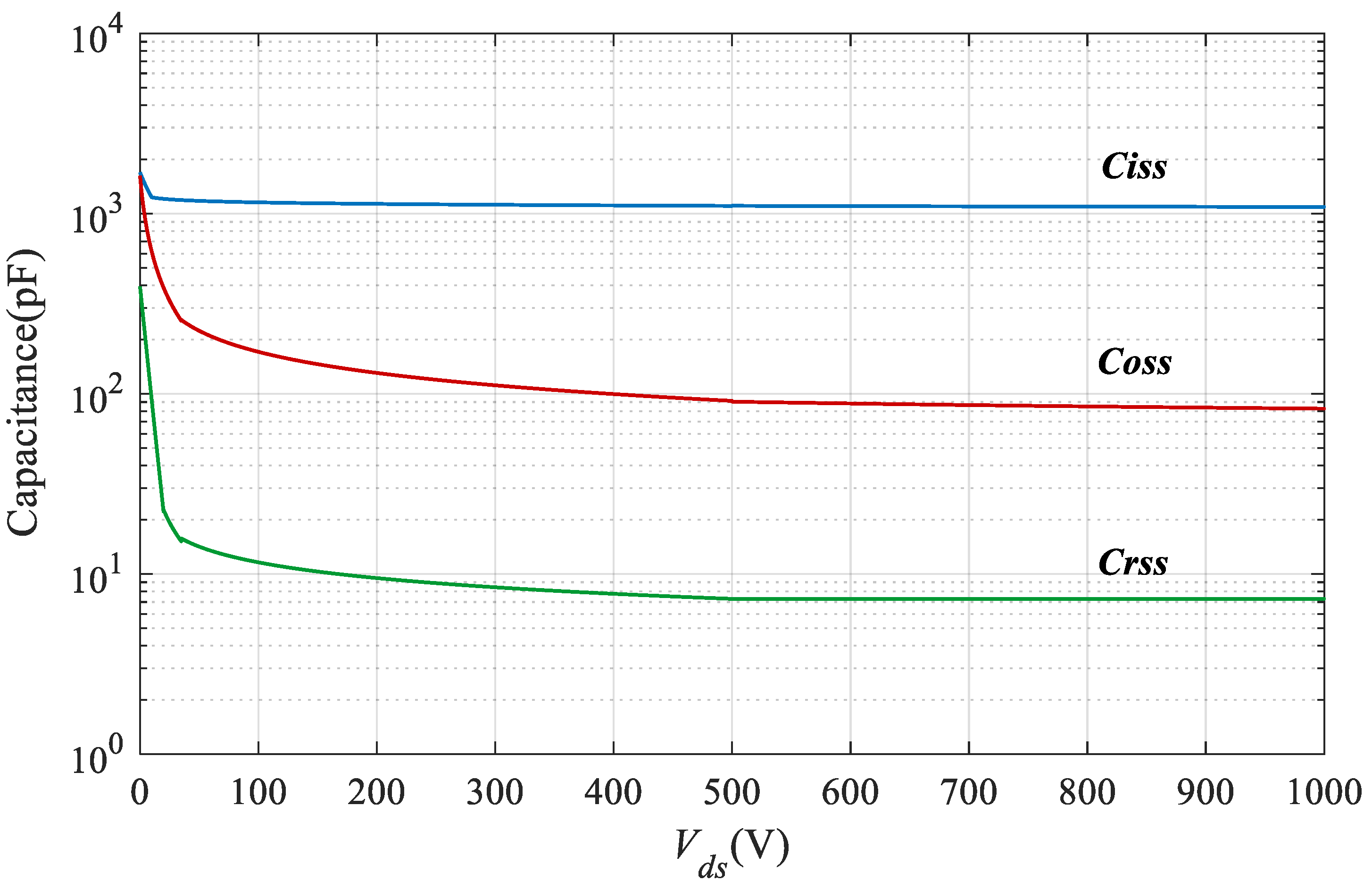
Further, there are several special parameter characteristics of SiC MOSFETs in the above-mentioned switching processes also affect the accuracy of crosstalk that must be carefully considered. SiC MOSFETs have smaller parasitic capacitances than silicon-based devices, and their values are nonlinear versus the drain-source voltage. For the SiC MOSFETs with type CMD080120D, the nonlinear curves are shown in Figure 6. It can be found that especially the nonlinear variation of reverse capacitance Crss (Cgd), it decreases nearly a hundredfold with the increase of VdsL. This variation has an obvious influence on the characteristic of the Cgd displacement current loop, which directly associates with the crosstalk response according to the Equations (5)–(8). Literature [24] also clearly verified the impact of the nonlinear characteristics of CgdL on the accuracy of the crosstalk response.
Moreover, the nonlinear variation of the parasitic capacitances of QH also affects the voltage switching rate. According to the literature [20,24,37], the switching rate of VdsH is determined by the driving current igH and the CgdH. Due to the restriction of the voltage dynamic equilibrium of the whole bridge-arm, the response of VdsL presents a nonlinear variation process. As one of the input sources of the crosstalk in Stage 3 and Stage 6, the response precision of VdsL must be ensured. Thus, this indirect effect of nonlinear capacitances also needs to be considered.
For the response of VdsL, another critical factor is the impact of parasitic inductances. Literature [24] indicates that the switching process of VdsL is nonlinear and simplified with a piecewise linear method, but it did not take into account the influence of parasitic inductances of the power loop. It considers that the response of VdsL is the reversed response of VdsH, and the crosstalk amplitude of VgsL reaches the maximum when VdsL reaches the bus voltage VDD in the turn-on process. These settings will bring errors from the source. In practice, due to the parasitic inductances of the power loop, on the one hand, the parasitic inductances participate in the voltage switching process, which shared parts of voltage with the transient variation of VdsL, the sum of VdsH, VdsL and the induced voltages of parasitic inductances the is VDD. On the other hand, VdsL will continue to oscillate after VdsL reaches VDD in the turn-on process, which will impact the driver loop and cause fluctuation of VgsL. The time of VgsL to reach the maximum value, Tm, will also be delayed, as shown in Figure 7.
To sum up, the nonlinear characteristics of parasitic capacitances, the nonlinear variation of the drain-source voltage of QH, the parasitic inductance of the power loop, and the voltage oscillations are all correlated to the crosstalk response, and they are coupled with each other multiply that increases the obstacles to the modeling. Therefore, a detailed and accurate model is necessary for the design guide of bridge-arm configuration to help evaluate crosstalk, as well as it could explain the influence mechanism of relevant parameters.
3. The Analytical Model for Crosstalk
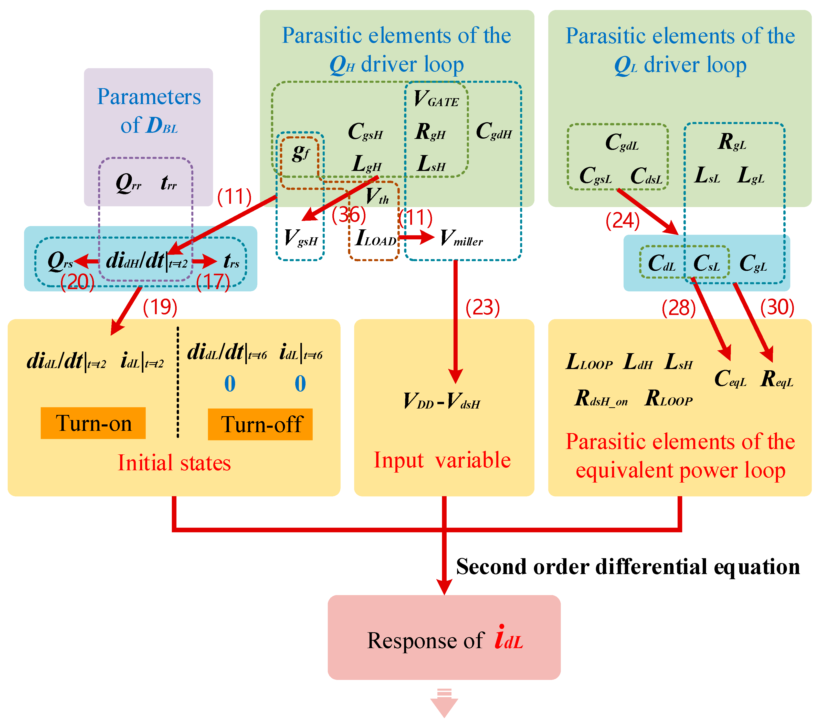
According to the analyses in Section 2, the crosstalk phenomenon lasts almost throughout the whole switching process of the bridge-arm and different parasitic elements are coupled in different switching stages. It is necessary to consider the parasitic elements specifically and their correlative effects on the related variables in each stage should be studied deeply. Establishing accurate models of them is an important step for the crosstalk analysis. So, the modeling of special parameters and main variables are provided first, based on them, a crosstalk model can be derived in detail.
3.1. Model Establishments of Special Parameters and Main Variables
3.1.1. Nonlinear Capacitances
The device manufacturer provides the curves of the input capacitance Ciss, the output capacitance Coss, and the reverse capacitance Crss in the datasheet in general. According to the method provided in Refs. [26,27], the values of them can be piecewise fitted with high precision, which can be described by the equation
where Cj0 is the capacitance value when Vds = 0, Vj is the built-in voltage and can be treated as an undetermined coefficient, m is the capacitance gradient factor. They can be adjusted according to the range of Vds. Figure 8 shows the fitted capacitances simulation curves compared with the datasheet curves.
Interelectrode capacitances are usually used in actual model establishment and calculations, which can be extracted according to Equation (10). Their comparison with the datasheet curves is shown in Figure 9. Since Cgs and Cds are much larger than Cgd, the interelectrode capacitances curves are almost the same with the parasitic capacitance curves from the datasheet.
3.1.2. Current Switching Rate and Reverse Recovery Current of DBL
Essentially, the current switching rate is determined by the active-controlled device. When QH works in the saturation region, QH is modeled as a dependent current source controlled by VgsH. The expression of the channel current is given by
where ich is the channel current of QH, gf is the transconductance coefficient and it remains at the maximum. The rising rate of VgsH is entirely dependent on the driver loop characteristics of QH. It worth noting that the induced voltage on LsH is superimposed in the driver loop, which provides negative feedback to the driver loop [21,37]. This factor restricts the rising rate of VgsH and makes the current switching rate reach a maximum. The circuit equations of the QH driver loop can be expressed as
where VidsH is induced voltage on LsH caused by the changing of idH
When the current switching rate reaches the maximum, the induced voltage of the parasitic inductances of the power loop remains constant, and the interelectrode capacitances do not have charge current, thus, the current of the power loop can be considered as idH = ich.
In Stage 2, when the channel current rises to ILOAD, the freewheeling current of DBL drops to zero and starts the reverse recovery process, idL increases in a positive direction and its rate remains the same as the drop rate before, it is because the equilibrium state remains unchanged (the characteristics of the QH driver loop and the transconductance). In order to obtain the rising duration of the reverse recovery current, the diode model in reference [38] is employed, which separates the reverse recovery process and charging process of junction capacitance into two stages. It is more suitable to describe the processes of current rising and voltage build-up respectively, as is shown in Figure 10. In general, the reverse recovery charge given in the datasheet is the charge for the entire reverse recovery process, Qrr; thus, the charge of the reverse recovery process, Qrs, needs to derive according to the provided test conditions. The equations are established as follows:
The test conditions are listed in Table 1, the relationship between Qrs and Qrr can be derived as Equation (20).
Therefore, in the analysis of the actual current switching of the bridge-arm, according to Qrs and the rising rate of idL, the reverse recovery current value at the time of DBL turning to the reverse-biased can be obtained, which is the initial condition of the voltage switching response in the next stage.
3.1.3. Voltage Switching Rate
The impact of the voltage switching is the most obvious source factor on the crosstalk. In the bridge-arm configuration, the voltage switching is controlled by the active-controlled device. When the drain-source voltage of the active-controlled device changes, the drain-source voltage of the passive device changes accordingly to keep the bus supply voltage constant.
For the active-controlled SiC MOSFET, QH, the current discharges Cgd in this stage, meanwhile, Vgs is clamped to the Vmiller and keeps constant, which has been well known as miller platform voltage. the gate driver works like a current source. There is not a significant charging current through CgsH. ig can be express as
VgsH keeps at Vmiller, which has a clamping effect on the driver loop, the maximum current that the driver loop can reach is limited. Therefore, igH remains constant, and the induced voltage on the parasitic inductances of the driver loop can be ignored. The driver loop equation of QH can be expressed as
where VidsH is induced voltage on LsH caused by idH. Combining (14), (21), and (22), the switching rate of VdsH can be obtained as
It can be seen from (23) that the nonlinear variation of VdsH is affected by the nonlinear characteristics of CgdH and the rate of idH. In addition, the common source parasitic inductance LsH provides negative feedback to the switching rate of VdsH. In the turn-on process, since the reverse recovery current decrease, a negative induced voltage is generated on LsH, which will increase the drop rate of VdsH. Conversely, it suppresses the rising rate of VdsH in the turn-off process.
Due to the parasitic inductances exist in the power loop, the response of VdsL cannot be directly described as a reversed response of VdsH. In this paper, VdsL is equivalent to a response of the whole parasitic capacitances of QL charged by the applied voltage VDD − VdsH, where all the parasitic inductances of the power loop and the driver loop branch are taken into consideration. The equivalent circuits are shown in Figure 11. In this way, an accurate nonlinear input is given from the source and the influences of parasitic elements are thoroughly considered. These settings can ensure the accuracy of the response of VdsL.
Furthermore, for the turn-on voltage switching stage (Stage 3), the rising of VdsL is accompanied by the reverse recovery process of DBL (the blocking voltage building up), there are the initial value and rate of the drain current, idL|t = t2 and didL/dt|t = t2, at the end time of Stage 2, which can be obtained from Section 2. For the whole structs of QL, the reverse recovery model of the independently packaged freewheeling diode applied in Refs. [21,38] is inadequate to describe the drain-source voltage building process. It is because the freewheeling diode is inversely paralleled with the SiC MOSFET; hence, all the parasitic capacitances need to be considered. The independent barrier capacitance charge model will bring about dynamic accumulation errors for the response of VdsL. To sum up, combining with the bridge-arm structure, all the factors of the reverse recovery current and the parasitic elements should be considered as a whole in this stage.
The capacitances, CgsL, CgdL, and CdsL are in delta connection and the driver loop is paralleled with CgsL and LsL. The delta connection of capacitances can be transformed into the star connection, CgL, CdL, and CsL [39], as shown in Figure 12a. The expressions of capacitances, CgL, CdL, and CsL are given as follows
Considered from the perspective of the power loop, the paralleled driver loop and the CsL-LsL branch can be further regarded as the equivalent impedance to evaluate its impact. The impedance of the driver loop can be expressed as
The impedance of the CsL-LsL branch is expressed as
where ωn_P is the resonance frequency of the power loop and it can be approximated by
The total equivalent impedance of the lower SiC MOSFET the power loop is
The equivalent damping resistance is determined by the ratio of current flowing through RgL and the total current of the power loop, which can be expressed by Equation (30).
Thus, the power loop is equivalent to a second-order circuit, as shown in Figure 12b. The total equivalent resistance can be express by
The power loop equations can be modeled as
It is worth noting that the nonlinear changes of Cg, Cd, and Cs also need to consider. They can be derived according to the curves of interelectrode capacitances, which is shown in Figure 13.
When VdsH drops to the on-state voltage VdsH_on (Stage 4), although QH enters the ohmic region, VdsL of QL will continue to oscillate after it rises to VDD due to the RLC characteristic of the power loop. The ideal voltage division given in [24] cannot be used here, since it does not take into account the power loop oscillation. In Stage 4, the supply voltage is VDD-VdsH_on and the equivalent circuit is shown in Figure 14. The structure of the equivalent circuit is the same as in the previous stage and the expressions of CeqL and ReqL can also be described as (28) and (30). The power loop equation is transformed from (32) to (34).
In the turn-off process, the circuit topologies transformations for the analysis of the voltage and current switching stages are the same as those in the turn-on stages. The voltage and current switching rates are still controlled by QH. The only difference is that the initial value and rate of the drain current are zero at the beginning of Stage 6.
3.2. Analytical Model of Crosstalk
During the current switching stages (Stage 2 and Stage 7), VdsL does not change, only the induced voltage on the common source parasitic inductance, LsL, affects the driver loop, combining the equations of the driver loop (2), (3) with the equations of the channel currents (11)–(14), the response of VgsL is correlated with VgsH ultimately:
During the voltage switching stages (Stage 3 and Stage 6), it can be generalized that the initial state of the drain current, the nonlinear switching rate of the drain-source voltage, the parasitic inductances of the power loop and common source, and the nonlinear characteristics of the interelectrode capacitances affect the response of VdsL. Through the analysis in section A. All these factors can be further directly or indirectly linked with the response of idL. idL becomes a key vinculum to reflect the impacts of the voltage switching. The correlations are summarized in Figure 15.
Combining (31)–(33) with (23), idL can be expressed as
After VdsL rises to VDD in the turn-on process, idL is expressed as
Next, idL is used as an input source to analyze its influence on the crosstalk of the driver loop. The interelectrode capacitances can be converted into two branches with the delta-star transformation, which helps simplify the analysis. The current flowing through CdL is idL. From the perspective of the driver loop, the crosstalk response is converted to the voltage difference between CsL and CgL on the two branches. The equivalent circuit is shown in Figure 16 and the equations can be established as
Therefore, the relationship of igL and idL can be obtained as follow
VgsL can be expressed by
where CeqL_d = CgLCsL/(CgL + CsL). Finally, the response of VgsL can be deducted by correlating the differential Equations (37), (44), and (45).
So far, the crosstalk responses of the turn-on and turn-off processes are fully expressed in the time domain. The Equations (35), (44), and (45) can be discretized and brought into MATLAB, where the directly correlated variable responses are expressed by Equations (36)–(38). Based on the software, the whole simulation waveforms of VgsL can be presented minutely and accurately. The detailed simulation and experimental verification are described in the next section.
4. Simulation and Experimental Verification
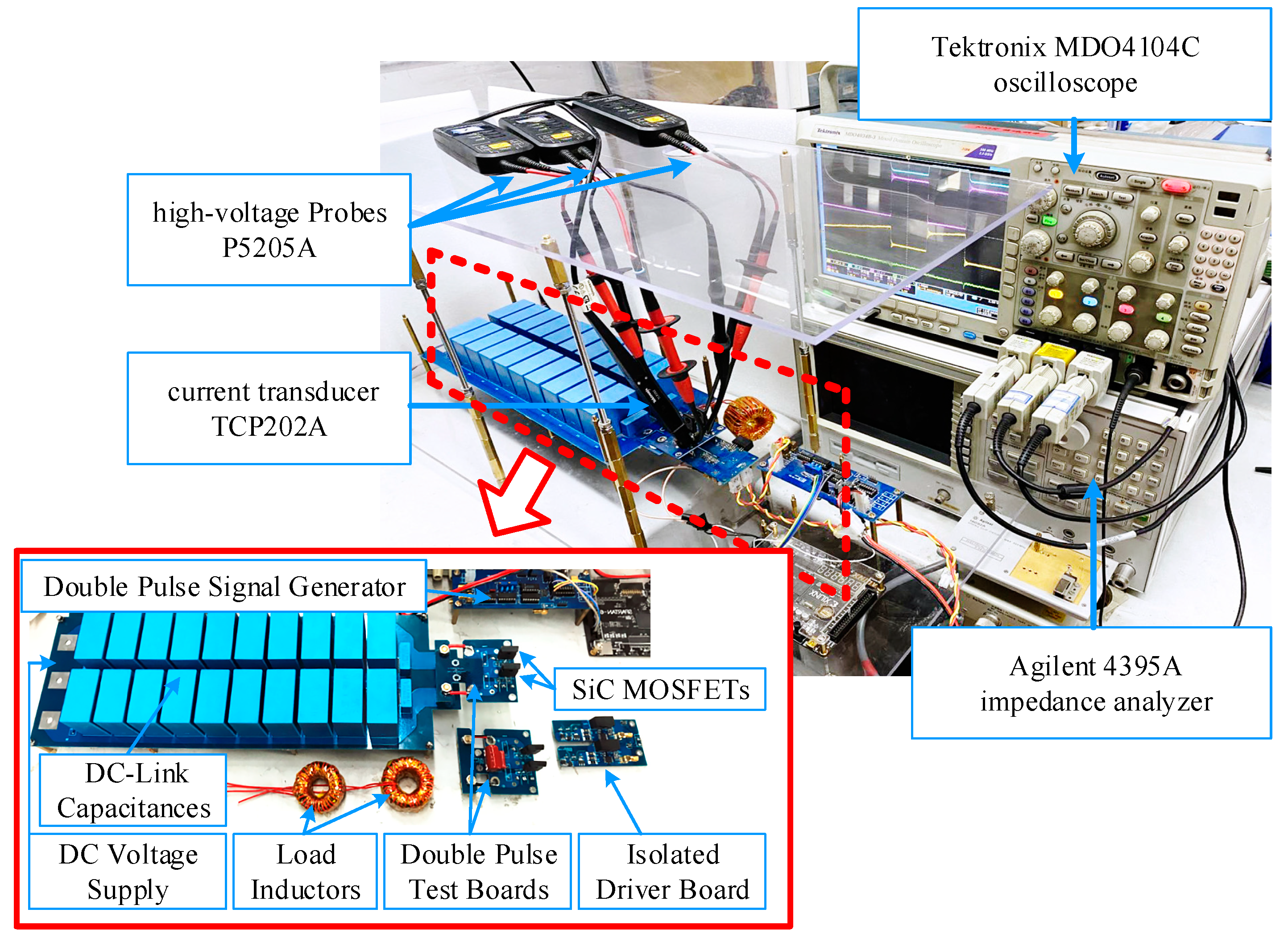
To verify the analysis and modeling method in the previous section, a typical double pulse test circuit platform is built, Figure 17 shows the photograph of the test platform. Two 1200 V/36 A SiC MOSFETs C2M0080120D, from Wolfspeed corporation, are connected in series as the upper and lower switching devices of the bridge-arm, a 12 μH ferrite-core inductance is connected in parallel with the lower SiC MOSFET as the load inductance. The test circuit is supported by 600 V DC supply voltage, multiple groups of 10 μF capacitances are connected in parallel with the DC input terminal to ensure the voltage stability. The initial parameters of the circuit model are listed in Table 2. Some fixed parameter values were obtained through the datasheet, including Qrr, gf, Rg_in, and Rds_on. The values of parasitic inductances were implemented by an ANSYS Q3D Extractor finite-element analysis (FEA) simulation, which includes internal pins of the devices and the printed circuit board (PCB) layout [40], The external pins of the devices and the connecting leads of the power loop were measured by an Agilent 4395A impedance analyzer.
The circuit setting and the parameter values in the simulation calculations are based on this real circuit experiment platform within a reasonable range. The nonlinear capacitances are piecewise fitted according to the datasheet, the piecewise parameters are listed in Table 3. This piecewise fitting model can be invoked as independent computing units based on the values of VdsH and VdsL to obtain the precise value in every discrete computing period.
In order to distinguish the response stages and accurately divide the related factors of crosstalk in different stages, the terminal value of the current response in Stage 2 and Stage 7 and the voltage response in Stage 3 and Stage 6 need to be identified as the switching judgment conditions. They are listed in Table 4 and the equations also need to be added to the simulation calculation program.
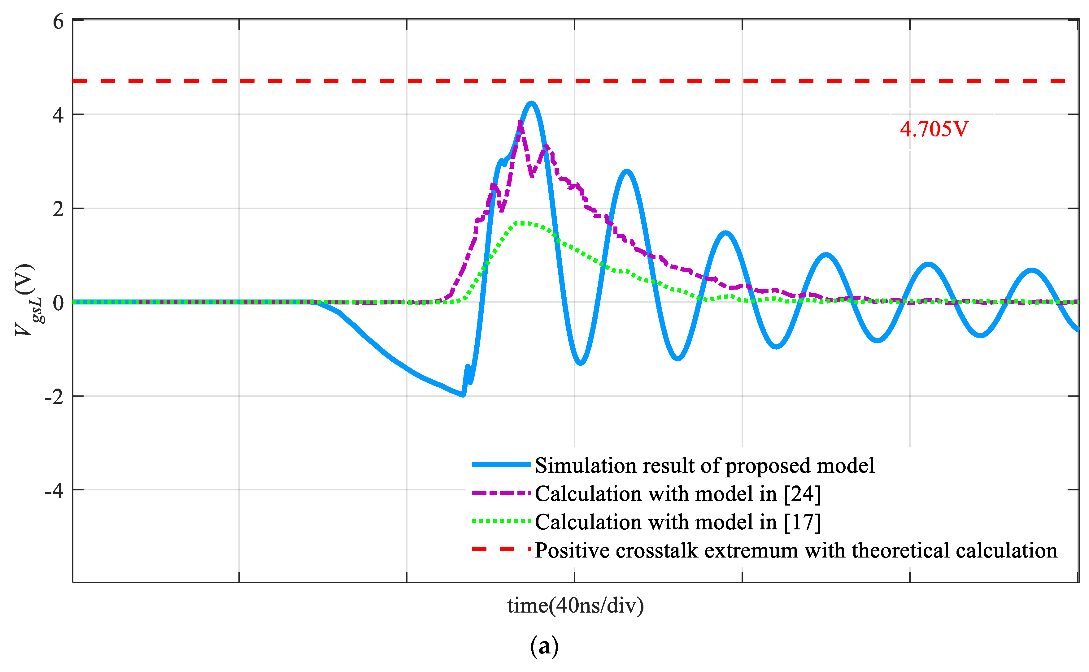
According to the piecewise conditions, the crosstalk response can be calculated stage-by-stage with iterative method, by discretizing the equations, it is convenient to obtain the numerical solution of the variable responses. The simulated waveforms of crosstalk, when VDD = 600 V and ILOAD = 20 A, are shown in Figure 18. In addition, the calculation results according to the model presented in the literature [17,24], and the theoretical extremum of crosstalk [15] are also placed on the same coordinates to horizontal compare the differences.
It can be seen from Figure 18, during the current switching stages in the turn-on process, there is a drop on VgsL, which reflects the impacts of the common source parasitic inductance with the rapid current changes. However, the calculations in Refs. [17,24] do not consider the influence of the parasitic inductances, so that there is a significant difference in the negative fluctuations of the crosstalk. There are trends in our data to suggest that the positive peak value of crosstalk is higher compared with the calculation in Ref. [24]. VgsL will continue to rise and start oscillating after the voltage switching process, which embodies the coupling effect of the oscillation caused by the parasitic inductance and parasitic capacitance of the power loop on the crosstalk. In the turn-off process, the negative peak value of the crosstalk proposed in this paper is higher than the calculated value in Ref. [24], which is also due to the influence of parasitic inductance. More specifically, during the voltage switching stages (Stage 6), the parasitic capacitances of QL are discharged with the decrease of VdsL, the displacement current of CgdL induces a negative fluctuation in VgsL, but the discharge current for CdsL starts to increase from zero, which causes a negative induced voltage on LsL, thus, it will suppress the negative fluctuation of VgsL. Further, the simulation results of the crosstalk peak values given in this paper and Ref. [24] are both significantly larger than the calculation results with constant capacitances, these all indicate that the nonlinear parasitic capacitances have obvious influences on the crosstalk evaluation.
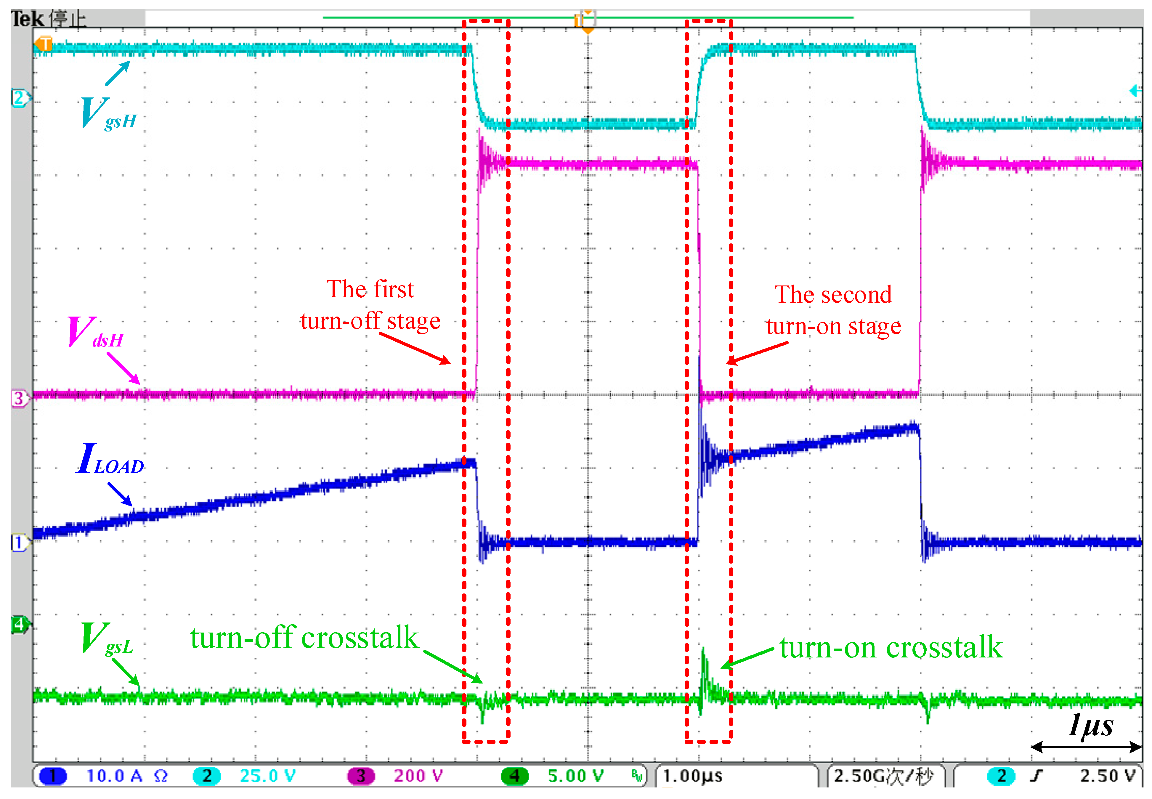
The experimental platform is employed to verify the correctness of the proposed model. In the experimental test, since there is no any crosstalk suppression method, to prevent spurious trigger, the negative driver voltage level of QL is set at −5 V. Adjusting the negative voltage bias does not have a significant effect on the responses of crosstalk voltage [24]. The double pulse trigger signal position is adjusted to set the load current at 20 A. The first turn-off and the second turn-on waveforms are extracted in this paper due to the drain current value almost maintain the same at the switching time, as is shown in Figure 19. Figure 20 compares the experiment results and the simulation results of crosstalk waveforms in the turn-on and turn-off process, the experimental data are uniformly added 5 V to facilitate the comparisons. The red lines represent the experiment waveforms and the blue lines represent the simulation waveforms.
It is apparent that the proposed analytical model is more detailed and matches better with the experimental results (in terms of the voltage drop in Stage 2, the oscillations after the voltage switching, and the peak values response) than models in Refs. [17,24]. There are deviations between the simulation and actual results of the oscillation frequencies, it is because the measurement deviation of parasitic inductances and equivalent resistance of the circuit, and the model of the nonlinear capacitances is difficult to maintain a high consistency with the data in the datasheet. These deviations are inevitable but the variation trends can still be correctly inferred.
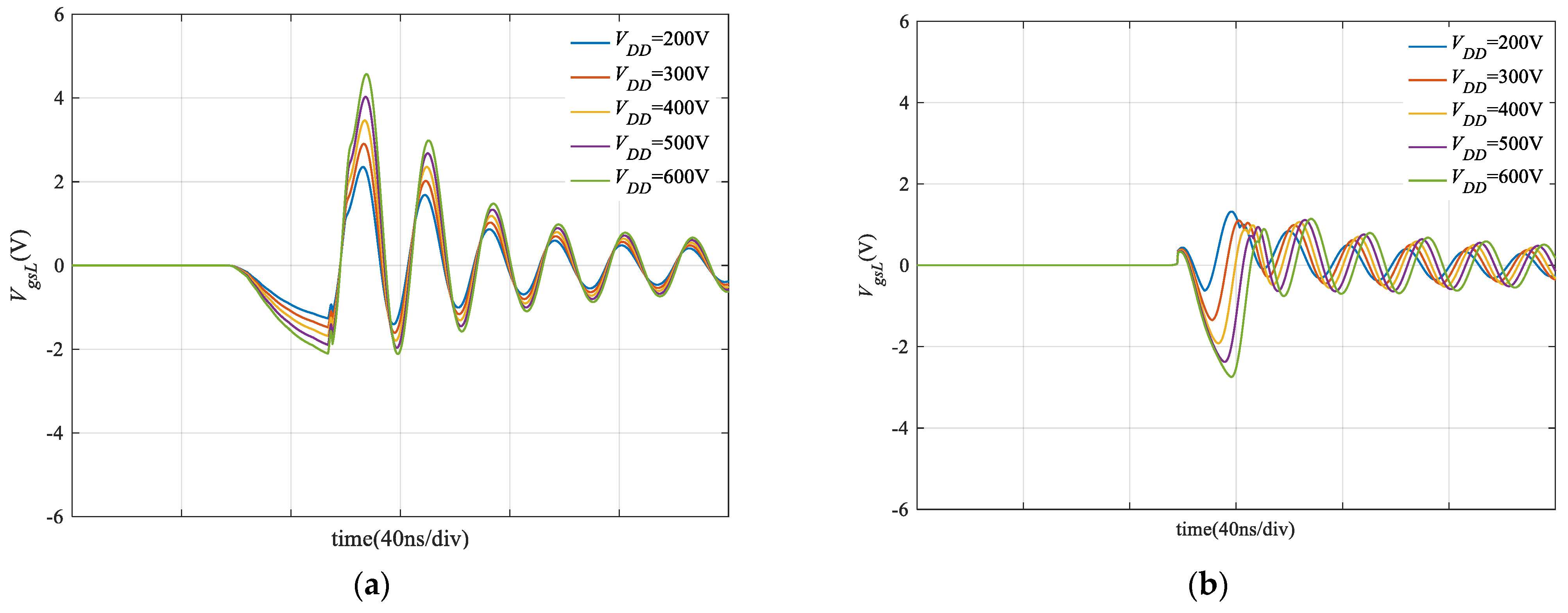
According to the previous analysis, the variables that directly impact the crosstalk are the current and voltage switching rates and they are closely related to the driver capability of the active-controlled device. In the simulations and experiments, adjusting the driver resistant RgH to change the switching rate of the bridge-arm, this method can adjust both voltage and current switching rates according to (11)–(14) and (23). The simulations and experiments waveforms of crosstalk are shown in Figure 21, and the trend comparisons of the relative crosstalk peak values are provided in Figure 22.
It can be seen from Figure 21 and Figure 22 that the experimental waveforms and the variation trends of crosstalk are in good agreement with the simulation results, which verifies the correctness and the accuracy of the proposed model with the situations where the switching rates are dynamically adjusted. However, the deviations of the peak values between the simulation and experiment results also need to be noticed. Especially in the turn-on process, the measured amplitudes of VgsL are smaller than the calculated values. One of the main reasons is that the voltage measurement probes can only be connected between the external terminal nodes of the gate and source, thus the internal voltages of parasitic elements are included in the measurement values. During the turn-on process, the voltages on the internal gate resistance, the gate parasitic inductances, and the internal source parasitic inductances are all opposite to the gate-source voltage of CgsL, which leads to the measured peak values of VgsL are smaller than the calculated values. In addition, the reverse recovery current decreases rapidly from the beginning of the voltage switching stage, which produces a relatively larger negative induced voltage on the internal common source parasitic inductance. These two factors cause more obvious deviations of the crosstalk voltage in the turn-on process.
These measurement deviations are inevitable but the variation trend can still be correctly inferred, and importantly, the directly calculated analytical values of internal VgsL are essentially needed to evaluate the real crosstalk voltage response rather than the voltage between the external nodes. The measurement values can be considered as indirect reflections of the crosstalk. The precise values and errors of experimental measurements and simulation calculations for the relative amplitudes of the crosstalk are listed in Table 5.
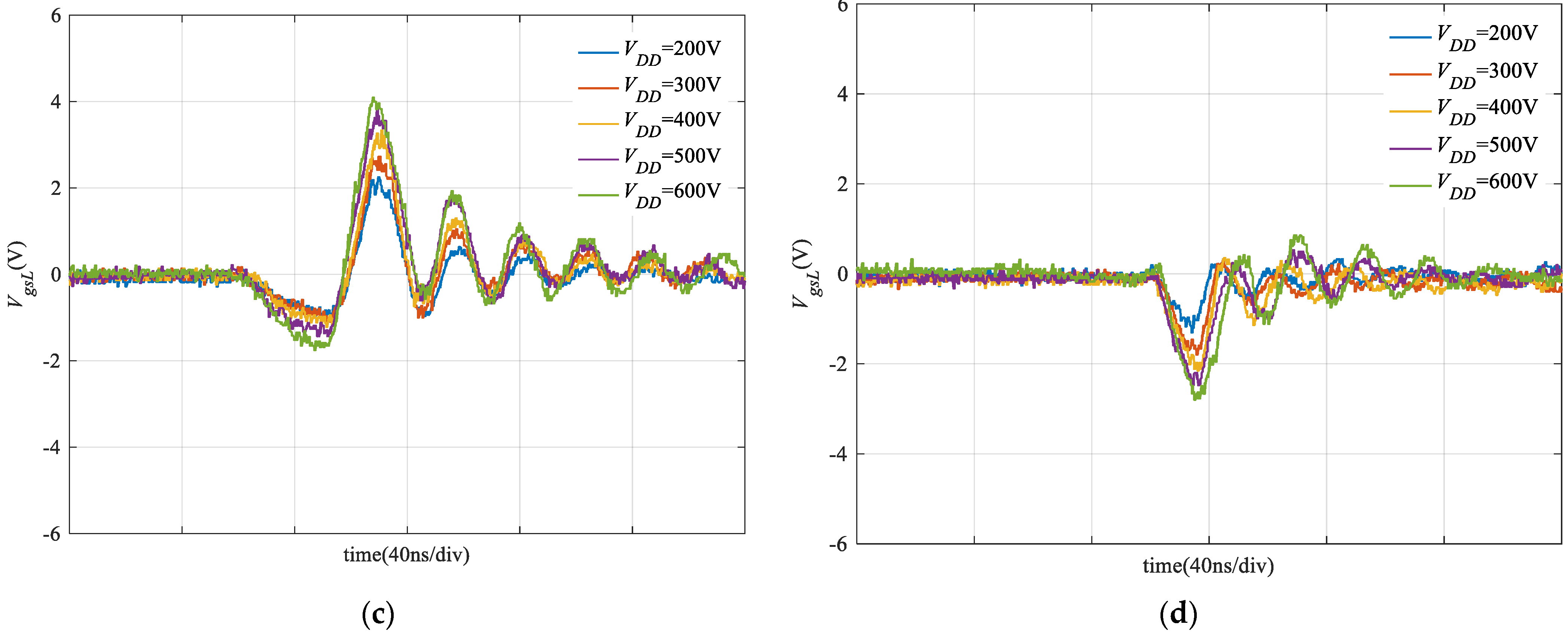
According to (32) and the judgment conditions of t3 and t6, the switching rate and duration of the voltage also changed with the different input voltage levels, which indirectly affects the crosstalk responses in the voltage switching process, especially the peak value. To verify the model in a further step, different DC voltages are applied to the double pulse test platform, while other test conditions are the same as the initial setting, the load current is kept at 20 A by adjusting the trigger position of the driver signal. VDD is increased from 200 V to 600 V with 100 V step. The simulation and experimental crosstalk waveforms with different VDD are shown in Figure 23. The precise values and errors of experimental measurements and simulation calculations for the relative amplitudes of the crosstalk are listed in Table 6.
As shown in Figure 23, the experimental waveforms of crosstalk agree well with the simulation results with the different supply voltage. Figure 24 shows the comparisons of the relative crosstalk peak values extracted from the experiments with the simulation results and the calculated values according to the algorithm of [24]. It can be seen that the crosstalk peaks simulated by the proposed model are more accurate than the crosstalk peaks values calculated based on the method in [24]. This can be attributed to the errors caused by the parasitic inductances, especially in the turn-off process, the induced voltage on LsL and the impedance of the driver loop have opposite effects on the fluctuation of VgsL, which causes greater deviations.
5. Conclusions
In this paper, a detailed and accurate analytical model of crosstalk for SiC MOSFETs bridge-leg configuration is proposed. The source impact variables and the critical parasitic elements to the crosstalk are comprehensively considered. The critical factors of SiC MOSFETs and bridge-arm are taken into account, including the nonlinear characteristics of the interelectrode capacitances, the reverse recovery characteristics of the anti-parallel diodes, the parasitic inductances of the power loop, and the nonlinear voltage switching and damping oscillation process. Their direct or indirect coupling effects to the crosstalk in different switching stages are analyzed. Combining with these factors, the proposed model covers the whole crosstalk response of the bridge-arm switching processes and the equivalent analysis circuits of each switching stage are established. The correctness and the accuracy of the proposed model are validated by simulation and experiment. Compared with the current crosstalk model, the proposed model can present more details and accurately of crosstalk prediction and is closer to the practical engineering application. The proposed model can be employed to evaluate the crosstalk responses to ensure the stability and reliability of bridge-arms, and can also be used in the design and development of power converters to reduce loss and play full operation performances of SiC MOSFETs. In future work, the influence trends of the parasitic elements and variables on the crosstalk response can be detailed analyzed based on the model. It should be noticed that the temperature characteristics of the model are not concerned in this paper, this may cause deviations between the modeling values and the actual values of parasitic parameters, and in practical projects, the temperature of the switching devices of power converters varies with the operating time. Thus, the improved analytical model for crosstalk with considering temperature characteristics will be studied in future work to improve the accuracy.
Author Contributions
Conceptualization, D.Y. and X.W.; methodology, D.Y.; validation, D.Y. and X.W.; formal analysis, D.Y.; investigation, D.Y. and X.W.; writing—original draft preparation, D.Y.; review and editing, Y.Z. and X.W.; supervision, Y.Z.; project administration, Y.Z. All authors have read and agreed to the published version of the manuscript.
Funding
This work was supported by the Strategic Priority Research Program of the Chinese Academy of Sciences XDA14020400.
Conflicts of Interest
The authors declare no conflict of interest.
References
- Liang, Z.; Ning, P.; Wang, F. Development of Advanced All-SiC Power Modules. IEEE Trans. Power Electron. 2014, 29, 2289–2295. [Google Scholar] [CrossRef]
- Garrido-Diez, D.; Baraia, I. Review of wide bandgap materials and their impact in new power devices. In Proceedings of the 2017 IEEE International Workshop of Electronics, Control, Measurement, Signals and their Application to Mechatronics (ECMSM), Donostia-San Sebastian, Spain, 24–26 May 2017; pp. 1–6. [Google Scholar]
- Zhao, Z.; He, X. Research on Digital Synchronous Rectification for a High-Efficiency DC-DC Converter in an Auxiliary Power Supply System of Magnetic Levitation. Energies 2019, 13, 51. [Google Scholar] [CrossRef] [Green Version]
- Biela, J.; Schweizer, M.; Waffler, S.; Kolar, J.W. SiC versus Si—Evaluation of Potentials for Performance Improvement of Inverter and DC–DC Converter Systems by SiC Power Semiconductors. IEEE Trans. Ind. Electron. 2011, 58, 2872–2882. [Google Scholar] [CrossRef]
- Wang, Z.; Shi, X.; Xue, Y.; Tolbert, L.M.; Wang, F.; Blalock, B.J. Design and Performance Evaluation of Overcurrent Protection Schemes for Silicon Carbide (SiC) Power MOSFETs. IEEE Trans. Ind. Electron. 2014, 61, 5570–5581. [Google Scholar] [CrossRef]
- Funaki, T. A study on self turn-on phenomenon in fast switching operation of high voltage power MOSFET. In Proceedings of the 2013 3rd IEEE CPMT Symposium Japan, Kyoto, Japan, 11–13 November 2013; pp. 1–4. [Google Scholar]
- Zaman, H.; Wu, X.; Zheng, X.; Khan, S.; Ali, H. Suppression of Switching Crosstalk and Voltage Oscillations in a SiC MOSFET Based Half-Bridge Converter. Energies 2018, 11, 3111. [Google Scholar] [CrossRef] [Green Version]
- Zhang, Z.; Zhang, W.; Wang, F.; Tolbert, L.M.; Blalock, B.J. Analysis of the switching speed limitation of wide band-gap devices in a phase-leg configuration. In Proceedings of the 2012 IEEE Energy Conversion Congress and Exposition (ECCE), Raleigh, NC, USA, 15–20 September 2012; pp. 3950–3955. [Google Scholar]
- Chen, Z.; Boroyevich, D.; Burgos, R.; Wang, F. Characterization and modeling of 1.2 kv, 20 A SiC MOSFETs. In Proceedings of the 2009 IEEE Energy Conversion Congress and Exposition, San Jose, CA, USA, 20–24 September 2009; pp. 1480–1487. [Google Scholar]
- Merienne, F.; Roudet, J.; Schanen, J. Switching disturbance due to source inductance for a power MOSFET: Analysis and solutions. In Proceedings of the PESC Record. 27th Annual IEEE Power Electronics Specialists Conference, Baveno, Italy, 23–27 June 2002; Volume 2, pp. 1743–1747. [Google Scholar]
- Wang, Q. The Impact of Parasitic Elements on Spurious Turn-On in Phase-Shifted Full-Bridge Converters. J. Power Electron. 2016, 16, 883–893. [Google Scholar] [CrossRef] [Green Version]
- Jahdi, S.; Alatise, O.; Alexakis, P.; Ran, L.; Mawby, P. The Impact of Temperature and Switching Rate on the Dynamic Characteristics of Silicon Carbide Schottky Barrier Diodes and MOSFETs. IEEE Trans. Ind. Electron. 2015, 62, 163–171. [Google Scholar] [CrossRef] [Green Version]
- Yin, S.; Tseng, K.J.; Tong, C.F.; Simanjorang, R.; Gajanayake, C.J.; Nawawi, A.; Liu, Y.; Liu, Y.; See, K.Y.; Sakanova, A.; et al. Gate driver optimization to mitigate shoot-through in high-speed switching SiC half bridge module. In Proceedings of the 2015 IEEE 11th International Conference on Power Electronics and Drive Systems, Sydney, NSW, Australia, 9–12 June 2015; pp. 484–491. [Google Scholar]
- Wang, P.; Zhang, L.; Lu, X.; Sun, H.; Wang, W.; Xu, D. An Improved Active Crosstalk Suppression Method for High-Speed SiC MOSFETs. IEEE Trans. Ind. Appl. 2019, 55, 7736–7744. [Google Scholar] [CrossRef]
- Elbanhawy, A. Limiting Cross-Conduction Current in Synchronous Buck Converter Designs; Note AN-7019; Fairchild Semiconductor: San Jose, CA, USA, 2005. [Google Scholar]
- Zhou, Q.; Gao, F. A gate driver of SiC MOSFET for suppressing the negative voltage spikes in a bridge circuit. In Proceedings of the 2016 IEEE Applied Power Electronics Conference and Exposition (APEC), Long Beach, CA, USA, 20–24 March 2016; pp. 536–543. [Google Scholar]
- Wu, T. Cdv/dt induced turn-on in synchronous buck regulators. Proc. Appl. Manual-Int. Rectifier 2012, 1–6. [Google Scholar]
- Li, Y.; Liang, M.; Chen, J.; Zheng, T.Q.; Guo, H. A Low Gate Turn-OFF Impedance Driver for Suppressing Crosstalk of SiC MOSFET Based on Different Discrete Packages. IEEE J. Emerg. Sel. Top. Power Electron. 2019, 7, 353–365. [Google Scholar] [CrossRef]
- Nishigaki, A.; Umegami, H.; Hattori, F.; Martinez, W.; Yamamoto, M. An analysis of false turn-on mechanism on power devices. In Proceedings of the 2014 IEEE Energy Conversion Congress and Exposition (ECCE), Pittsburgh, PA, USA, 14–18 September 2014; pp. 2988–2993. [Google Scholar]
- Jahdi, S.; Alatise, O.; Gonzalez, J.A.O.; Bonyadi, R.; Ran, L.; Mawby, P. Temperature and Switching Rate Dependence of Crosstalk in Si-IGBT and SiC Power Modules. IEEE Trans. Ind. Electron. 2016, 63, 849–863. [Google Scholar] [CrossRef] [Green Version]
- Wang, J.; Chung, H.S.-H. Impact of Parasitic Elements on the Spurious Triggering Pulse in Synchronous Buck Converter. IEEE Trans. Power Electron. 2014, 29, 6672–6685. [Google Scholar] [CrossRef]
- Elferich, R.; López, T. Impact of Gate Voltage Bias on Reverse Recovery Losses of Power MOSFETs. In Proceedings of the Twenty-First Annual IEEE Applied Power Electronics Conference and Exposition, APEC ’06, Dallas, TX, USA, 19–23 March 2006; p. 6. [Google Scholar]
- Zhang, B.; Xie, S.; Xu, J.; Qian, Q.; Zhang, Z.; Xu, K. A Magnetic Coupling Based Gate Driver for Crosstalk Suppression of SiC MOSFETs. IEEE Trans. Ind. Electron. 2017, 64, 9052–9063. [Google Scholar] [CrossRef]
- Li, H.; Jiang, Y.; Qiu, Z.; Wang, Y.; Ding, Y. A Predictive Algorithm for Crosstalk Peaks of SiC MOSFET by Considering the Nonlinearity of Gate-Drain Capacitance. IEEE Trans. Power Electron. 2021, 36, 2823–2834. [Google Scholar] [CrossRef]
- Mudholkar, M.; Ahmed, S.; Ericson, M.N.; Frank, S.S.; Britton, C.L.; Mantooth, H.A. Datasheet Driven Silicon Carbide Power MOSFET Model. IEEE Trans. Power Electron. 2013, 29, 2220–2228. [Google Scholar] [CrossRef]
- Costinett, D.; Maksimovic, D.; Zane, R. Circuit-Oriented Treatment of Nonlinear Capacitances in Switched-Mode Power Supplies. IEEE Trans. Power Electron. 2015, 30, 985–995. [Google Scholar] [CrossRef]
- Chen, K.; Zhao, Z.; Yuan, L.; Lu, T.; He, F. The Impact of Nonlinear Junction Capacitance on Switching Transient and Its Modeling for SiC MOSFET. IEEE Trans. Electron Devices 2015, 62, 333–338. [Google Scholar] [CrossRef]
- Duan, Z.; Fan, T.; Wen, X.; Zhang, D. Improved SiC Power MOSFET Model Considering Nonlinear Junction Capacitances. IEEE Trans. Power Electron. 2018, 33, 2509–2517. [Google Scholar] [CrossRef]
- Ho, C.N.M.; Canales, F.; Coccia, A.; Laitinen, M. A Circuit-Level Analytical Study on Switching Behaviors of SiC Diode at Basic Cell for Power Converters. In Proceedings of the 2008 IEEE Industry Applications Society Annual Meeting, Edmonton, AB, Canada, 5–9 October 2008; pp. 1–8. [Google Scholar]
- Chen, Z.; Amaro, I. Optimizing low side gate resistance for damping phase node ringing of synchronous buck converter. In Proceedings of the 2012 IEEE Energy Conversion Congress and Exposition (ECCE), Raleigh, NC, USA, 15–20 September 2012; pp. 1827–1832. [Google Scholar]
- Xue, P.; Maresca, L.; Riccio, M.; Breglio, G.; Irace, A. Analysis on the Self-Sustained Oscillation of SiC MOSFET Body Diode. IEEE Trans. Electron Devices 2019, 66, 4287–4295. [Google Scholar] [CrossRef]
- Bi, C.; Lu, R.; Li, H. Prediction of Electromagnetic Interference Noise in SiC MOSFET Module. IEEE Trans. Circuits Syst. II Express Briefs 2019, 66, 853–857. [Google Scholar] [CrossRef]
- Yang, J.; Feng, G.; Huadong, L.; Suhong, C. Characterization and Detailed Analysis of the Crosstalk with SiC MOSFET. In Proceedings of the 2018 1st Workshop on Wide Bandgap Power Devices and Applications in Asia (WiPDA Asia), Xi’an, China, 16–18 May 2018; pp. 239–243. [Google Scholar] [CrossRef]
- Wang, J.; Chung, H.S.-H.; Li, R.T.-H. Characterization and Experimental Assessment of the Effects of Parasitic Elements on the MOSFET Switching Performance. IEEE Trans. Power Electron. 2013, 28, 573–590. [Google Scholar] [CrossRef]
- Liang, M.; Zheng, T.Q.; Li, Y. An Improved Analytical Model for Predicting the Switching Performance of SiC MOSFETs. J. Power Electron. 2016, 16, 374–387. [Google Scholar] [CrossRef] [Green Version]
- Christen, D.; Biela, J. Analytical Switching Loss Modeling Based on Datasheet Parameters for mosfets in a Half-Bridge. IEEE Trans. Power Electron. 2019, 34, 3700–3710. [Google Scholar] [CrossRef]
- Li, X.; Jiang, J.; Huang, A.Q.; Guo, S.; Deng, X.; Zhang, B.; She, X. A SiC Power MOSFET Loss Model Suitable for High-Frequency Applications. IEEE Trans. Ind. Electron. 2017, 64, 8268–8276. [Google Scholar] [CrossRef]
- Lauritzen, P.; Ma, C. A simple diode model with reverse recovery. IEEE Trans. Power Electron. 1991, 6, 188–191. [Google Scholar] [CrossRef]
- Clarks, K.A.; Matthew, N.O.S. Fundamentals of Electric Circuits, 5th ed.; McGraw-Hill: New York, NY, USA, 2013; pp. 52–58. [Google Scholar]
- Liu, Z.; Huang, X.; Lee, F.C.; Li, Q. Package Parasitic Inductance Extraction and Simulation Model Development for the High-Voltage Cascode GaN HEMT. IEEE Trans. Power Electron. 2014, 29, 1977–1985. [Google Scholar] [CrossRef]
Figure 1.
Equivalent model of double pulse test circuit and the parasitic elements of SiC MOSFET and bridge arm.
Figure 1.
Equivalent model of double pulse test circuit and the parasitic elements of SiC MOSFET and bridge arm.

Figure 2.
Structures of discrete SiC MOSFET with non-Kelvin package and Kelvin package. (a) non-Kelvin package (TO-247-3). (b) Kelvin package (TO-247-4).
Figure 2.
Structures of discrete SiC MOSFET with non-Kelvin package and Kelvin package. (a) non-Kelvin package (TO-247-3). (b) Kelvin package (TO-247-4).

Figure 3.
Qualitative analytical switching sequence of turn-on and turn-off stages.

Figure 4.
Equivalent circuit of QL for crosstalk analysis during turn-on process. (a) current decrease stage. (b) voltage rise stage.
Figure 4.
Equivalent circuit of QL for crosstalk analysis during turn-on process. (a) current decrease stage. (b) voltage rise stage.

Figure 5.
Equivalent circuit of QL for crosstalk analysis during turn-off process. (a) voltage drop stage. (b) current rise stage.
Figure 5.
Equivalent circuit of QL for crosstalk analysis during turn-off process. (a) voltage drop stage. (b) current rise stage.

Figure 6.
Parasitic capacitances in relationship with the drain-source voltage.

Figure 7.
The formation of crosstalk in voltage switching stage of turn-on process.

Figure 8.
Comparison between the data from datasheet and the simulation.

Figure 9.
Comparison between the capacitances from datasheet and the interelectrode capacitances.

Figure 10.
Modeling of the reverse recovery process of the antiparallel freewheeling diode.

Figure 11.
Equivalent circuits for VdsL analysis circuit.

Figure 12.
Simplified equivalent circuit for bridge-arm in Stage 3. (a) Star connection equivalent circuit; (b) Second-order equivalent circuit.
Figure 12.
Simplified equivalent circuit for bridge-arm in Stage 3. (a) Star connection equivalent circuit; (b) Second-order equivalent circuit.

Figure 13.
Comparison between the equivalent capacitances and the interelectrode capacitances.

Figure 14.
Simplified equivalent circuit for bridge-arm in Stage 4. (a) Star connection equivalent circuit; (b) Second-order equivalent circuit.
Figure 14.
Simplified equivalent circuit for bridge-arm in Stage 4. (a) Star connection equivalent circuit; (b) Second-order equivalent circuit.

Figure 15.
Relationships of idL with the parameters of the bridge-arm.

Figure 16.
Equivalent circuit for the driver loop of QL.

Figure 17.
Photograph of the double pulse test platform.

Figure 18.
Crosstalk waveforms provided by the proposed analytical model, the analytical model in [17] the analytical model in [24], and the extremum calculated by theoretical calculation. (a) turn-on process. (b) turn-off process.


Figure 19.
Double plus test waveforms.

Figure 20.
Comparison of simulation and experimental waveforms of crosstalk in (a) turn-on process, (b) turn-off process.
Figure 20.
Comparison of simulation and experimental waveforms of crosstalk in (a) turn-on process, (b) turn-off process.

Figure 21.
Comparison of simulation and experimental waveforms of crosstalk with different RgH. (a,b): simulation. (c,d): experiment. Left: turn-on. Right: turn-off.
Figure 21.
Comparison of simulation and experimental waveforms of crosstalk with different RgH. (a,b): simulation. (c,d): experiment. Left: turn-on. Right: turn-off.

Figure 22.
Comparison of simulation and experimental variation trend of relative crosstalk peak value with different RgH. (a) turn-on. (b) turn-off.
Figure 22.
Comparison of simulation and experimental variation trend of relative crosstalk peak value with different RgH. (a) turn-on. (b) turn-off.

Figure 23.
Comparison of simulation and experimental waveforms of crosstalk with different VDD. (a,b): simulation. (c,d): experiment. Left: turn-on. Right: turn-off.
Figure 23.
Comparison of simulation and experimental waveforms of crosstalk with different VDD. (a,b): simulation. (c,d): experiment. Left: turn-on. Right: turn-off.


Figure 24.
Comparison of simulation and experimental variation trend of relative crosstalk peak value with different VDD. (a) turn-on. (b) turn-off.
Figure 24.
Comparison of simulation and experimental variation trend of relative crosstalk peak value with different VDD. (a) turn-on. (b) turn-off.


Table 1.
Antiparallel Freewheeling Diode Characteristics and Reverse Recovery Test Parameters.
| Parameter | Value | Test Condition |
|---|---|---|
| VDD (V) | 3.3 | Vgs = −5 V, ILOAD = 20 A, VDD = 800 V did/dt = 2400 A/us |
| trr (ns) | 32 | |
| Qrr (nC) | 192 |
Table 2.
Fixed Parameters Setup.
| Component | Parameter | Value | Parameter | Value |
|---|---|---|---|---|
| Power circuit setting | VDD | 600 V | RLOOP | 230 mΩ |
| IDD | 20 A | LLOOP | 32 nH | |
| Fixed parameters of upper and lower SiC MOSFET (C2M0080120D) | Vth | 3.3 V | Qrr | 192 nC |
| VGATE | +20 V/−5 V | VGATE | −5 V | |
| gf | 8.1 S | VSD | 3.3 V | |
| RdsH_on | 40 mΩ | RdsH_on | 40 mΩ | |
| RgH_ex | 10 Ω | RgL_ex | 10 Ω | |
| RgH_in | 4.6 Ω | RgL_in | 4.6 Ω | |
| LgH_in | 1.1 nH | LgL_in | 1.7 nH | |
| LgH_ex | 3.0 nH | LgL_ex | 2.8 nH | |
| LsH_in | 1.3 nH | LsL_in | 1.3 nH | |
| LsH_ex | 3.7 nH | LsL_ex | 3.4 nH | |
| LdH_in | 1.2 nH | LdL_in | 1.1 nH | |
| LdH_ex | 3.3 nH | LdL_ex | 3.6 nH |
Table 3.
Parameters of Capacitance Piecewise Fitting Model.
| Parameter | Vds Range (V) | ||||||
|---|---|---|---|---|---|---|---|
| Capacitance | Cj0 (pF) | Fitting Parameter | 0–9 | 9–20 | 20–35 | 35–500 | 500–1200 |
| Ciss | 1700 | Vj | 20 | 1 × 10⁻⁴ | 1 × 10⁻⁶ | ||
| m | 0.8 | 0.028 | 0.0125 | ||||
| Coss | 1650 | Vj | 5 | 0.3 | 1 × 10⁻⁷ | ||
| m | 0.9 | 0.39 | 0.13 | ||||
| Crss | 400 | Vj | 350 | 300 | 0.4 | 5 × 10⁻⁴ | 3 × 10⁻⁴ |
| m | 45 | 43 | 0.73 | 0.29 | 0.29 | ||
Table 4.
Switching Time and Calculations of Judgement Conditions.
| Switching Time | t1 | t2 | t3 | t6 | t7 | t8 |
|---|---|---|---|---|---|---|
| Judgement condition | VgsH > Vth | idL > Irr_peak | VdsH < Vth | VgsH < Vmiller | VdsL <0 | idL < -iLOAD |
| Calculate equations | (11), (12), and (13) VidsH = 0 | (10), (11), (12), and (13) | (22) integrated computation from t2 | (11), (12), and (13) VidsH = 0 | (22) integrated computation from t6 | (10), (11), (12), and (13) |
| Initial states | -- | VgsH|t=t1 dVgsH/dt|t= t1 | VDD idL|t=t2 didL/dt|t= t2 | -- | -- | idL|t=t7 didL/dt|t= t7 |
Table 5.
Comparison of Experiments and Simulations with Variable RgH.
| RgH (Ω) | 10 Ω | 14 Ω | 18 Ω | 22 Ω | 26 Ω | |
|---|---|---|---|---|---|---|
| Turn-on | Relative VgsL with Simulation (V) | 4.282 | 3.838 | 3.356 | 2.898 | 2.481 |
| Relative VgsL with Experiment (V) | 4.05 | 3.58 | 3.10 | 2.59 | 2.12 | |
| Difference compared with experiment | 5.73% | 7.21% | 8.26% | 11.89% | 17.03% | |
| Turn-off | Relative VgsL with Simulation (V) | −2.742 | −2.616 | −2.443 | −2.159 | −1.881 |
| Relative VgsL with Experiment (V) | −2.59 | −2.52 | −2.38 | −2.20 | −2.02 | |
| Difference compared with experiment | 5.87% | 3.81% | 2.65% | 1.86% | 6.88% |
Table 6.
Comparison of Experiments and Simulations with Variable VDD.
| VDD (V) | 200 | 300 | 400 | 500 | 600 | |
|---|---|---|---|---|---|---|
| Turn-on | Relative VgsL with Simulation (V) | 1.860 | 2.656 | 3.326 | 3.870 | 4.282 |
| Relative VgsL with Experiment (V) | 1.81 | 2.58 | 3.22 | 3.72 | 4.05 | |
| Difference compared with experiment | 2.76% | 1.46% | 3.29% | 4.03% | 5.73% | |
| Turn-off | Relative VgsL with Simulation (V) | −0.911 | −1.554 | −2.166 | −2.510 | −2.742 |
| Relative VgsL with Experiment (V) | −1.00 | −1.61 | −2.11 | −2.42 | −2.59 | |
| Difference compared with experiment | 8.90% | 3.48% | 2.65% | 3.72% | 5.87% |
Publisher’s Note: MDPI stays neutral with regard to jurisdictional claims in published maps and institutional affiliations. |
© 2021 by the authors. Licensee MDPI, Basel, Switzerland. This article is an open access article distributed under the terms and conditions of the Creative Commons Attribution (CC BY) license (http://creativecommons.org/licenses/by/4.0/).
Share and Cite
MDPI and ACS Style
Yuan, D.; Zhang, Y.; Wang, X. An Improved Analytical Model for Crosstalk of SiC MOSFET in a Bridge-Arm Configuration. Energies 2021, 14, 683. https://0-doi-org.brum.beds.ac.uk/10.3390/en14030683
AMA Style
Yuan D, Zhang Y, Wang X. An Improved Analytical Model for Crosstalk of SiC MOSFET in a Bridge-Arm Configuration. Energies. 2021; 14(3):683. https://0-doi-org.brum.beds.ac.uk/10.3390/en14030683
Chicago/Turabian StyleYuan, Dakang, Yiming Zhang, and Xuhong Wang. 2021. "An Improved Analytical Model for Crosstalk of SiC MOSFET in a Bridge-Arm Configuration" Energies 14, no. 3: 683. https://0-doi-org.brum.beds.ac.uk/10.3390/en14030683
Note that from the first issue of 2016, this journal uses article numbers instead of page numbers. See further details here.