
A Simple Mismatch Mitigating Partial Power Processing Converter for Solar PV Modules


1
Department of Energy Technology, Aalborg University, 9220 Aalborg, Denmark
2
Department of Electrical Engineering, Zhejiang University, Hangzhou 310058, China
3
School of Electrical Engineering & Robotics, Queensland University of Technology, Brisbane, QLD 4000, Australia
*
Author to whom correspondence should be addressed.
Energies 2021, 14(8), 2308; https://0-doi-org.brum.beds.ac.uk/10.3390/en14082308
Submission received: 7 March 2021
/
Revised: 7 April 2021
/
Accepted: 18 April 2021
/
Published: 19 April 2021
(This article belongs to the Special Issue Overview of Maximum Power Point Tracking Methods for PV System in Micro-Grid)
Abstract
:Partial shading affects the energy harvested from photovoltaic (PV) modules, leading to a mismatch in PV systems and causing energy losses. For this purpose, differential power processing (DPP) converters are the emerging power electronic-based topologies used to address the mismatch issues. Normally, PV modules are connected in series and DPP converters are used to extract the power from these PV modules by only processing the fraction of power called mismatched power. In this work, a switched-capacitor-inductor (SCL)-based DPP converter is presented, which mitigates the non-ideal conditions in solar PV systems. A proposed SCL-based DPP technique utilizes a simple control strategy to extract the maximum power from the partially shaded PV modules by only processing a fraction of the power. Furthermore, an operational principle and loss analysis for the proposed converter is presented. The proposed topology is examined and compared with the traditional bypass diode technique through simulations and experimental tests. The efficiency of the proposed DPP is validated by the experiment and simulation. The results demonstrate the performance in terms of higher energy yield without bypassing the low-producing PV module by using a simple control. The results indicate that achieved efficiency is higher than 98% under severe mismatch (higher than 50%).
1. Introduction
Energy production from coal and other fossil fuels leads to environmental hazards. Therefore, it is important to develop other various kinds of environmentally-friendly energy technologies. In recent years, energy production from renewable sources like solar energy has shown significant progress [1]. Compared to other energy resources, solar photovoltaic (PV) energy has grown at the highest rate. By 2023, the total installed PV capacity is expected to reach around 600 GWp [2,3].
Normally, PV systems compromise series-connected PV modules, and these systems are connected to converters, which are responsible for the extraction of maximum power out of the incident light energy, and transfer the energy from the PV modules to the load. The output power from PV modules is sensitive to non-ideal conditions such as dirt, manufacturing irregularities, thermal variations, aging, shadows, along with module placement orientations and angle of incidence. All these factors may induce a power mismatch in a PV system, which impacts the overall output and life of the PV system [4,5,6,7].
Normally, a PV module consists of 3–4 submodules, which are connected in series. Each of these submodules further consists of 20–24 series-connected PV cells [8]. In series, the power generated by these cells should be the same, otherwise it causes a mismatch. This mismatch is due to different amounts of currents produced by the series-connected PV cells. However, the current must be the same in series. Therefore, the extra-power generated by non-shaded panels starts to dissipate across the shaded cell, which is acting as a load to non-shaded cells. Hence, the dissipation of power due to the shaded cells also increases the temperature of these cells known as hotspots [9], which affects the long-term reliability of such cells [10,11,12,13,14].
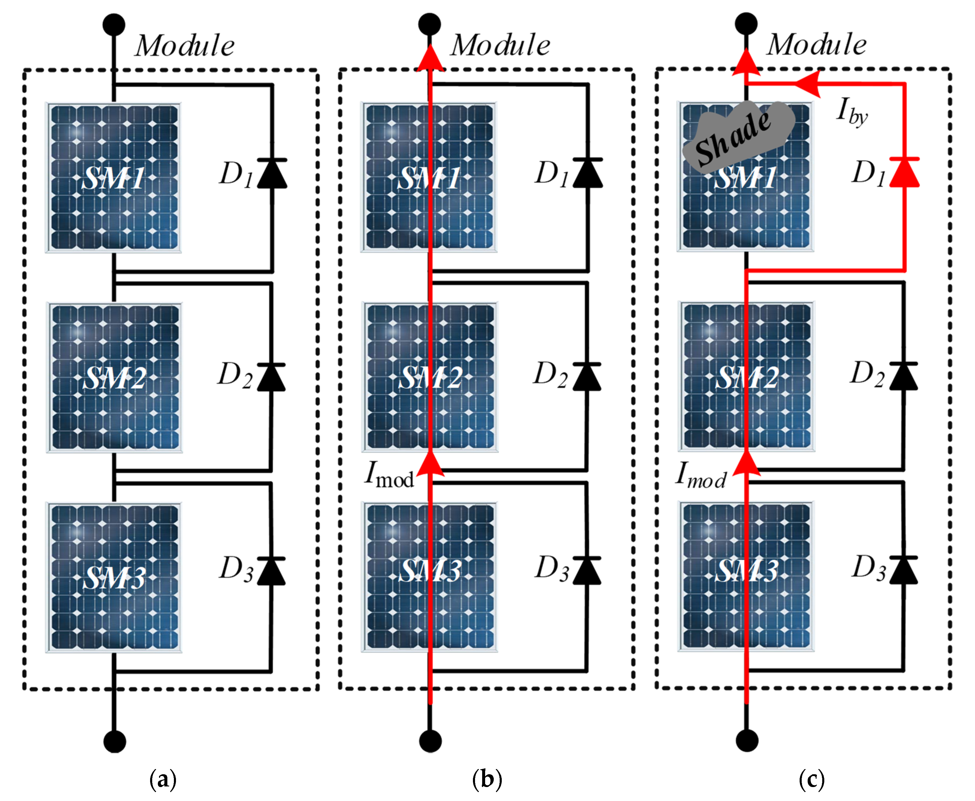
In the commercial PV modules, a parallel-connected bypass diode is installed with each submodule, as shown in Figure 1a. This bypass diode reduces the mismatch effect under partial shading or other non-idealities, which are discussed above. When there is no mismatch, bypass diodes remain OFF and the same current Imod conducts through all submodules, as depicted in Figure 1b. If a mismatch occurs, the parallel-connected bypass diode turns ON due to the appearance of a negative voltage across the shaded PV submodule, and this shaded PV submodule is bypassed by that ON-state diode, as exemplified in Figure 1c. A current Iby starts to flow through this bypass diode. However, the bypassed submodule causes a voltage mismatch, which results in several power peaks. Hence, the conventional maximum power point tracking (MPPT) algorithms are generally unable to distinguish between local and global maxima in the power-voltage (P-V) curve of PV systems, which also impacts the performance of the whole PV system. Therefore, global maximum power point tracking (GMPPT) algorithms are required to identify the global peak [15,16,17,18,19].
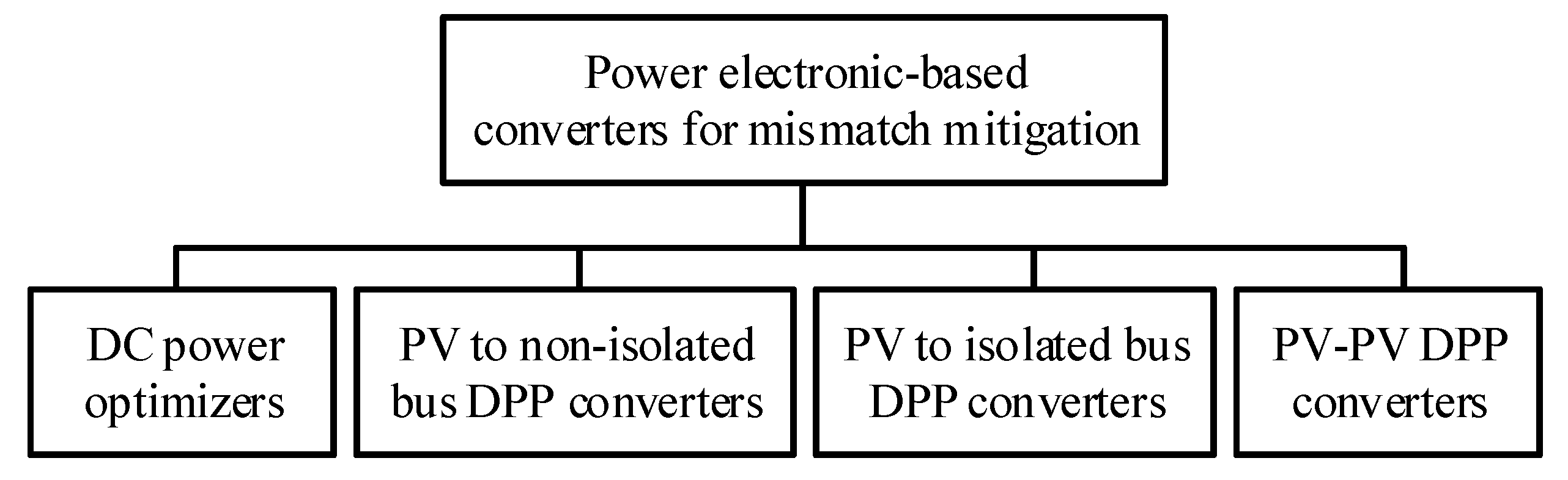
Recently, active mismatch mitigation techniques based on power electronics have been developed for PV systems, as categorized in Figure 2 [20,21,22,23,24,25,26]. In Figure 2, the distributed maximum power point tracking (DMPPT) systems, which consist of micro-converters, have been developed to resolve the mismatch problems [27,28,29]. In the DMPPT, submodules are controlled individually, and DC power optimizers are the most common example. In DC power optimizers, all submodules operate at their respective MPPs if these DC optimizers are applied at the sub-module level. However, they require the same number of converters as the number of PV submodules, which enhances the structural complexity and the cost of the system [30]. Besides, DC optimizers process the complete amount of power instead of partially processing the mismatched power between the series-connected PV submodules. Therefore, DC optimizers increase the voltage stresses and losses over the components along with their size and cost.
In the search for a more effective solution, the differential power processing (DPP) converters are found to be a more viable solution. DPP converters usually use a ladder-based architecture, which has been previously explored in the battery voltage equalization [31,32,33], multicore CPU power delivery [34], and other PV applications [35,36,37,38]. In solar PV installations, DPP topologies have been found to be effective for the mitigation of the mismatch effects. When DPP converters are compared to the other power electronic-based solutions, these converters process only a fraction of power known as mismatched power. There exist a few DPP-based architectures in the literature [39,40,41] and these architectures are commonly divided into three categories, i.e., (a) PV to the non-isolated bus [37,42], (b) PV to the isolated bus [37,43], and (c) PV-PV DPP converters [37,42], as presented in Figure 2.
- (a)
- In the first category [37,42], the secondary sides of the central inverter and the DC bus are connected in parallel and they share the same voltage. Furthermore, the switching devices on the secondary side of the module-level DC-DC converter experience high voltage stress, as the DC-bus voltage is the summation of all the PV module output voltages [44].
- (b)
- The second category [37,43], which is known as an isolated bus, is formed by connecting the secondary ports of DC-DC converters in parallel. The selection of DC-bus voltage in PV to an isolated bus DPP converter topology enhances the complexity of the design, as it can be selected independently from the PV module voltage. Also, in (a) and (b), the size and power loss increase due to the presence of more components along with the cost.
- (c)
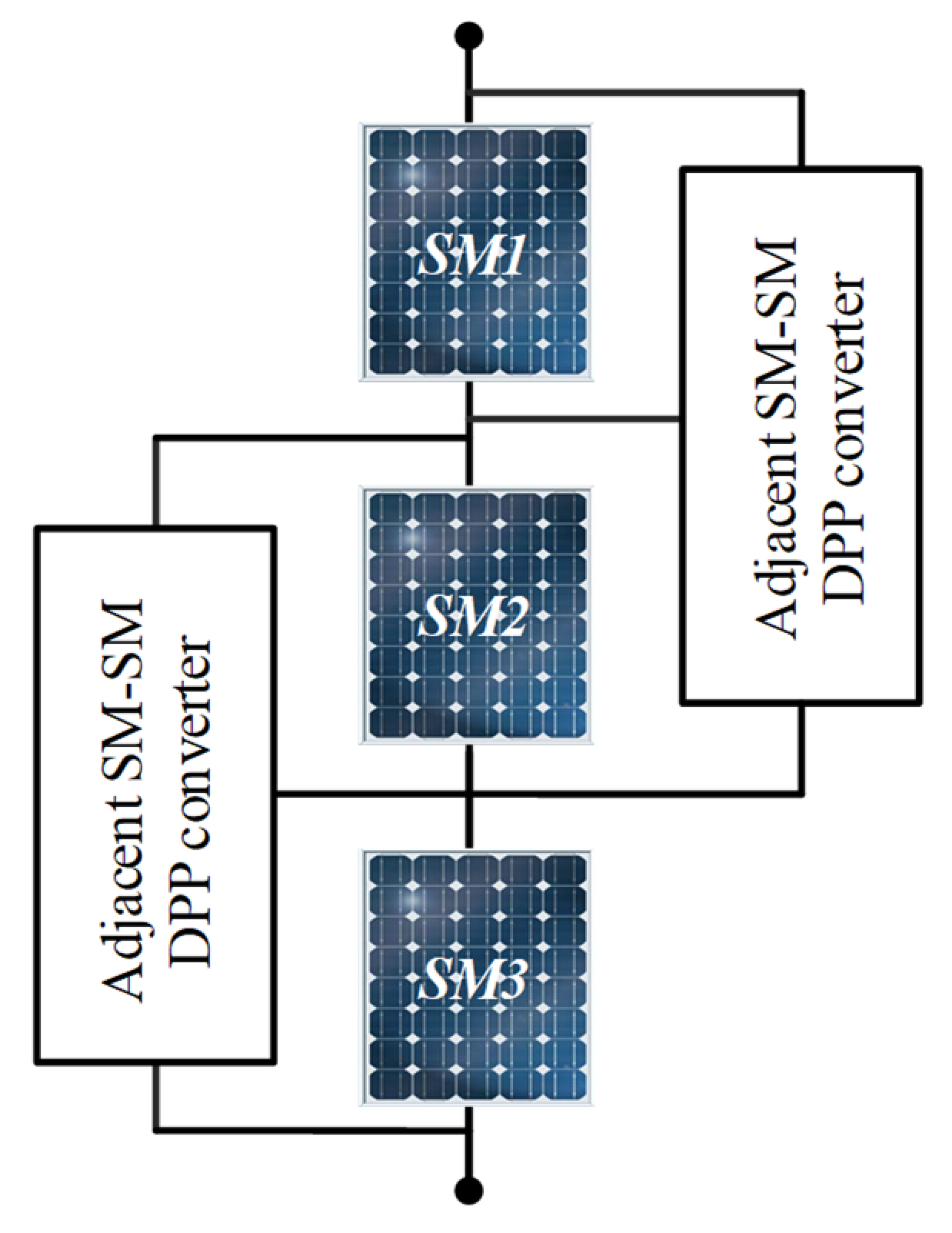
- Lastly, the third DPP, which is known as the PV-PV DPP converter [42,45] are non-isolated DPP architectures, which can be built cost-effectively through modular combinations. These PV-PV DPP converters draw power from adjacent PV modules. The general structure of PV-PV DPP is shown in Figure 3. Moreover, this topology has one less power converter than the number of PV modules, i.e., one less PV-PV DPP converters is required than the total number of PV modules. The main benefit of this architecture is that its converters are designed according to the voltage characteristics of the PV module rather than that of the main bus voltage. Therefore, the PV-PV DPP converter is independent of bus voltage and need not withstand the high voltage stresses. PV-PV DPP converters are emerging DPP topologies, which are improving continuously in terms of performance, cost, and reliability [42,46].
In continuation, many attractive PV-PV DPP topologies are presented in the literature, i.e., energy recovery [47], buck-boost [35,48], and switched-capacitor (SC) topologies [45,49,50,51]. For PV module-level applications, these DPP converters encounter several challenges such as high power conversion loss, voltage equalization, scalability, control structures, performance under severe mismatch (cell(s) or sub-module(s) that are completely blocked or there is irradiance difference between the shaded and non-shaded PV cells or sub-modules are around 70–80%) [7], and increased circuit component voltage stresses [46].
To overcome mismatch issues in the PV system, a simple concept based on a switched-capacitor-inductor (SCL) is presented in this paper. The initial work containing the proposed concept was published in [52]. However, the presented circuit details and the analysis are not sufficient along with limited simulated results. Therefore, this work contains an explicit analysis along with the experimental testing to describe the operation of the SCL DPP topology. The organization of the rest of this paper is given below. A conventional and state-of-the-art mismatch mitigation method, i.e., bypass diode topology is discussed in Section 2. The major features, working principle, and the power loss analysis of the proposed SCL topology are also detailed in Section 2. Section 3 presents the simulation results, which are compared with the bypass diode. In Section 4, experimental results are provided. Finally, Section 5 presents the conclusion of the work.
2. Proposed DPP Methodology
2.1. Conventional Mismatch Mitigation Method
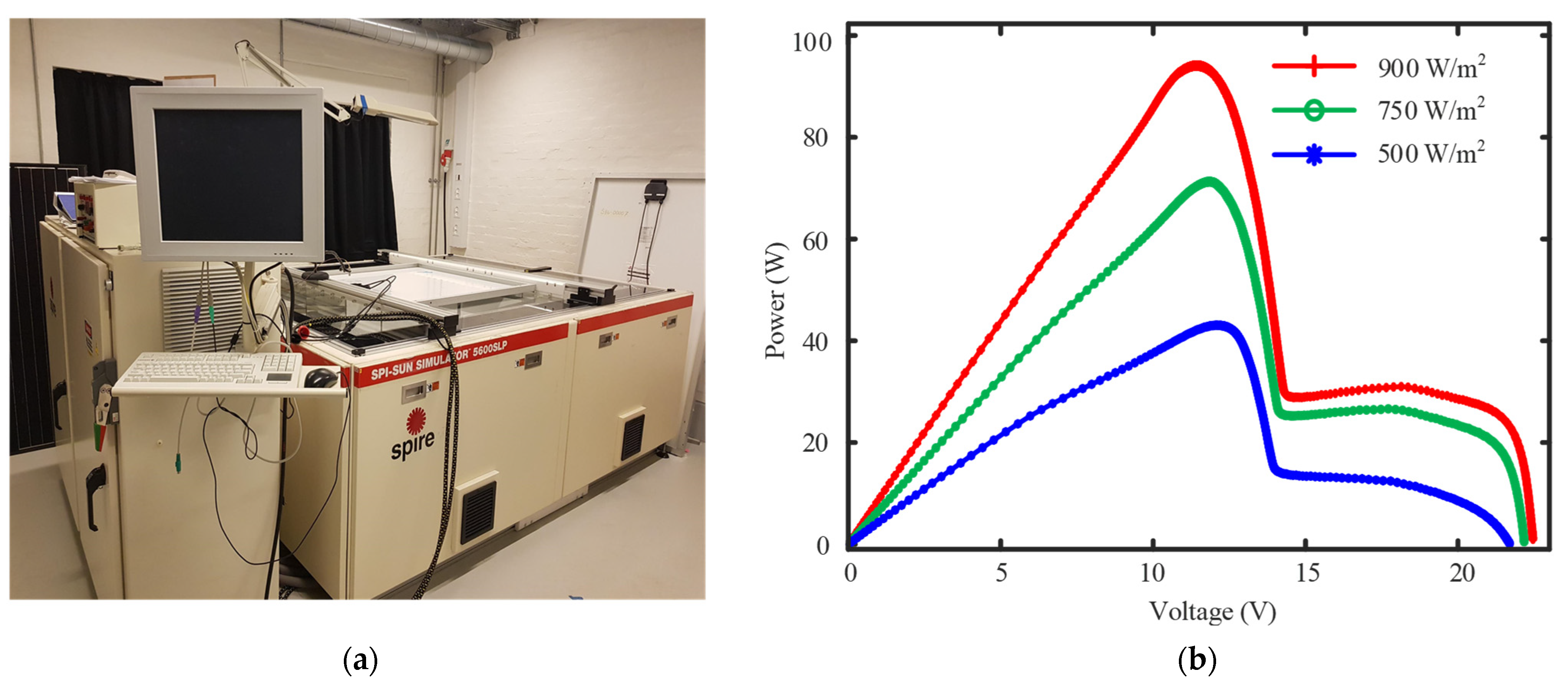
Before introducing a proposed methodology, a traditional bypass diode solution is discussed. Their pros and cons are also presented during the discussion from the perspective of the mismatch effect. For this purpose, the experimental setup and the implementation findings are shown in Figure 4. During experiments, shading over a PV module is induced to create a mismatch by covering one of the cells from the 36 cells PV module shown in Figure 4a. Under one cell-shaded condition, the irradiance levels over the PV module are varied as 900 W/m2, 750 W/m2, and 500 W/m2. The P-V characteristics are obtained under these conditions, which is shown in Figure 4b. As observed in Figure 4b, the output power is reduced due to the bypassing of a submodule, which shows that the shading over a single PV cell can cause a bypassing of the whole PV sub-module, which consists of 12 series-connected PV cells. Additionally, the bypassed submodule has no contribution to the output power and the overall 150 W PV module has lost around 33% of its power due to shading over one PV cell when irradiance over the module is 900 W/m2. Therefore, it is highly desirable to extract the lost energy. Furthermore, the bypassed submodule becomes a cause of multiple power peaks due to the partial shading. Therefore, the proposed DPP technique is employed to extract the lost power due to the bypass diode method that is highlighted in the subsequent sections.
2.2. Main Features and Qualitative Comparison with Other DPP Converter Topologies
There are many attractive PV-PV DPP topologies mentioned in Section 1 from the literature, i.e., energy recovery [47], buck-boost [35,48], and SC [45,49,50,51]. For PV module-level applications, these DPP converters encounter several challenges such as high power conversion loss, voltage-equalization, scalability, control structures, performance under severe mismatch, and increased circuit component voltage stresses. For example, the energy recovery DPP topology [47] is suitable only for simple shading scenarios. Moreover, this topology has high power electronic conversion losses along with a large number of power electronic components. Besides, the complex control circuitry is also required to drive the active components in the energy recovery DPP topology. Another DPP topology, which is known as buck-boost topology, is presented in [35], which shows a significant performance degradation in the circumstances of higher levels of mismatch. Also, the switches have to stand with large voltage stresses (twice the proposed converter) in buck-boost DPP topology, which affects the long-term reliability of the active components. Therefore, switches with a high voltage rating are required for buck-boost DPP topology, which increases the size and price of the topology.
In continuation, the ladder-based SC DPP topologies are one of the most famous members of the adjacent PV-PV DPP class. In SC, the number of PV modules can be extended easily through modularly inter-connecting switches and capacitors. Many SC-based DPP topologies are presented in the literature [53,54,55]. Usually, the existed SC-based DPP topologies use additional active devices to process the mismatched power, especially during severe mismatch by introducing more switching states. These switching states make the control circuitry more complex. The most common SC topologies are resonant SC (RSC) [49], RSC gyrator [54,56], and simple SC [45]. In the RSC-based DPP topology [49], there are three modes of operation. Firstly, the resonant tank is charged while it discharges in the second mode of operation to release the energy that comes from a mismatch between series-connected PVs. Finally, in the last mode of operation, a short circuit is applied within the resonant tank to induce the requisite charge balance by discharging the residual energy. Notably, the operating switching sequences are important to obtain the desired output, which makes the circuit complex to control. Another SC-based DPP topology is presented in [22], which uses one inductor for four modules. Even when using one inductor, the circuit needs a high count of switching devices and diodes, i.e., for a system consisting of four series-connected PV modules, 8 switches and 10 diodes are required. Furthermore, during the charging and discharging phase of an inductor, only one combination of switches and diodes can work. Therefore, the optimal switching sequence has to be sought to extract MPP for non-ideal conditions (partial shading). During this process, the search for the most favorable switching state becomes difficult in several cases, which increases the computational time and control complexity. Therefore, effective tracking could not be guaranteed in rapidly changing environmental conditions. In order to overcome some of the challenges faced by existing DPP converters, the SCL-based DPP topology was proposed. This topology was derived from buck-boost and SC-based DPP topologies. Compared to buck-boost and SC-based DPP topologies, the proposed SCL topology has the following features:
- a better performance under severe mismatching,
- less inductor current ripple,
- simple control circuitry, and
- equalization of the series-connected PV submodule voltages.
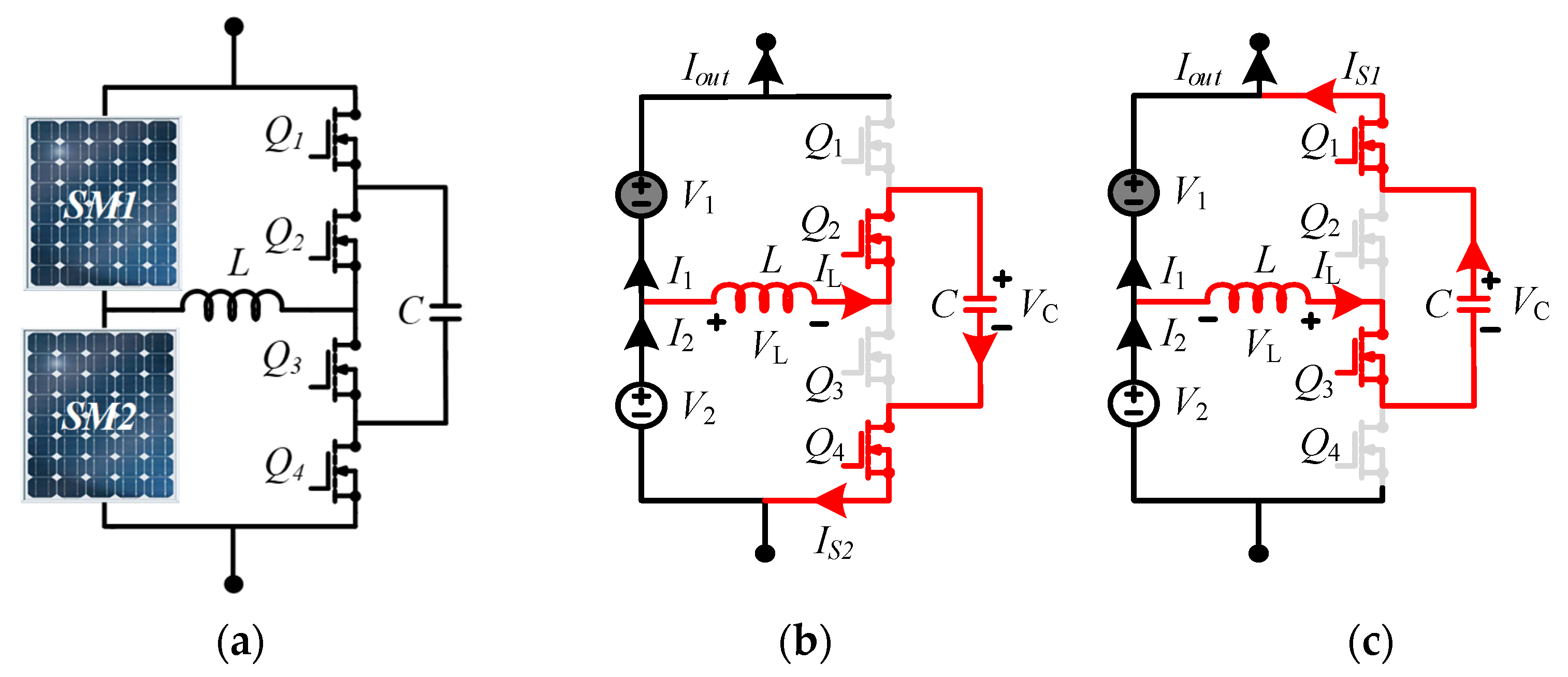
2.3. Operational Analysis
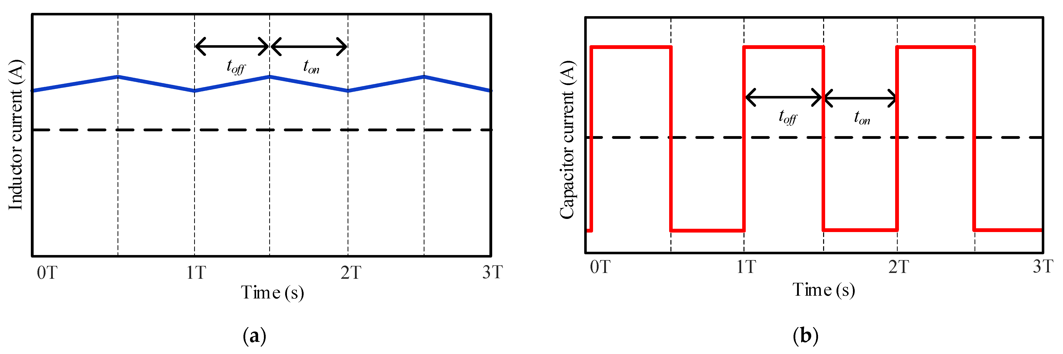
The proposed topology has a ladder-based PV-PV architecture (see Figure 5). In this topology, a mismatched power is processed by the switched-capacitor C and inductor L. The SCL DPP topology has two operational modes and their equivalent circuits are depicted in Figure 5b,c. Four MOSFET devices (Q1~4) are used during the operation, which is operating at a high frequency to distribute the mismatch charges equally between the submodules. These MOSFET devices are switched at a duty cycle of 50%. During the first cycle, Q1 and Q3 are switched OFF by keeping Q2 and Q4 in an ON-state, as demonstrated in Figure 5b. In the next cycle, the transistors Q1 and Q3 are switched ON while Q2 and Q4 are switched OFF, as shown in Figure 5c. The difference of the currents named as the mismatched current IL flows across the inductor L. The value of the current IL is maintained by the inductor L, which is represented in Figure 6a. Furthermore, the mismatch charges between SM1 and SM2 are distributed by the capacitor C in a way that the equalization of voltages is achieved at a submodule level with the proposed topology. Moreover, switching at a higher frequency allows maintaining the constant voltage on capacitor C. Additionally, the capacitor current is also shown in Figure 6b.
To further explain the operational principle of the proposed topology, a shade is applied on the submodule to induce the mismatch, as shown in Figure 5. Firstly, PV submodules are producing the same amount of energy. Hence, no mismatch power is processed by the converter. Now, if there is a power mismatch between SM1 and SM2, as shown in Figure 5, the proposed DPP converter starts to process and distributes the mismatched power between adjacent series-connected PV submodules through constant charging and discharging of the capacitor C. The schematic diagram of the equivalent SCL topology during mismatch is shown in Figure 5b,c, where voltages across SM1 and SM2 are represented as V1 and V2, respectively. Considering the scenario of partial shading at SM1, the switching sequence and the associated equivalent circuit of the DPP converter are presented in Figure 5b,c. In the case when Q2 and Q4 are switched ON (Q1 and Q3 OFF), corresponding to Figure 5b, the differential current IL passes and charges the inductor L and a capacitor C. The voltage across the capacitor VC and the current I2 flowing across SM2 can be mathematically represented by Equations (1) and (2) as below:
where IL is the mismatch current flowing across the inductor L, V2 is the voltage across the SM2, L is the value of the inductance, VC is the voltage across the switched-capacitor, and I1 is the current flowing across SM1.
In the next cycle, which is shown in Figure 5c, Q1 and Q3 are turned ON while keeping Q2 and Q4 in an OFF-state. In this scenario, the capacitor voltage VC and the current passing through SM2 can be represented by (3) and (4)
where V1 is the voltage across the SM1.
Since the duty cycle for the proposed SCL-based DPP topology is fixed at 50%, the average mismatch inductor current IL is distributed equally into IS1 and IS2 (currents flowing through Q1, Q2, Q3, and Q4). The current following through the output and switches can be found by using (5) and (6).
where Iout is the current flowing towards the output load.
2.4. Component Design
In general, there is a direct relationship between the inductor losses and the root-mean-square (RMS) inductor current ripple ΔIL. A high RMS current ripple results in a high-frequency RMS flux density and hence substantial core losses [57,58]. Furthermore, a high RMS current ripple (should be less than 5%) causes a high-frequency copper loss due to proximity and the skin effect. Therefore, the inductor current ripple ΔIL is a reasonable performance indicator for the design of the inductor, which should be as small as possible. On the other hand, the capacitance value should be large enough to limit the DC voltage ripple ΔVC to less than 5%. The inductance and capacitance can be calculated as
where fsw is the switching frequency.
2.5. Power Loss Analysis
The loss of the DPP converter is briefly evaluated. The major power loss encountered in the proposed topology includes: (a) switching losses, (b) conduction losses, (c) losses in energy storage devices, and (d) leakage losses. Leakage losses are very small and therefore have been ignored in the analysis. Alternatively, remaining losses have been used to evaluate the performance of the proposed DPP. Firstly, the ON-state power loss (Pon) for the switches in the proposed topology can be calculated by
where Ron is the ON-state resistance of the MOSFETs and ISi(RMS) (i = 1 or 2) is the RMS value of mismatch current flowing across the switches while the switch is in an ON-state. In each cycle, two MOSFETs are ON. Therefore, the ON-state losses are multiplied by a factor of 2.
A higher switching frequency fsw reduces the capacitor and inductor sizes. However, it enhances the switching losses [40]. At any switching instance, since two switches are involved, switching power losses (Pswloss) can be estimated as (10)
where iSi(tsw_on) is the instantaneous MOSFET current during the turn-ON, iSi(tsw_off) is the current during the turn-OFF, and ton and toff are the rise and fall time of the switch, which are mentioned in the datasheet.
It can be seen from Figure 5 that IL always flows through L and C. Firstly, power losses of the inductor can be determined with the inductor’s current (IL(RMS)) and the inductor copper resistance RL at fsw. For the inductor L, the copper losses (PL_loss) can be computed as
Once L is designed, the capacitor C is designed to be large enough for better charge distribution during mismatch. Similarly, for a capacitor C, the power losses (PC_loss) can be calculated by
where RC(fsw) is the effective series resistance of C at fsw.
Consequently, the overall power losses can be found by summing up all the losses in (9)–(12), which are given as
where Pt is the total power loss.
The overall loss evaluation for the proposed SCL-based DPP topology has been performed using (9)–(13), and the findings have been discussed in the subsequent sections.
3. Simulation Results
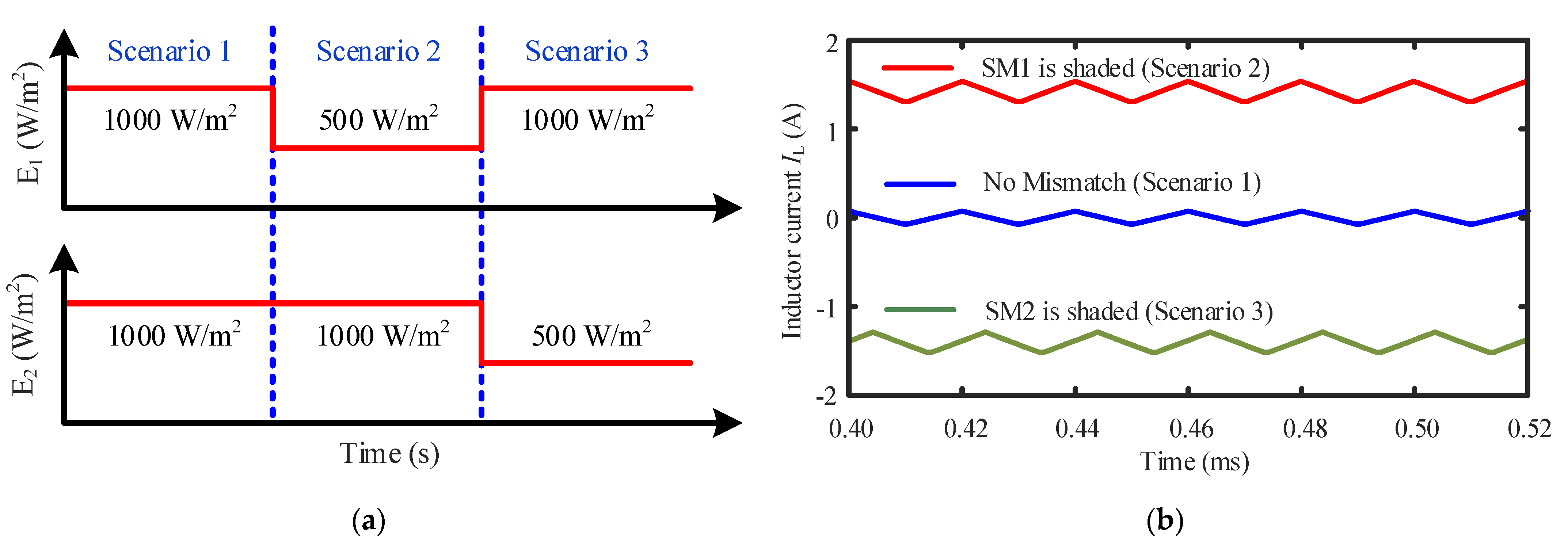
For the performance evaluation of the proposed SCL-based DPP topology, simulations are performed under various mismatch scenarios shown in Figure 7a. These mismatch cases are developed by varying the irradiance over the PV modules, i.e., E1 for SM1 and E2 for SM2. The rating of the used PV module is shown in Table 1. The converter is operating at a 50% duty cycle and the operating frequency is 100 kHz. The value of inductor L and a capacitor C are 100 µH and 50 µF, respectively by taking a consideration of the inductor current ripple ΔIL and capacitor voltage ripple ΔVC to be less than 5% according to (7) and (8).
- Scenario 1—No shading
During this scenario, there is no shading, SM1 and SM2 are producing the same amount of power. Therefore, the mismatch current IL between SM1 and SM2 is negligible, which can be seen from Figure 7b.
- Scenario 2—SM1 is shaded
The irradiance over SM1 is reduced to 500 W/m2, while it remains constant over SM2 to 1000 W/m2 during this scenario. The simulation results are given in Figure 7b. In Figure 7b, the mismatch current IL is passing through the inductor. An average mismatch current is around 1.4 A.
- Scenario 3—SM2 is shaded
In this scenario, the irradiance over SM2 is reduced to 500 W/m2 while it remains constant over SM1 to 1000 W/m2. The simulation results are shown in Figure 7b.
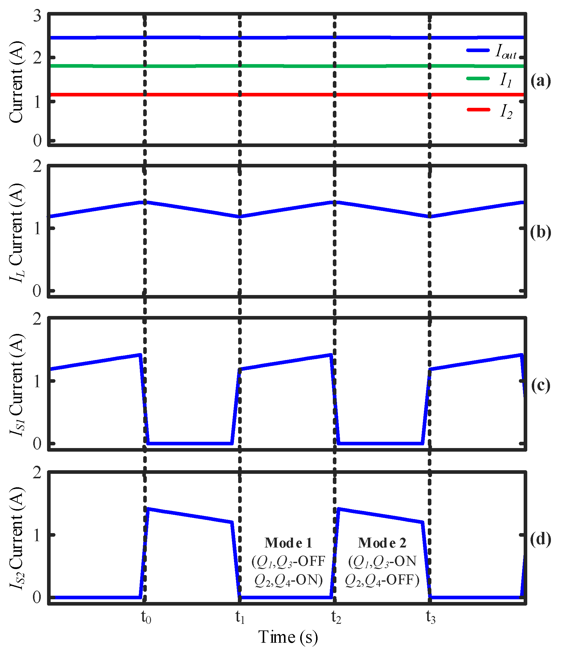
To further explain the operation of the proposed SCL-based topology, simulated results under scenario 2 are presented in Figure 8. In Figure 8, the current is flowing towards the output load (Iout) and PV modules (I1 and I2) in Figure 8a, inductor L (IL) in Figure 8b, and MOSFET switches (IS1 and IS2) in Figure 8c,d during both operational states. For further assessment and evaluation, the performance of the SCL methodology in Figure 5 is compared with the conventional bypass diode method in Figure 1. For this purpose, several cases are developed and performed in PSIM, which are given in Table 2.
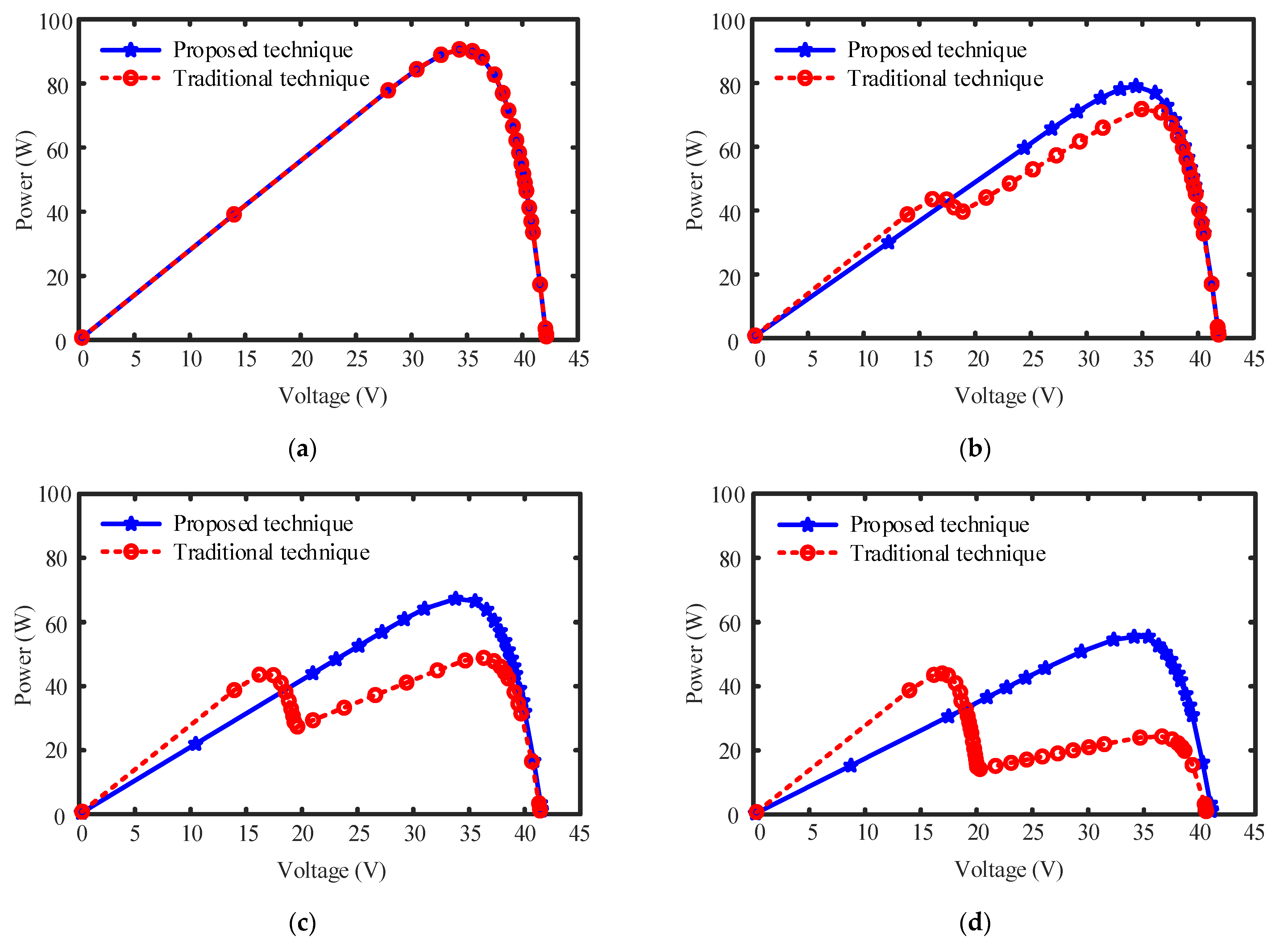
The simulation results are presented in Figure 9 and Figure 10 for the traditional bypass diode and SCL-based DPP topology. In Figure 9, the P-V characteristics are shown under different mismatch cases. These mismatch cases are given in Table 2 by varying the irradiance (E1) over SM1 (1000 W/m2, 750 W/m2, 500 W/m2, and 250 W/m2) while keeping the irradiance (E2) over SM2 constant (i.e., 1000 W/m2) in Figure 5. In Figure 9, under these mismatch conditions, the proposed SCL-based DPP topology has achieved only one power peak while there are multiple peaks by using the conventional bypass diode method, as shown in Figure 9b–d.
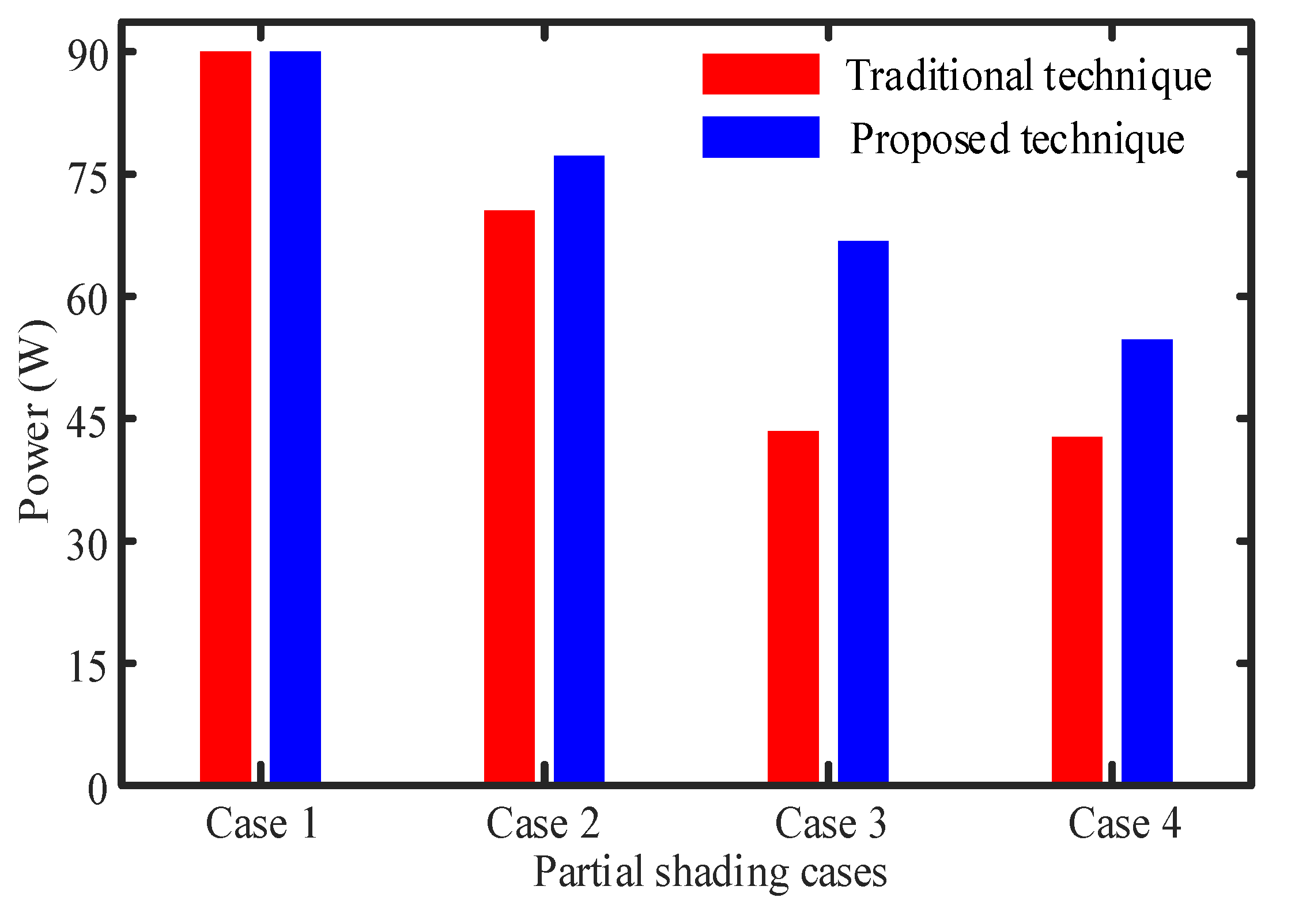
In Figure 10, the maximum output power achieved from the proposed DPP topology and conventional bypass diode is shown. It is shown that the power achieved by using the proposed DPP is greater than using the traditional bypassing diode methodology during various mismatch cases mentioned in Table 2. Moreover, energy yield by the conventional bypass diode method during the mismatch cases 3 and 4 is similar (~45 W) and is significantly lower than the proposed DPP topology. During these cases, the conventional bypass diode method bypasses the low power-producing PV submodule. Therefore, the power is not fully extracted by the bypass diode methodology, but it is effectively extracted by the proposed SCL DPP topology. Overall, the results in Figure 9 and Figure 10 have confirmed the effectiveness of the proposed DPP topology under non-ideal situations. Moreover, PV submodule voltages are also given in Table 3 under the similar mismatch conditions mentioned in Table 2. It may be observed that the proposed topology has equalized the voltages during all the mismatch cases. Therefore, the proposed topology requires a simple MPPT tracking algorithm.
4. Experimental Results and Discussion
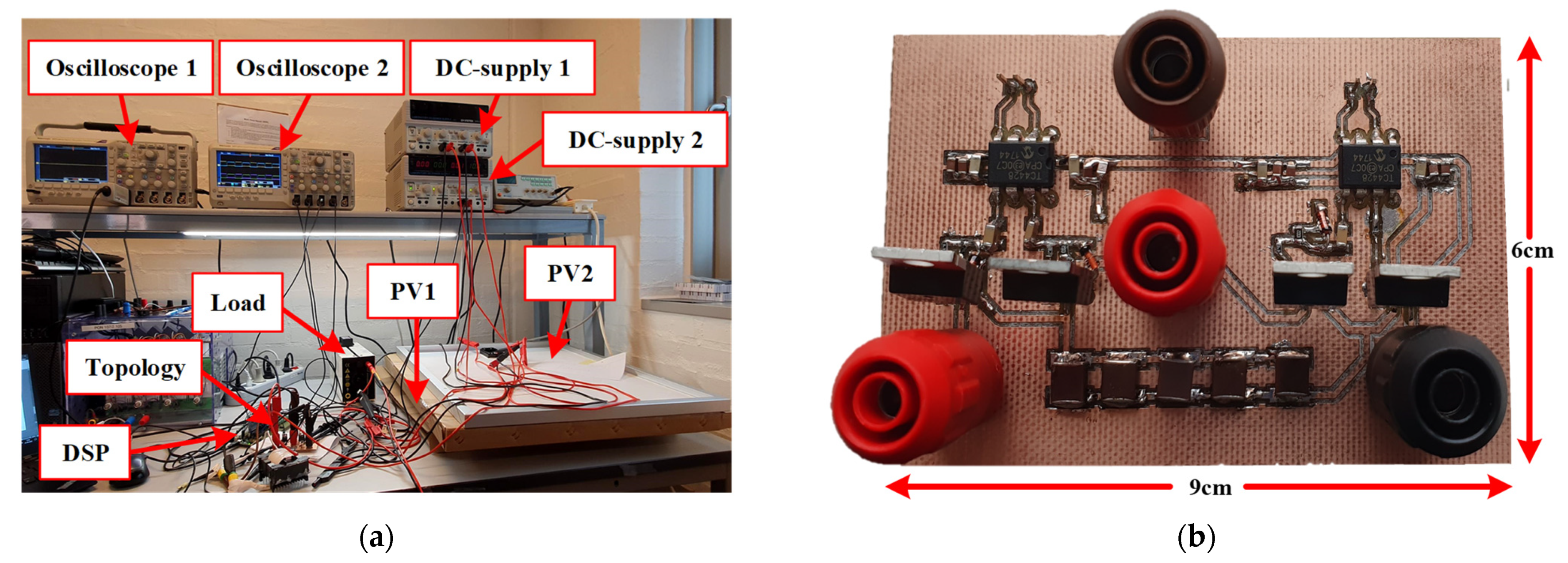
4.1. Prototype and Experimental Setup
The prototype along with the experimental setup is presented in this section. For experimental validations, two solar PV modules (PV1 and PV2) are used. The prototype of 100 W is designed by considering the 45 W PV module to test it within a laboratory environment. The rating of PV modules used for hardware implementation is shown in Table 1. The parameters and components used for the experimental setup are listed in Table 4. In Table 4, the values of inductor L and a capacitor C are shown to be 100 µH and 50 µF, respectively by taking a consideration of the inductor current ripple ΔIL and capacitor voltage ripple ΔVC of less than 5% according to (7) and (8). Moreover, the proposed DPP converter only has to process the mismatched power. Therefore, the power rating requirement for the proposed DPP converter is lower. Hence, the low power components allow the use of small and fast-switching MOSFET transistors, which can operate at high switching frequencies. The inductance, capacitance, and switching frequency values were determined earlier. More importantly, this prototype is designed to prove the concept, and is not for practical use. Therefore, the components used during the testing should be replaced by the more efficient and small-size components for practical implementation.
For the experimental setup, each PV module is connected in parallel with a DC power supply, as depicted in Figure 11a. The DC supply is operating in the constant-current (CC) mode to emulate the light-induced current, depicting the output current-voltage (I–V) curve. Details about this method to conduct repeatable indoor PV experiments can be found in [59]. Through the control of constant current mode, different conditions of mismatch can be emulated. The designed prototype is shown in Figure 11b.
4.2. Results
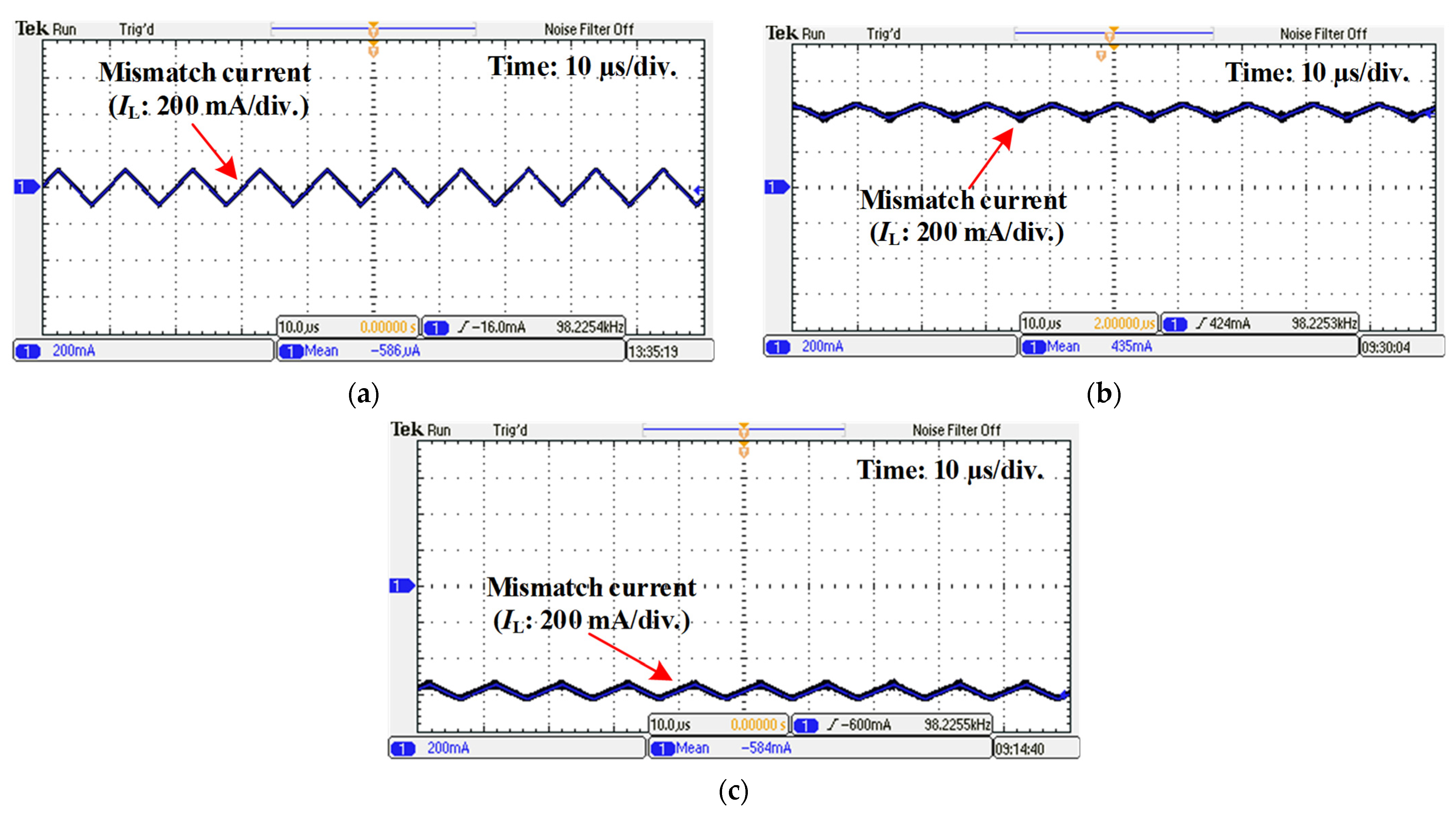
This section compromises experimental results along with the theoretical analysis of power loss distribution among different circuit components to verify the proposed work. For this purpose, three mismatch conditions are developed, which are shown in Table 5, i.e., Test 1, Test 2, and Test 3. The experimental results under these conditions are presented in Figure 12 for SCL-based DPP converters. Figure 12 shows the mismatch current process by the SCL-based DPP converters. In the first condition (Test 1), when there is no mismatch between the series-connected PV modules, the mismatch current IL is shown in Figure 12a. It can be seen from Figure 12a that the mismatch current during this test condition is zero. During Test 2, PV1 is producing more power than PV2. The mismatch current during this case is shown in Figure 12b. Lastly, in Test 3, PV2 is producing more power than PV1, while the difference of mismatch current IL between the two series-connected PV modules is shown in Figure 12c.
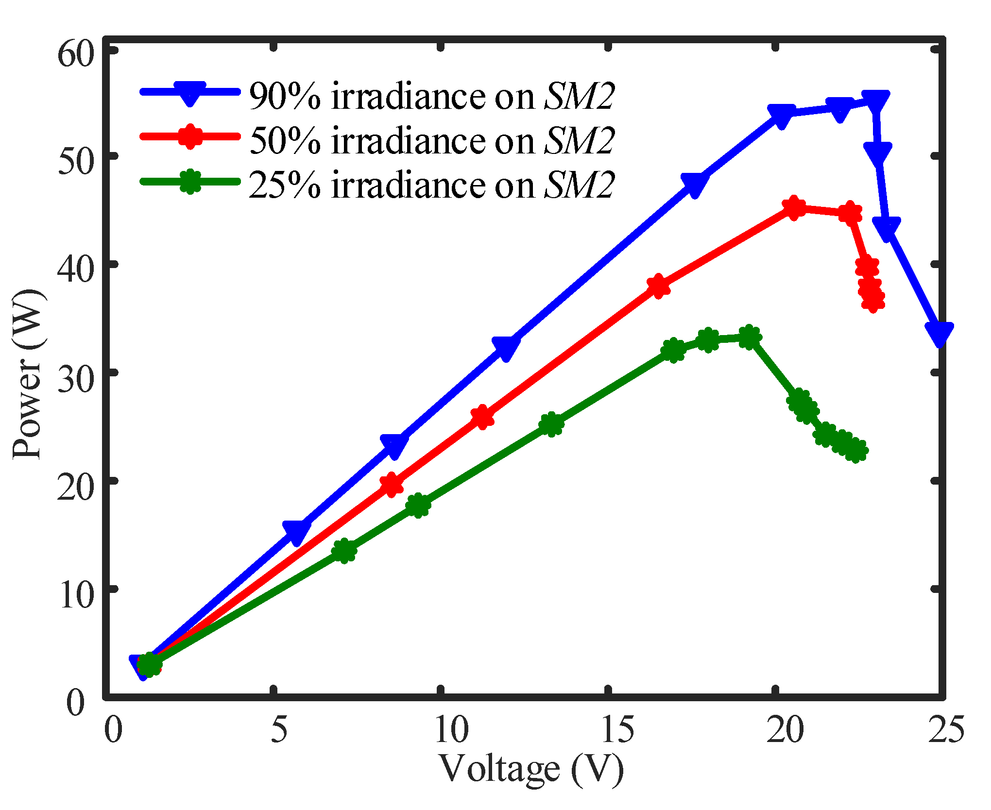
P-V characteristics for the proposed SCL topology are shown in Figure 13, which are measured by sweeping the variable load shown in Figure 11a. To measure the P-V characteristics, PV1 (30 W) is used as a reference PV module while PV2 is working at 90%, 50%, and 25% of PV1 to create a mismatch effect. It can be seen from Figure 13 that the P-V characteristics of the proposed SCL-based DPP methodology have no local maxima, as it has only one peak under all tested mismatch conditions. Hence, it becomes easy to track MPP by using simple MPPT control algorithms under partial shading or other non-ideal conditions, which causes a mismatch.
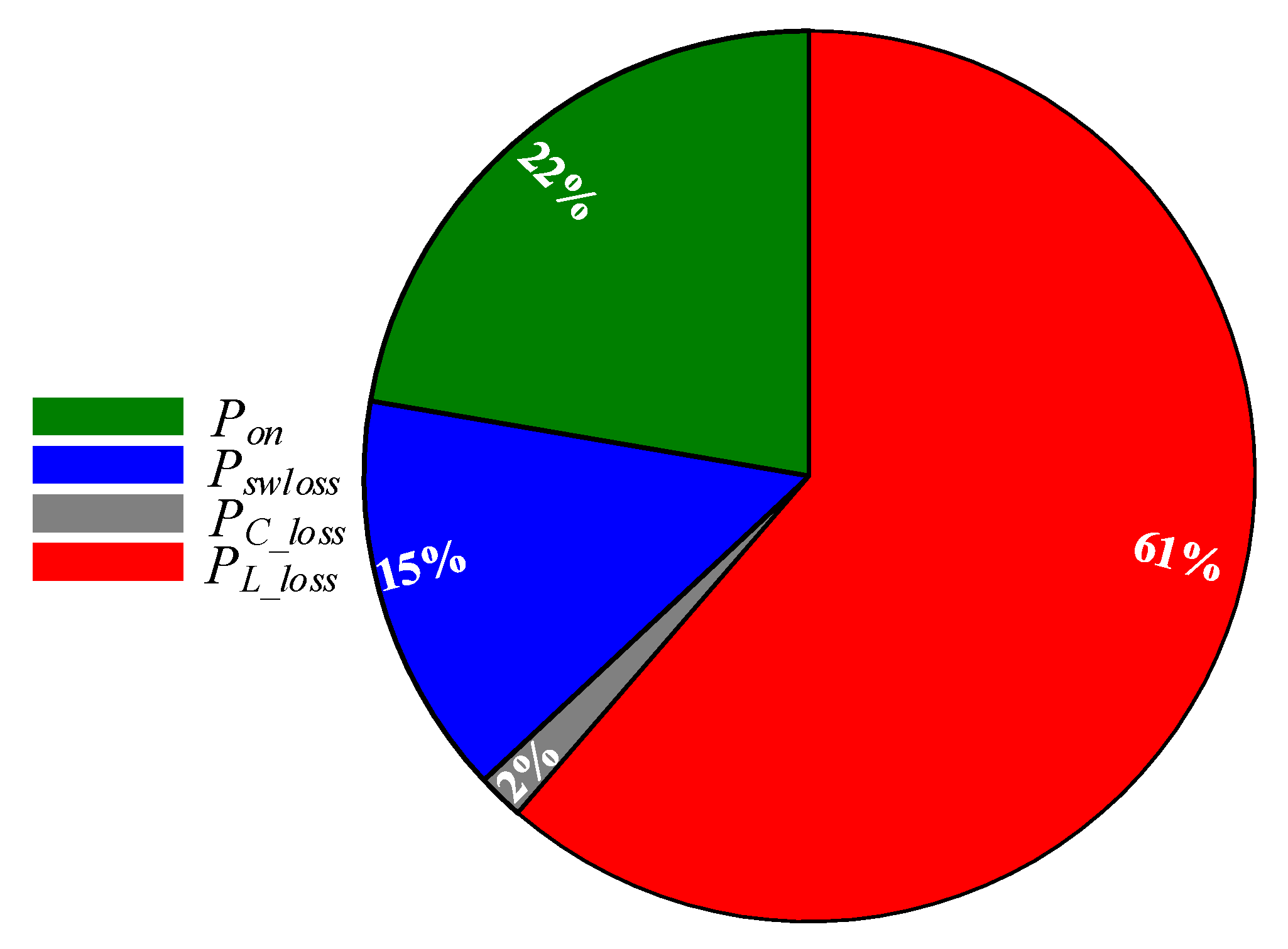
The power loss breakdown across each component for the proposed topology is presented in Table 6. The ratings of each PV submodule along with other parameters, which are used for the loss calculation are mentioned in Table 4 and Table 5, respectively. For the loss calculation, one submodule is producing half power, while the other is producing at its maximum capacity. The theoretically calculated on-state MOSFET power losses (Pon) and switching power losses (Pswloss) are 109.83 mW and 71.69 mW, respectively. Moreover, the calculated losses across the capacitor (PC_loss) and inductor (PL_loss) are 8.3 mW and 300 mW, correspondingly. The overall calculated efficiency (ƞc) is 99.28% and the measured efficiency from the simulated results under similar conditions is 98.66%. Additionally, the calculated and simulated efficiencies are only considered because this prototype is designed only to prove the concept, not for practical use. Therefore, the components used during the testing should be replaced by the more efficient and small-size components for practical implementation for better performance and efficiency. As a continuation, it can be seen from Figure 14 that the losses associated with the inductor are the highest up to 61% because the copper loss is the most dominant material showing major losses at higher frequencies. Also, the ON-state switch losses are lower due to the low Ron of the selected MOSFET.
Overall, the proposed topology is simple and has the potential to withstand non-ideal conditions by yielding the maximum power from a PV system. Moreover, the control circuitry is simple and easy to implement with only two modes of operations as compared to other complex SC topologies. Furthermore, the size of the proposed topology is compact, and thus, it is easily integrable into a PV module junction box. In a word, the proposed work has reduced the complexity and increased the output power yield with high efficiency.
5. Conclusions
A power electronic-based differential power processing (DPP) converter to mitigate the mismatch effects in solar PV modules is proposed in this paper. The proposed switched-capacitor-inductor (SCL)-based topology is based on the concept of battery voltage equalizer. The proposed work equalizes the voltages at the level of the PV submodule and makes it possible for PV submodules to operate near to their maximum power point (MPP).
For verification of the proposed topology, a simulation model was built in PSIM. Additionally, a hardware prototype was also built for the verification of the concept through experimental tests. The simulation and experimental results show that the SCL-based DPP converter overcomes the problem of multiple peaks in the output power of PV modules under various mismatch conditions by using simple control circuitry. The converter has achieved an efficiency above 98%. Moreover, the proposed DPP topology has been evaluated against the conventional traditional bypass diode. The comparison has shown that the proposed topology is simple, easy to integrate due to its small size, highly granular, reliable, and efficient even under a severe mismatch.
Author Contributions
Conceptualization, K.A.K.N. and Y.Y.; methodology, K.A.K.N. and Y.Y.; software, K.A.K.N.; validation, K.A.K.N., Y.Y. and T.K. and D.S.; writing—original draft preparation, K.A.K.N.; writing—review and editing, K.A.K.N., Y.Y. and T.K. and D.S.; visualization, K.A.K.N., Y.Y., T.K. and D.S.; supervision, Y.Y., T.K. and D.S. All authors have read and agreed to the published version of the manuscript.
Funding
This research received no external funding.
Institutional Review Board Statement
Not applicable.
Informed Consent Statement
Not applicable.
Data Availability Statement
Not applicable.
Conflicts of Interest
The authors declare no conflict of interest.
References
- Çakirlar Altuntaş, E.; Turan, S.L. Awareness of secondary school students about renewable energy sources. Renew. Energy 2018, 116, 741–748. [Google Scholar] [CrossRef]
- The International Energy Agency (IEA). 2018 Snapshot of Global Photovoltaic Markets; IEA: Paris, France, 2018. [Google Scholar]
- The International Energy Agency (IEA). 2018 Photovoltaic Module Energy Yield Measurements: Existing Approaches and Best Practice; IEA: Paris, France, 2018. [Google Scholar]
- Candelise, C.; Winskel, M.; Gross, R.J.K. The dynamics of solar PV costs and prices as a challenge for technology forecasting. Renew. Sustain. Energy Rev. 2013, 26, 96–107. [Google Scholar] [CrossRef] [Green Version]
- Dhaundiyal, A.; Atsu, D. Energy assessment of photovoltaic modules. Sol. Energy 2021, 218, 337–345. [Google Scholar] [CrossRef]
- Al-Smadi, M.K.; Mahmoud, Y.; Xiao, W. A fast and accurate approach for power losses quantification of photovoltaic power systems under partial-shading conditions. IET Renew. Power Gener. 2021, 15, 939–951. [Google Scholar] [CrossRef]
- Dolara, A.; Lazaroiu, G.C.; Leva, S.; Manzolini, G. Experimental investigation of partial shading scenarios on PV (photovoltaic) modules. Energy 2013, 55, 466–475. [Google Scholar] [CrossRef]
- Silvestre, S.; Boronat, A.; Chouder, A. Study of bypass diodes configuration on PV modules. Appl. Energy 2009, 86, 1632–1640. [Google Scholar] [CrossRef]
- Kim, K.A.; Krein, P.T. Reexamination of photovoltaic hot spotting to show inadequacy of the bypass diode. IEEE J. Photovolt. 2015, 5, 1435–1441. [Google Scholar] [CrossRef]
- Ahsan, S.; Niazi, K.A.K.; Khan, H.A.; Yang, Y. Hotspots and performance evaluation of crystalline-silicon and thin-film photovoltaic modules. Microelectron. Reliab. 2018, 88–90, 1014–1018. [Google Scholar] [CrossRef]
- Niazi, K.A.K.; Akhtar, W.; Khan, H.A.; Yang, Y.; Athar, S. Hotspot diagnosis for solar photovoltaic modules using a naive bayes classifier. Sol. Energy 2019, 190, 34–43. [Google Scholar] [CrossRef]
- Niazi, K.A.K.; Yang, Y.; Spataru, S.V.; Mutarraf, M.U.; Sera, D. Experimental Benchmarking of Partial Shading Effect on Thin-Film and Crystalline-Silicon Solar Photovoltaic Modules. In Proceedings of the 36th European Photovoltaic Solar Energy Conference and Exhibition, Marseille, France, 9–13 September 2013. [Google Scholar]
- Niazi, K.; Akhtar, W.; Khan, H.A.; Sohaib, S.; Nasir, A.K. Binary Classification of Defective Solar PV Modules Using Thermography. In Proceedings of the 2018 IEEE 7th World Conference on Photovoltaic Energy Conversion (WCPEC) (A Joint Conference of 45th IEEE PVSC, 28th PVSEC 34th EU PVSEC), Waikoloa, HI, USA, 10–15 June 2018; pp. 753–757. [Google Scholar]
- Ahsan, S.M.; Khan, H.A. Performance comparison of CdTe thin film modules with C-Si modules under low irradiance. IET Renew. Power Gener. 2019, 13, 1920–1926. [Google Scholar] [CrossRef]
- Jeon, Y.; Lee, H.; Kim, K.A.; Park, J. Least power point tracking method for photovoltaic differential power processing systems. IEEE Trans. Power Electron. 2017, 32, 1941–1951. [Google Scholar] [CrossRef]
- Sera, D.; Mathe, L.; Kerekes, T.; Spataru, S.V.; Teodorescu, R. On the perturb-and-observe and incremental conductance MPPT methods for PV systems. IEEE J. Photovolt. 2013, 3, 1070–1078. [Google Scholar] [CrossRef]
- Dolara, A.; Grimaccia, F.; Mussetta, M.; Ogliari, E.; Leva, S. An evolutionary-based MPPT algorithm for photovoltaic systems under dynamic partial shading. Appl. Sci. 2018, 8, 558. [Google Scholar] [CrossRef] [Green Version]
- Murtaza, A.; Chiaberge, M.; Spertino, F.; Boero, D.; De Giuseppe, M. A Maximum power point tracking technique based on bypass diode mechanism for PV arrays under partial shading. Energy Build. 2014, 73, 13–25. [Google Scholar] [CrossRef]
- Belhachat, F.; Larbes, C. A review of global maximum power point tracking techniques of photovoltaic system under partial shading conditions. Renew. Sustain. Energy Rev. 2018, 92, 513–553. [Google Scholar] [CrossRef]
- Kesarwani, K.; Stauth, J.T. A Comparative Theoretical Analysis of Distributed Ladder Converters for Sub-Module PV Energy Optimization. In Proceedings of the 2012 IEEE 13th Workshop on Control and Modeling for Power Electronics (COMPEL), Kyoto, Japan, 10–13 June 2012; pp. 1–6. [Google Scholar]
- Bergveld, H.J.; Büthker, D.; Castello, C.; Doorn, T.; de Jong, A.; van Otten, R.; de Waal, K. Module-level DC/DC conversion for photovoltaic systems: The Delta-conversion concept. IEEE Trans. Power Electron. 2013, 28, 2005–2013. [Google Scholar] [CrossRef]
- Lavado Villa, L.F.; Ho, T.-P.; Crebier, J.-C.; Raison, B. A power electronics equalizer application for partially shaded photovoltaic modules. IEEE Trans. Ind. Electron. 2013, 60, 1179–1190. [Google Scholar] [CrossRef]
- Olalla, C.; Clement, D.; Rodriguez, M.; Maksimovic, D. Architectures and control of submodule integrated DC–DC converters for photovoltaic applications. IEEE Trans. Power Electron. 2013, 28, 2980–2997. [Google Scholar] [CrossRef]
- Khan, O.; Xiao, W. Review and qualitative analysis of submodule-level distributed power electronic solutions in PV power systems. Renew. Sustain. Energy Rev. 2017, 76, 516–528. [Google Scholar] [CrossRef]
- Chu, G.; Wen, H. A Reliability Assessment of Submodule-Level Distributed Power Electronic Solution in Photovoltaic Generation System. In Proceedings of the 2020 IEEE 9th International Power Electronics and Motion Control Conference (IPEMC2020-ECCE Asia), Nanjing, China, 31 May–3 June 2020; pp. 1740–1745. [Google Scholar]
- Artal-Sevil, J.S.; Bernal-Ruiz, C.; Anzola, J.; Aizpuru, I.; Bono-Nuez, A.; Sanz-Alcaine, J.M. Partial Power Processing Architecture Applied to a Battery Energy Storage System. In Proceedings of the 2020 IEEE Vehicle Power and Propulsion Conference (VPPC), Gijón, Spain, 26–29 October 2020; pp. 1–6. [Google Scholar]
- Xiao, W.; Ozog, N.; Dunford, W.G. Topology study of photovoltaic interface for maximum power point tracking. IEEE Trans. Ind. Electron. 2007, 54, 1696–1704. [Google Scholar] [CrossRef]
- Walker, G.R.; Sernia, P.C. Cascaded DC-DC converter connection of photovoltaic modules. IEEE Trans. Power Electron. 2004, 19, 1130–1139. [Google Scholar] [CrossRef]
- MacAlpine, S.M.; Erickson, R.W.; Brandemuehl, M.J. Characterization of power optimizer potential to increase energy capture in photovoltaic systems operating under nonuniform conditions. IEEE Trans. Power Electron. 2013, 28, 2936–2945. [Google Scholar] [CrossRef]
- Ramli, M.Z.; Salam, Z. Performance evaluation of Dc power optimizer (DCPO) for photovoltaic (PV) system during partial shading. Renew. Energy 2019, 139, 1336–1354. [Google Scholar] [CrossRef]
- Lee, Y.-S.; Cheng, M.-W. Intelligent control battery equalization for series connected lithium-ion battery strings. IEEE Trans. Ind. Electron. 2005, 52, 1297–1307. [Google Scholar] [CrossRef]
- Pascual, C.; Krein, P.T. Switched Capacitor System for Automatic Series Battery Equalization. In Proceedings of the APEC 97-Applied Power Electronics Conference, Atlanta, GA, USA, 23–27 February 1997; Volume 2, pp. 848–854. [Google Scholar]
- Tahmasbi-Fard, M.; Tarafdar-Hagh, M.; Pourpayam, S.; Haghrah, A. A voltage equalizer circuit to reduce partial shading effect in photovoltaic string. IEEE J. Photovolt. 2018, 8, 1102–1109. [Google Scholar] [CrossRef]
- Zhang, S.; Tu, J.S.; Shanbhag, N.R.; Krein, P.T. A 0.79 PJ/K-Gate, 83% efficient unified core and voltage regulator architecture for sub/near-threshold operation in 130 Nm CMOS. IEEE J. Solid-State Circuits 2014, 49, 2644–2657. [Google Scholar] [CrossRef]
- Shimizu, T.; Hirakata, M.; Kamezawa, T.; Watanabe, H. Generation control circuit for photovoltaic modules. IEEE Trans. Power Electron. 2001, 16, 293–300. [Google Scholar] [CrossRef] [Green Version]
- Shimizu, T.; Hashimoto, O.; Kimura, G. A novel high-performance utility-interactive photovoltaic inverter system. IEEE Trans. Power Electron. 2003, 18, 704–711. [Google Scholar] [CrossRef] [Green Version]
- Shenoy, P.S.; Kim, K.A.; Johnson, B.B.; Krein, P.T. Differential Power processing for increased energy production and reliability of photovoltaic systems. IEEE Trans. Power Electron. 2013, 28, 2968–2979. [Google Scholar] [CrossRef]
- Niazi, K.; Khan, H.A.; Amir, F. Hot-spot reduction and shade loss minimization in crystalline-silicon solar panels. J. Renew. Sustain. Energy 2018, 10, 033506. [Google Scholar] [CrossRef]
- Anzola, J.; Aizpuru, I.; Arruti, A. Partial power processing based converter for electric vehicle fast charging stations. Electronics 2021, 10, 260. [Google Scholar] [CrossRef]
- Mellit, A.; Tina, G.M.; Kalogirou, S.A. Fault detection and diagnosis methods for photovoltaic systems: A review. Renew. Sustain. Energy Rev. 2018, 91, 1–17. [Google Scholar] [CrossRef]
- Uno, M.; Shinohara, T. Module-integrated converter based on cascaded quasi-z-source inverter with differential power processing capability for photovoltaic panels under partial shading. IEEE Trans. Power Electron. 2019, 34, 11553–11565. [Google Scholar] [CrossRef]
- Jeong, H.; Lee, H.; Liu, Y.-C.; Kim, K.A. Review of differential power processing converter techniques for photovoltaic applications. IEEE Trans. Energy Convers. 2019, 34, 351–360. [Google Scholar] [CrossRef]
- Chu, G.; Wen, H.; Jiang, L.; Hu, Y.; Li, X. Bidirectional Flyback based isolated-port submodule differential power processing optimizer for photovoltaic applications. Sol. Energy 2017, 158, 929–940. [Google Scholar] [CrossRef] [Green Version]
- Uno, M.; Shinohara, T.; Saito, Y.; Kukita, A. Review, comparison, and proposal for PWM converters integrating differential power processing converter for small exploration rovers. Energies 2019, 12, 1919. [Google Scholar] [CrossRef] [Green Version]
- Gokdag, M.; Akbaba, M.; Gulbudak, O. Switched-capacitor converter for PV modules under partial shading and mismatch conditions. Sol. Energy 2018, 170, 723–731. [Google Scholar] [CrossRef]
- Niazi, K.A.K.; Yang, Y.; Sera, D. Review of mismatch mitigation techniques for PV modules. IET Renew. Power Gener. 2019, 13, 2035–2050. [Google Scholar] [CrossRef]
- Ramli, M.Z.; Salam, Z. A simple energy recovery scheme to harvest the energy from shaded photovoltaic modules during partial shading. IEEE Trans. Power Electron. 2014, 29, 6458–6471. [Google Scholar] [CrossRef]
- Shenoy, P.S.; Krein, P.T. Differential power processing for DC systems. IEEE Trans. Power Electron. 2013, 28, 1795–1806. [Google Scholar] [CrossRef]
- Stauth, J.T.; Seeman, M.D.; Kesarwani, K. Resonant switched-capacitor converters for sub-module distributed photovoltaic power management. IEEE Trans. Power Electron. 2013, 28, 1189–1198. [Google Scholar] [CrossRef]
- Uno, M.; Kukita, A. PWM switched capacitor converter with switched-capacitor-inductor cell for adjustable high step-down voltage conversion. IEEE Trans. Power Electron. 2019, 34, 425–437. [Google Scholar] [CrossRef]
- Uno, M.; Saito, Y.; Urabe, S.; Yamamoto, M. PWM switched capacitor-based cell-level power balancing converter utilizing diffusion capacitance of photovoltaic cells. IEEE Trans. Power Electron. 2019, 34, 10675–10687. [Google Scholar] [CrossRef]
- Khan Niazi, K.A.; Yang, Y.; He, J.; Khan, A.Z.; Sera, D. Switched-Capacitor-Inductor-Based Differential Power Converter for Solar PV Modules. In Proceedings of the 2019 IEEE Energy Conversion Congress and Exposition (ECCE), Baltimore, MA, USA, 29 September–3 October 2019; pp. 4613–4618. [Google Scholar]
- Uno, M.; Yamamoto, M.; Sato, H.; Oyama, S. Modularized differential power processing architecture based on switched capacitor converter to virtually unify mismatched photovoltaic panel characteristics. IEEE Trans. Power Electron. 2020, 35, 1563–1575. [Google Scholar] [CrossRef]
- Blumenfeld, A.; Cervera, A.; Peretz, M.M. Enhanced differential power processor for PV systems: Resonant switched-capacitor gyrator converter with local MPPT. IEEE J. Emerg. Sel. Top. Power Electron. 2014, 2, 883–892. [Google Scholar] [CrossRef]
- Ben-Yaakov, S.; Blumenfeld, A.; Cervera, A.; Evzelman, M. Design and evaluation of a modular resonant switched capacitors equalizer for PV Panels. In Proceedings of the 2012 IEEE Energy Conversion Congress and Exposition (ECCE), Raleigh, NC, USA, 15–20 September 2012; pp. 4129–4136. [Google Scholar]
- Ben-Yaakov, S.; Cervera, A.; Blumenfeld, A.; Peretz, M.M. Resonant Switched-Capacitor Gyrator-Type Converter with Local MPPT Capability for PV Cells. U.S. Patent 9,906,189, 27 February 2018. [Google Scholar]
- Papamanolis, P.; Krismer, F.; Kolar, J.W. Minimum Loss Operation of High-Frequency Inductors. In Proceedings of the 2018 IEEE Applied Power Electronics Conference and Exposition (APEC), San Antonio, TX, USA, 4–8 March 2018; pp. 1756–1763. [Google Scholar]
- Krismer, F.; Kolar, J.W. Accurate Power loss model derivation of a high-current dual active bridge converter for an automotive application. IEEE Trans. Ind. Electron. 2010, 57, 881–891. [Google Scholar] [CrossRef]
- Qin, S.; Kim, K.A.; Pilawa-Podgurski, R.C.N. Laboratory Emulation of a Photovoltaic Module for Controllable Insolation and Realistic Dynamic Performance. In Proceedings of the 2013 IEEE Power and Energy Conference at Illinois (PECI), Champaign, IL, USA, 22–23 February 2013; pp. 23–29. [Google Scholar]
Figure 1.
A PV module having three series-connected PV submodules (SM1, SM2, and SM3): (a) General schematic diagram, (b) A schematic diagram when there is no mismatch (no shade), (c) Schematic diagram when SM1 is shaded. Here, D1, D2, and D3 are parallel-connected bypass diodes. Imod and Iby are the submodule and bypassing currents, respectively.

Figure 2.
Power electronic-based mismatch mitigation solutions.

Figure 3.
General structure of submodule-to-submodule (SM-SM) mismatch mitigation DPP converter.

Figure 4.
Experimental evaluation of the mismatch effect on a solar PV module (Solvis: SV36-150) containing three submodules with bypass diodes: (a) SPI-SUN 5600 SLP solar sun simulator, (b) Power-voltage (P-V) characteristics when one of the PV cells is shaded from the three submodules and overall irradiance levels are 900 W/m2, 750 W/m2, and 500 W/m2.

Figure 5.
Proposed DPP topology (a) General circuit, (b) Energizing state/mode 1: power flow when SM2 is producing more than SM1, (c) De-energizing state/mode 2: power flow when SM2 is producing more than SM1. Here, L and C are switched-inductor and switched-capacitor used for the mismatch energy processing. IS1 and IS2 are the currents flowing through the switches Q1, Q2, Q3, and Q4.

Figure 6.
Basic operational waveforms during mismatch: (a) Current flowing through the inductor L, (b) Current flowing through the capacitor C, where T is the switching period.
Figure 6.
Basic operational waveforms during mismatch: (a) Current flowing through the inductor L, (b) Current flowing through the capacitor C, where T is the switching period.

Figure 7.
Mismatch scenarios and results: (a) Mismatch scenarios (scenario 1: when SM1 and SM2 is producing Scheme 2. when SM1 producing lower than SM2, and scenario 3: when SM2 is producing lower than SM1), (b) Mismatch current (IL) passing through the inductor L under various mismatch scenarios in Figure 7a.

Figure 8.
Simulated results under scenario 2 (SM1 is shaded) for the proposed SCL-based DPP topology: (a) Output current and submodules current, (b) mismatch current (IL) passing through the inductor L (c) current passing through Q1 and Q3, (d) current passing through Q2 and Q4.
Figure 8.
Simulated results under scenario 2 (SM1 is shaded) for the proposed SCL-based DPP topology: (a) Output current and submodules current, (b) mismatch current (IL) passing through the inductor L (c) current passing through Q1 and Q3, (d) current passing through Q2 and Q4.

Figure 9.
P-V characteristics for the proposed topology under mismatch cases given in Table 2 for proposed DPP and traditional bypass diode technique (a) Case 1, (b) Case 2, (c) Case 3, (d) Case 4.
Figure 9.
P-V characteristics for the proposed topology under mismatch cases given in Table 2 for proposed DPP and traditional bypass diode technique (a) Case 1, (b) Case 2, (c) Case 3, (d) Case 4.

Figure 10.
Output power for traditional bypass diode and proposed DPP technique for various mismatch cases or solar irradiance profiles shown in Table 2.
Figure 10.
Output power for traditional bypass diode and proposed DPP technique for various mismatch cases or solar irradiance profiles shown in Table 2.

Figure 11.
Photograph showing: (a) Complete experimental setup, (b) Designed prototype.

Figure 12.
Experimental results showing mismatch current (IL) for various test conditions in Table 5 for SCL-based DPP topology. (a) Test 1 (b) Test 2 and (c) Test 3.
Figure 12.
Experimental results showing mismatch current (IL) for various test conditions in Table 5 for SCL-based DPP topology. (a) Test 1 (b) Test 2 and (c) Test 3.

Figure 13.
Experimentally achieved P-V characteristics for the proposed technique when SM2 in Figure 5 is producing 90%, 50%, and 25% of SM1 (30 W).
Figure 13.
Experimentally achieved P-V characteristics for the proposed technique when SM2 in Figure 5 is producing 90%, 50%, and 25% of SM1 (30 W).

Figure 14.
Theoretical analysis of power loss distribution among various components present in the proposed SCL-based DPP topology while one of the PV modules is half-shaded in Figure 5.
Figure 14.
Theoretical analysis of power loss distribution among various components present in the proposed SCL-based DPP topology while one of the PV modules is half-shaded in Figure 5.


Table 1.
Ratings of the PV submodule under study.
| Average Maximum Power (Pmax) | 45 W |
|---|---|
| Maximum Voltage (Vmp) | 17.50 V |
| Maximum Current (Imp) | 2.58 A |
| Open-Circuit Voltage (Voc) | 22 V |
| Short-Circuit Current (Isc) | 2.86 A |
Table 2.
Mismatch Cases.
| Cases | Case 1 | Case 2 | Case 3 | Case 4 |
|---|---|---|---|---|
| E1 (W/m2) | 1000 | 750 | 500 | 250 |
| E2 (W/m2) | 1000 | 1000 | 1000 | 1000 |
Table 3.
Voltages across PV submodules for proposed SCL-based DPP topology for the mismatch cases in Table 2.
Table 3.
Voltages across PV submodules for proposed SCL-based DPP topology for the mismatch cases in Table 2.
| Cases | V1 | V2 |
|---|---|---|
| Case 1 | 17.50 | 17.50 |
| Case 2 | 17.21 | 17.23 |
| Case 3 | 16.89 | 16.94 |
| Case 4 | 16.61 | 16.68 |
Table 4.
Ratings of the component used for prototype.
| Components | Value |
|---|---|
| MOSFET | IRFZ44VPbF, Ron = 16.5 mΩ |
| Inductance (L) | 100 µH, RL = 180 mΩ |
| Capacitance (C) | Ceramic capacitor, 10 µF × 5, 1 mΩ |
| Gate driver | TC4428M |
| DSP | Texas Instrumentation TI F28379D |
Table 5.
Mismatch condition for the experiment.
| Mismatch Conditions | I1(A), V1(V) | I2(A), V2(V) |
|---|---|---|
| Test 1 | 2, 15 | 2, 15 |
| Test 2 | 2, 15 | 1.56, 14.8 |
| Test 3 | 1.41, 14.7 | 2, 15 |
Table 6.
Theoretical losses for the SCL-based proposed technique across each component when one PV module is half shaded.
Table 6.
Theoretical losses for the SCL-based proposed technique across each component when one PV module is half shaded.
| Components | Switch Pon | Switch Pswloss | Capacitor PC_loss | Inductor PL_loss |
|---|---|---|---|---|
| Calculated loss (mW) | 109.83 | 71.69 | 8.3 | 300 |
| Calculated efficiency (ƞ) | 67.5/(67.5 + 0.489) = 99.28% | |||
| Simulated efficiency (ƞ) | (66.5 × 100)/67.4 = 98.66% | |||
Publisher’s Note: MDPI stays neutral with regard to jurisdictional claims in published maps and institutional affiliations. |
© 2021 by the authors. Licensee MDPI, Basel, Switzerland. This article is an open access article distributed under the terms and conditions of the Creative Commons Attribution (CC BY) license (https://creativecommons.org/licenses/by/4.0/).
Share and Cite
MDPI and ACS Style
Niazi, K.A.K.; Yang, Y.; Kerekes, T.; Sera, D. A Simple Mismatch Mitigating Partial Power Processing Converter for Solar PV Modules. Energies 2021, 14, 2308. https://0-doi-org.brum.beds.ac.uk/10.3390/en14082308
AMA Style
Niazi KAK, Yang Y, Kerekes T, Sera D. A Simple Mismatch Mitigating Partial Power Processing Converter for Solar PV Modules. Energies. 2021; 14(8):2308. https://0-doi-org.brum.beds.ac.uk/10.3390/en14082308
Chicago/Turabian StyleNiazi, Kamran Ali Khan, Yongheng Yang, Tamas Kerekes, and Dezso Sera. 2021. "A Simple Mismatch Mitigating Partial Power Processing Converter for Solar PV Modules" Energies 14, no. 8: 2308. https://0-doi-org.brum.beds.ac.uk/10.3390/en14082308
Note that from the first issue of 2016, this journal uses article numbers instead of page numbers. See further details here.