
Development of Broadband Resistive–Capacitive Parallel–Connection Voltage Divider for Transient Voltage Monitoring

 ,
, 
Abstract
:1. Introduction
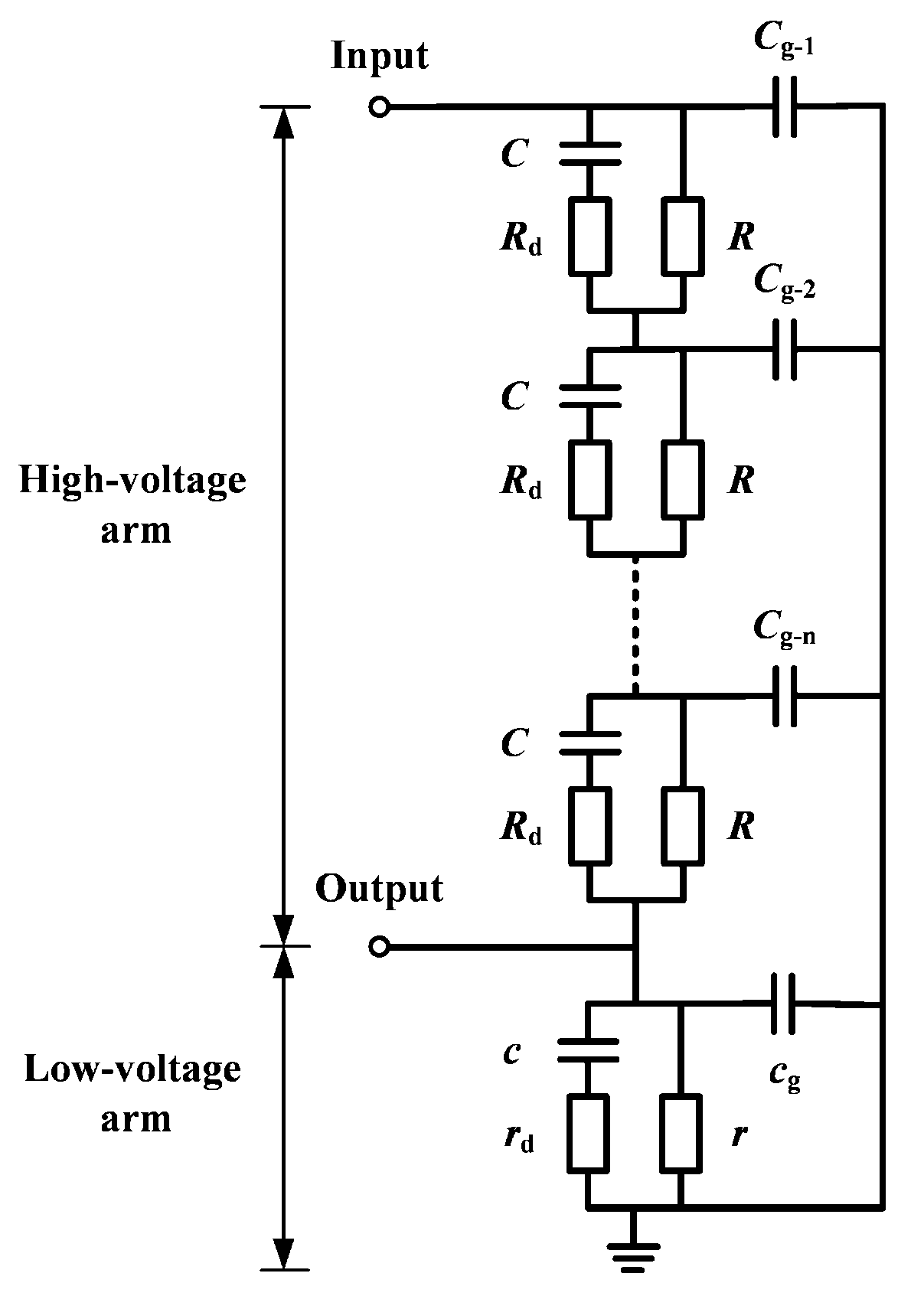
2. Structural Design
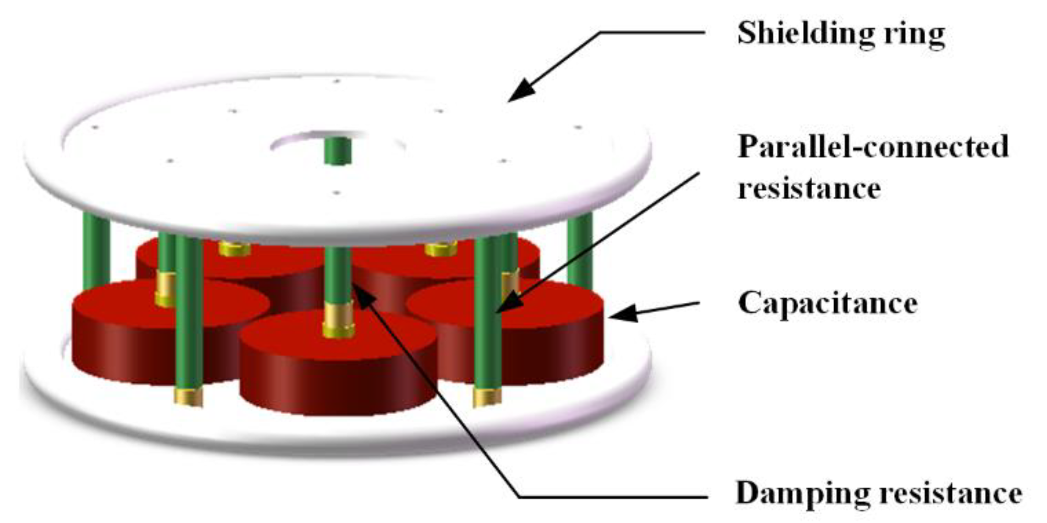
2.1. High-Voltage Arm
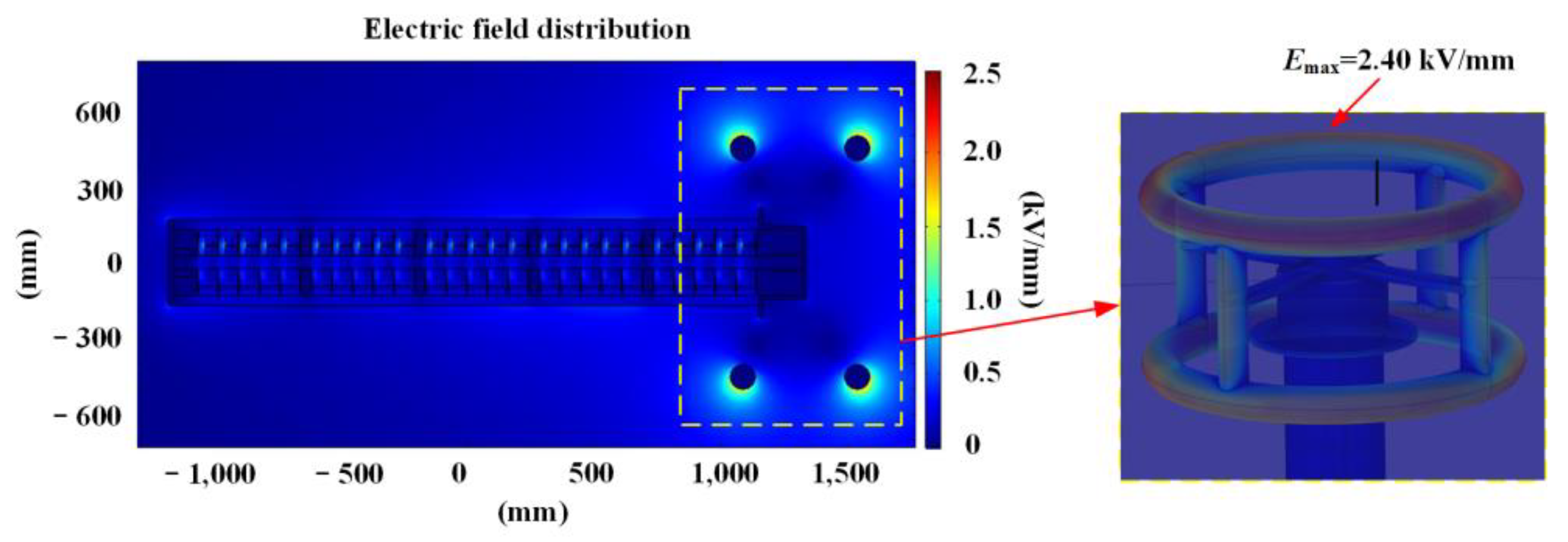
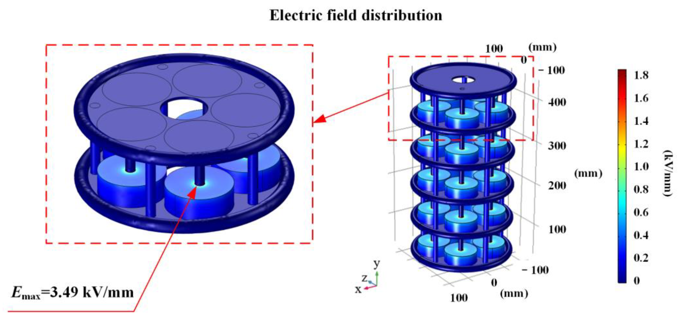
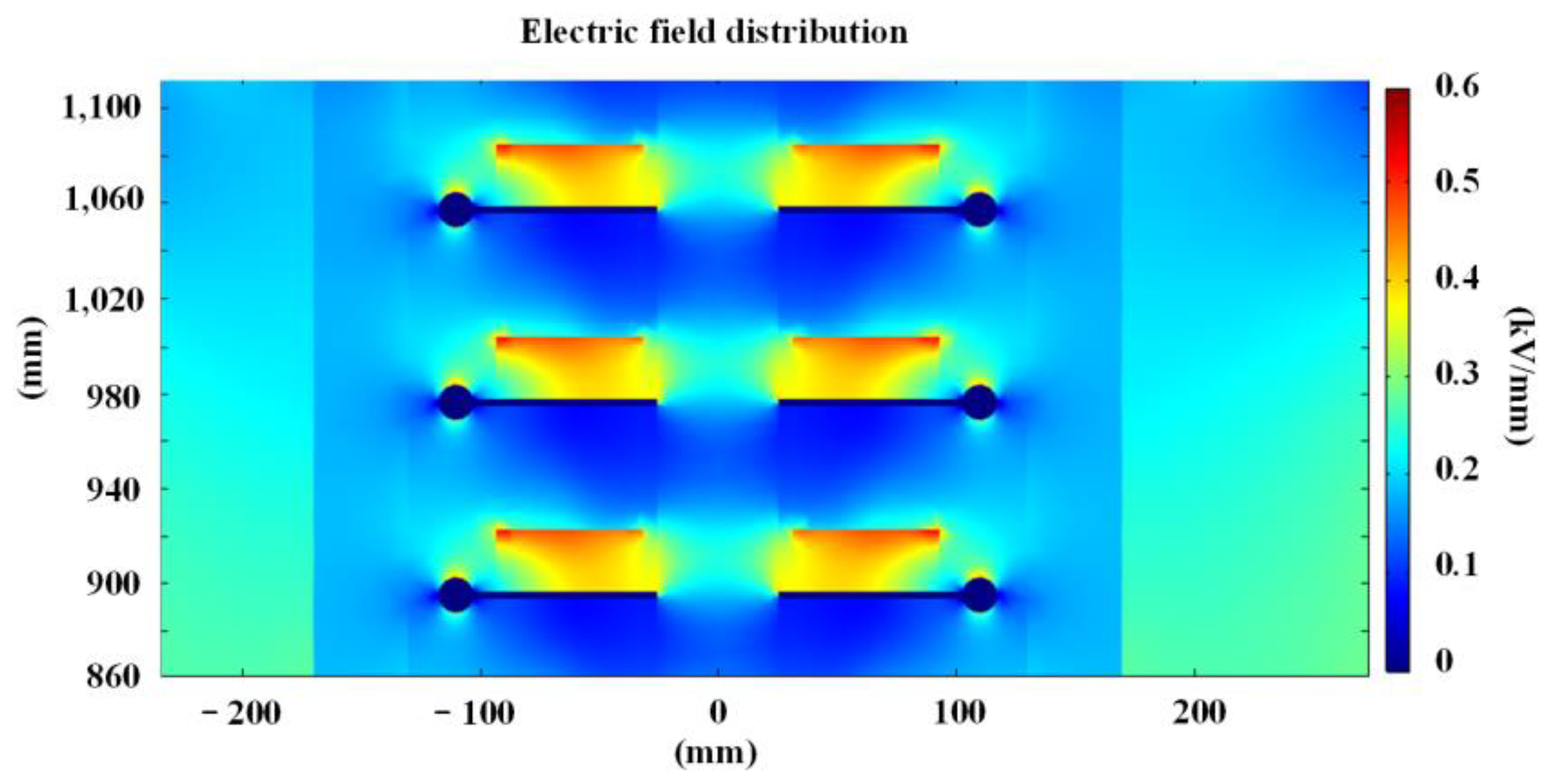
2.2. Field Distribution in the High-Voltage Arm
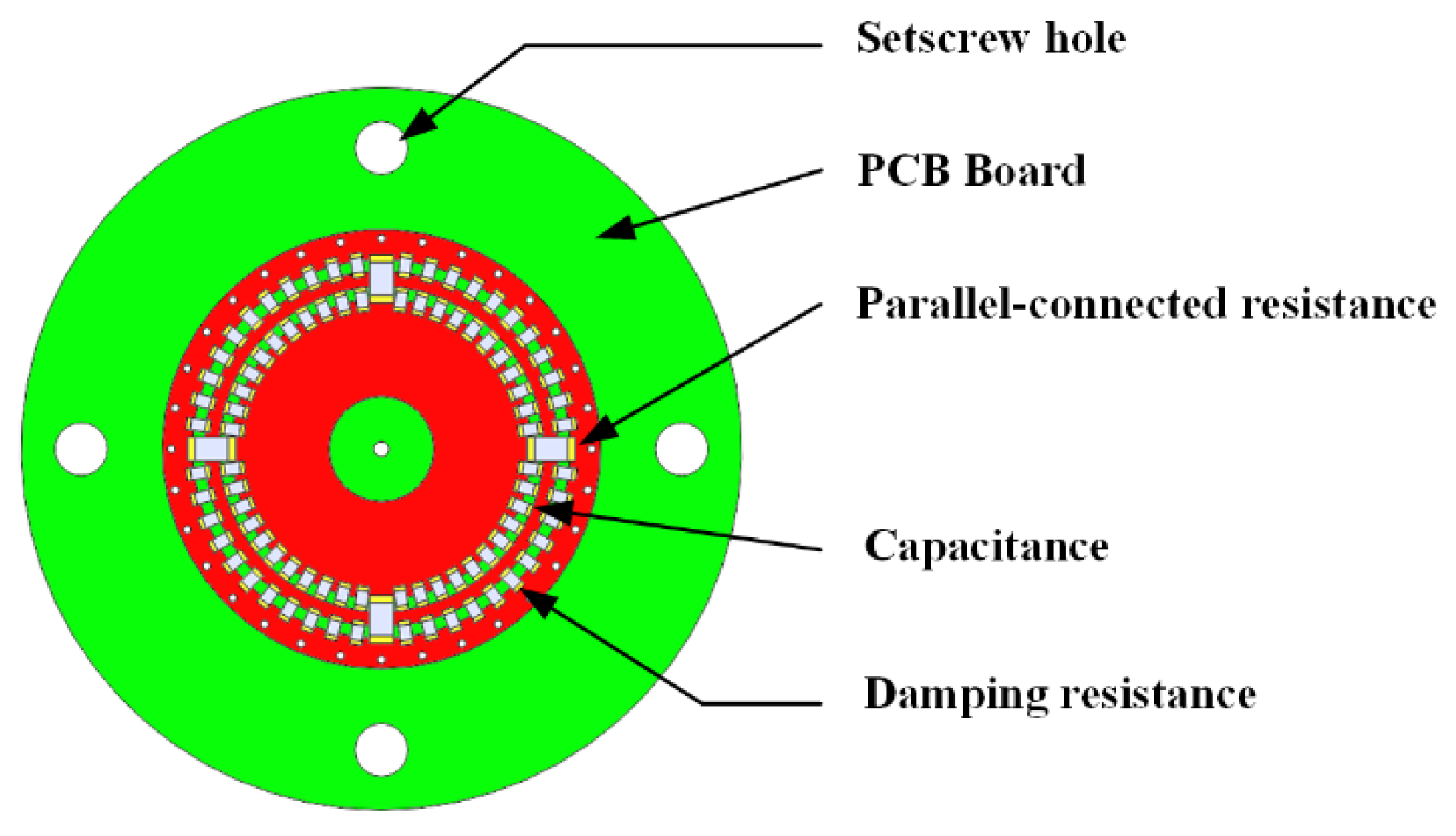
2.3. Low-Voltage Arm
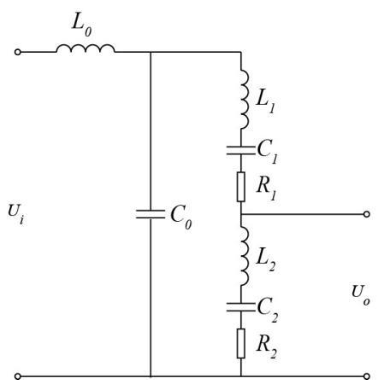
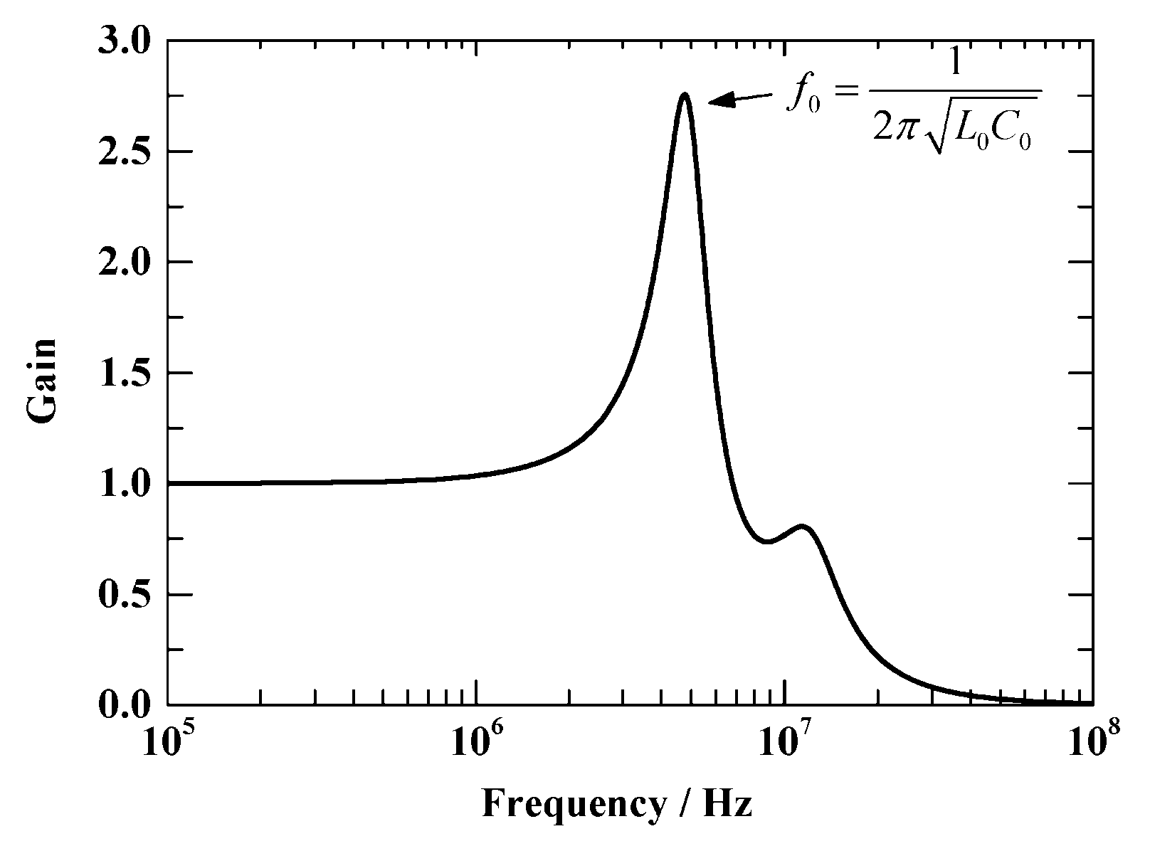
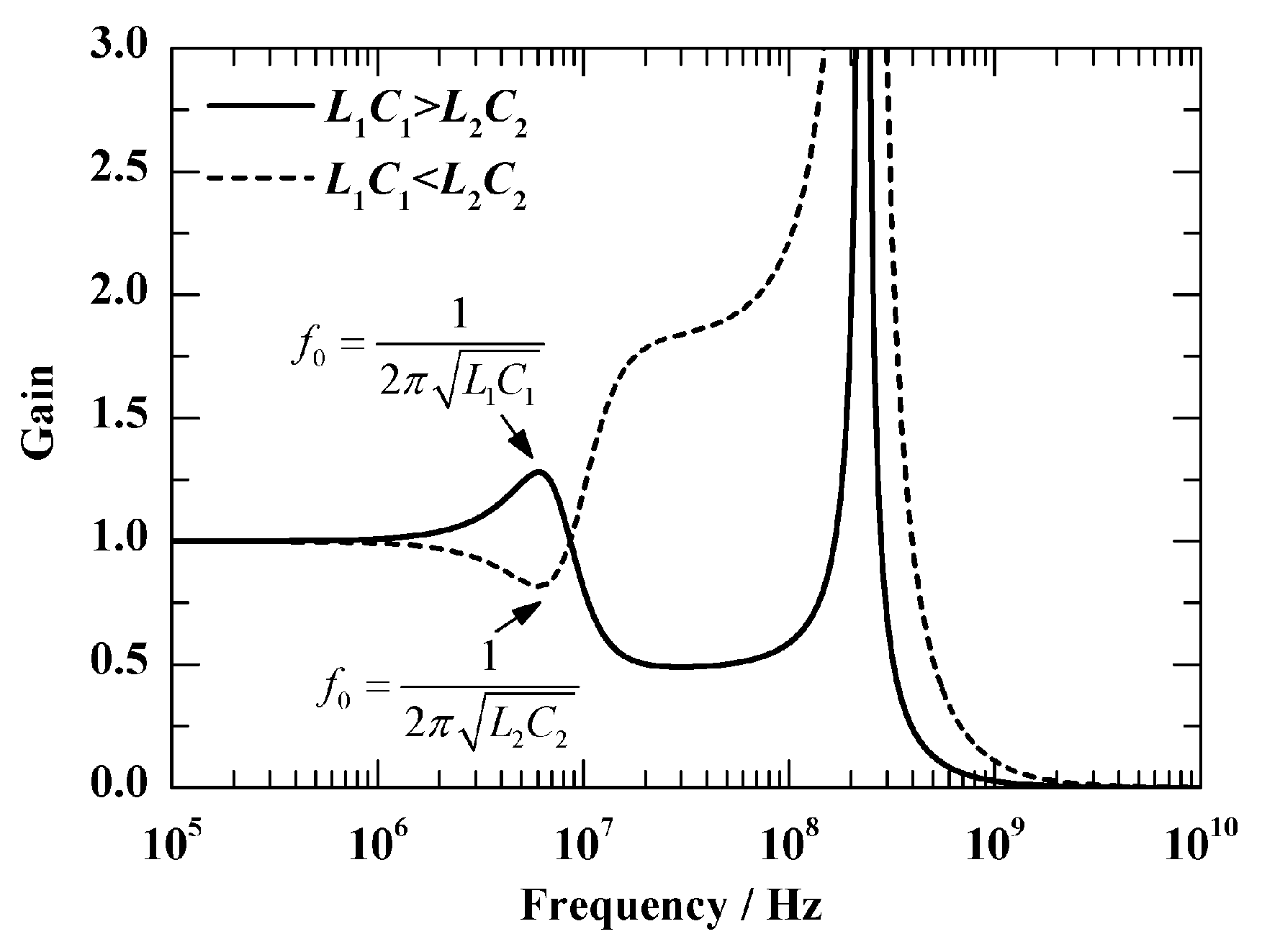
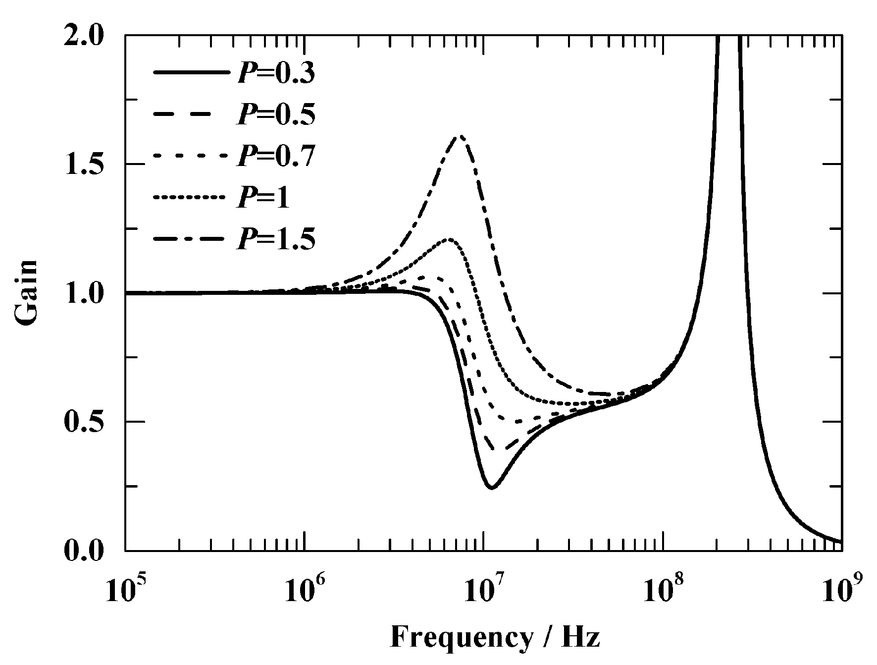
3. Frequency Response Analysis
4. Parameter Determination
4.1. High-Voltage Arm Components
4.2. Low-Voltage Arm Components
5. Performance Test
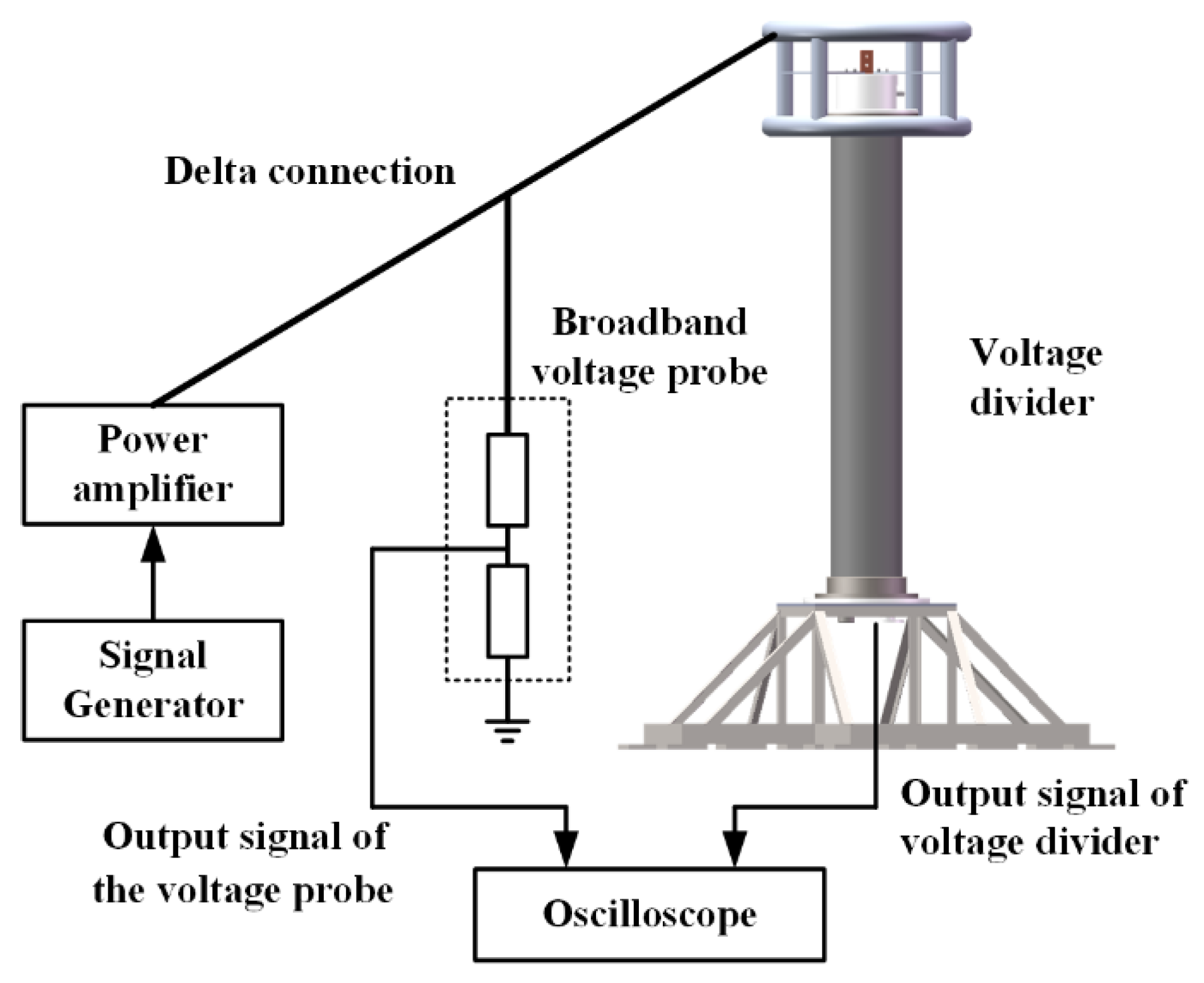
5.1. Test Rig
5.2. Calibration of Insulation Strength and Scale Factor
5.3. Temperature Stability
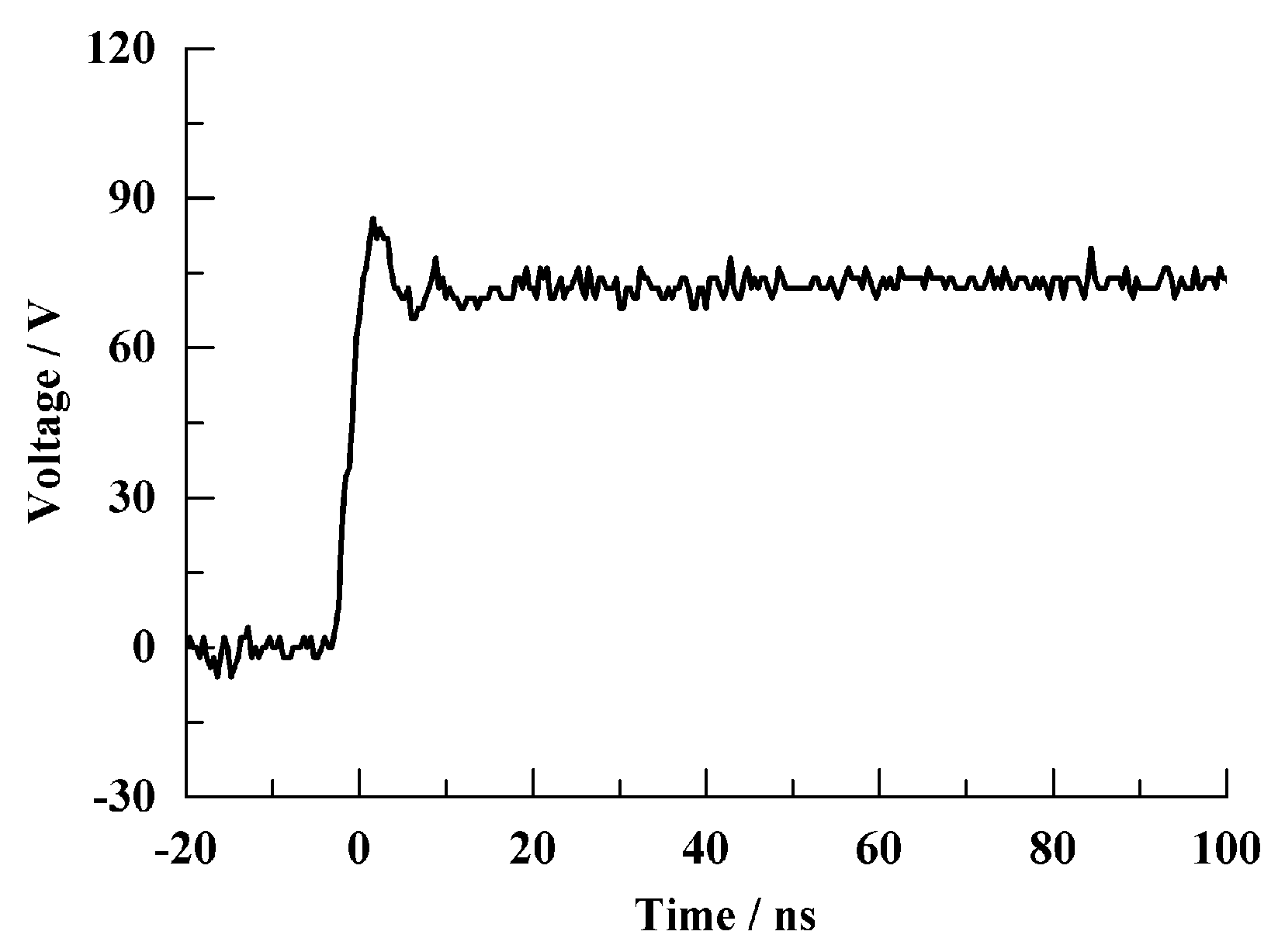
5.4. Step Response and Amplitude–Frequency Response
6. Conclusions
- (1)
- The internal electric field distribution of the voltage divider was optimized by using the structure of multi-stage series and multi-layer electrode plate shielding. The inductance of the high-voltage arm was reduced by adopting the circuit topology of multi-branch parallel connection, thus optimizing the response of the voltage divider.
- (2)
- The factors affecting the upper cut-off frequency were analyzed, and a method to increase the upper cut-off frequency was proposed based on the compensation resistor of the low-voltage arm.
- (3)
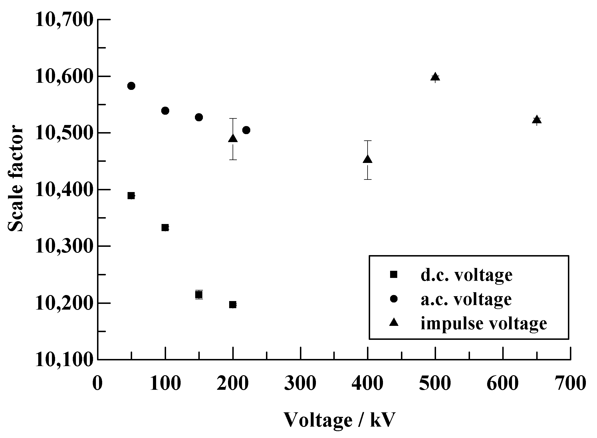
- The voltage divider meets the insulation requirements of high-voltage equipment, and the calibrated factor is 10,500:1. In the temperature range of −20~40 °C, the scale factor deviation is within 3% for measuring a DC voltage below 200 kV, a power frequency voltage below 220 kV and a lightning impulse below 700 kV.
- (4)
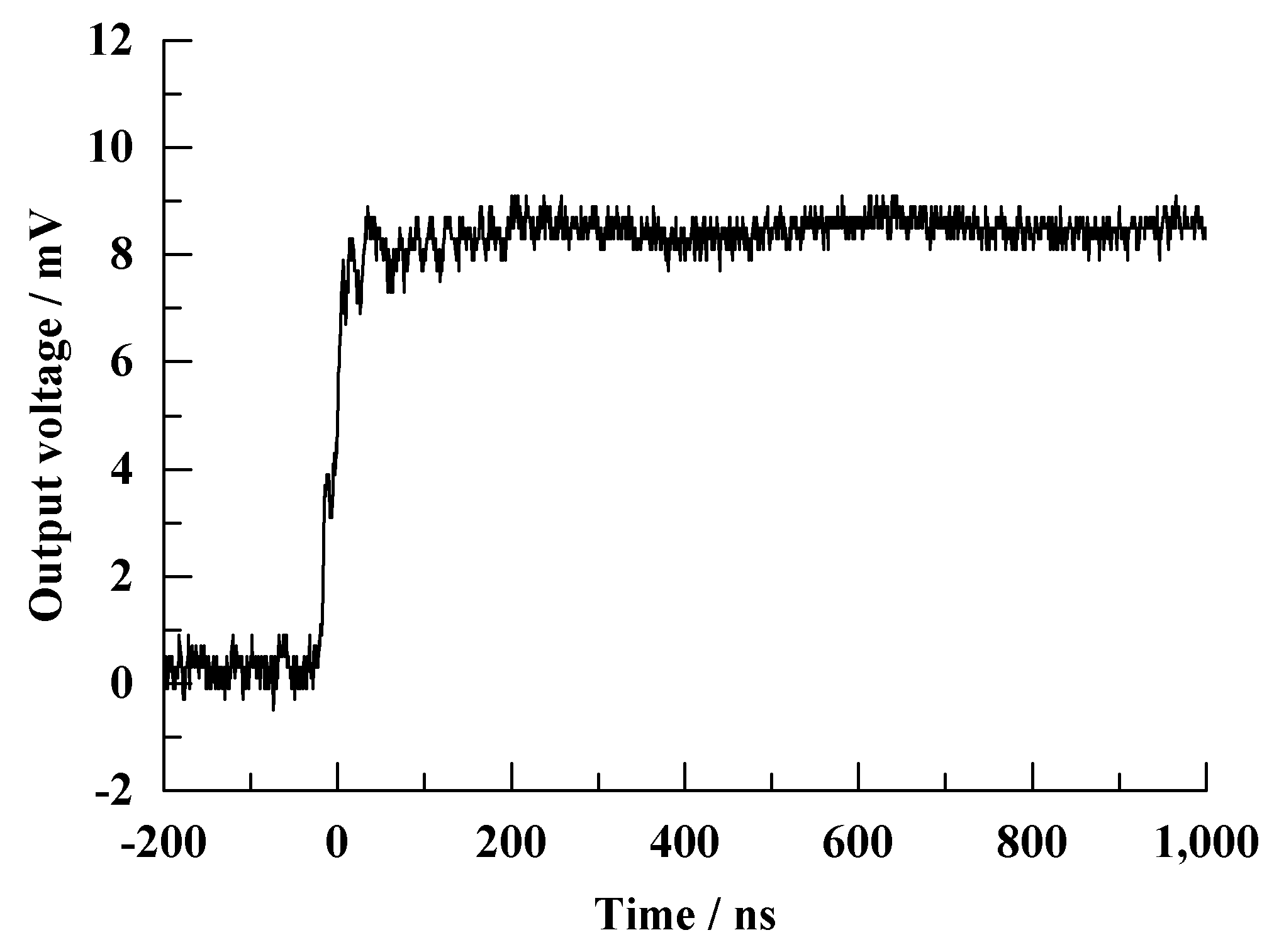
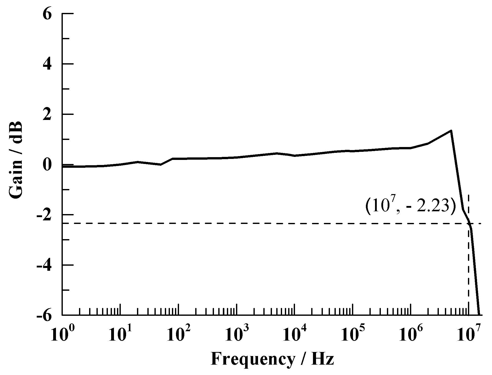
- For the step response, the rise time is about 29 ns, and the 3 dB bandwidth covers DC to 10 MHz.
Author Contributions
Funding
Conflicts of Interest
References
- Du, L.; Li, X.; Sima, W.X.; Xi, S.Y.; Yang, Q.; Yuan, T. Overvoltage On-line Monitoring System for 110 kV Substation and Its Waveform Analysis. High Volt. Eng. 2012, 38, 535–543. [Google Scholar]
- Zhou, X.; Qiu, Y.F.; Li, Z.J.; Miao, J. Transient Overvoltage On-line Monitoring Technology’s Today and Tomorrow. In Proceedings of the 2015 Annual Conference of CSEE, Wuhan, China, 17–20 November 2015. [Google Scholar]
- Zhang, C.Y.; Tang, S.; Liang, G.S.; Sun, H.F.; Wang, T.; Huang, T.; Ren, Y.Y. On-line Over-voltage Monitoring Method on Transmission Patameters of Voltage Transformer. In Proceedings of the 2011 Annual Conference of CSEE, Guiyang, China, 27–29 November 2011. [Google Scholar]
- Ming, Z.Q. Study on Overvoltage On-line Monitoring System of High-Voltage Network. Master’s Thesis, Chongqing University, Chongqing, China, 2008. [Google Scholar]
- Wang, Y.Q.; Xie, J.; Lv, F.C.; Li, M.; Yan, C.Y.; Bi, J.G.; Yuan, S. An Overvoltage Method Based on Composite Integral Rogowski Coil. Power Syst. Technol. 2015, 39, 1450–1455. [Google Scholar]
- Qiu, H.H. Investigations on the Key Technology and Relevant Theory of Electronic Transformers. Master’s Thesis, Dalian University of Technology, Dalian, China, 2008. [Google Scholar]
- Zhang, C.Y.; Li, W.B.; Chen, T. Online over-voltage monitoring algorithm based on broadband parameters of TV. High Volt. Eng. 2014, 40, 801–807. [Google Scholar] [CrossRef]
- Liu, B.; Ren, L.; Xu, X.H.; Yang, W.H.; Xu, Y. On-line over-voltage monitoring system based on virtual instrument. Electr. Power Autom. Equip. 2007, 27, 97–100. [Google Scholar]
- Pan, F.; Mu, Z.; Liu, H.; Wang, T.T.; Jiang, B.; Zhang, Y.; Zhang, C.M.; Xie, S.J.; Lin, G.S. Broadband Transient Model of CVT Based on Two-port Scaterring Parameters. Sichuan Electr. Power Technol. Volt. 2021, 44, 11–15. [Google Scholar] [CrossRef]
- Li, W. Research on Electronic Current Transformer and New Technology Applied in Digital Power Station. Master’s Thesis, Huazhong University of Science and Technology, Wuhan, China, 2011. [Google Scholar]
- Jiang, Y.H. Designation and Research on the Methods of Online Monitoring Divider of Overhead Transmission Line. Master’s Thesis, Xihua University, Chengdu, China, 2015. [Google Scholar]
- Kovacevic, U.D.; Stankovic, K.D.; Kartalovic, N.M.; Loncar, B.B. Design of capacitive voltage divider for measuring ultrafast voltages. Int. J. Electr. Power Energy Syst. 2018, 99, 426–433. [Google Scholar] [CrossRef]
- Brady, M.M.; Dedrick, K.G. High-Voltage Pulse Measurement with a Precision Capacitive Voltage Divider. Rev. Sci. Instrum. 1962, 22, 1421–1428. [Google Scholar] [CrossRef]
- Thomas, R.J. High-Impulse Current and Voltage Measurement. IEEE Trans. Instrum. Meas. 1970, 19, 102–117. [Google Scholar] [CrossRef]
- Hu, H.H. Study on Impulse Characteristics of Metallic Film Resistor and High-performance Resistive Divider. Master’s Thesis, Huazhong University of Science and Technology, Wuhan, China, 1989. [Google Scholar]
- Xie, S.J.; Zhang, C.M.; Ding, W.D.; Mei, K.S.; Han, X.Y.; Zhang, Y. Development and Uncertainty Evaluation of Sub-nanosecond Coaxial Resistive Divider. High Volt. Eng. 2020, 46, 4391–4399. [Google Scholar] [CrossRef]
- Liu, Y.; Lin, F.C.; Hu, G.; Zhang, M. Design and Performance of a Resistive-Divider System for Measuring Fast HV Impulse. IEEE Trans. Instrum. Meas. 2011, 60, 996–1002. [Google Scholar] [CrossRef]
- Harada, T.; Aoshima, Y.; Okamura, T.; Hiwa, K. Development of a high voltage universal divider. IEEE Trans. Power Appar. Syst. 1976, 95, 595–602. [Google Scholar] [CrossRef]
- Hällström, J.; Bergman, A.; Dedeoğ, L.S.; Elg, A.P.; Houtzager, E.; Klüss, J.; Lehtonen, T.; Lucas, W.; Meisner, J.; Merev, A.; et al. Performance of a Modular Wideband HVDC Reference Divider for Voltages up to 1000 kV. IEEE Trans. Instrum. Meas. 2015, 64, 1390–1397. [Google Scholar] [CrossRef]
- Zhou, K.; Zhang, T.; Dong, X.C.; Zhang, B.D.; Wang, J. Development of resistance-capacity divider for overvoltage online monitoring in distribution network. Electrotech. Appl. 2007, 26, 96–99. [Google Scholar]
- Tang, N.P.; Rou, S.Y.; Liao, F.W. Research on High-voltage Measurement Device based on Space Electric Field. Advaned Technol. Electr. Eng. Energy 2009, 29, 25–28. [Google Scholar] [CrossRef]
- Du, L.; Chang, A.F.; Sima, W.X.; Wang, Y.Y.; Lu, G.J. A non-contact overhead transmission line overvoltage sensor. Autom. Electr. Power Syst. 2010, 34, 93–97. [Google Scholar]
- Dong, C.F.; Xiong, Z.Z.; Xie, S.J.; Zheng, L.Q.; Wang, R.H.; Xiang, J. Research on Measuring Device for Wideband Transient Electric Field. Sichuan Electr. Power Technol. Volt. 2020, 43, 12–16. [Google Scholar] [CrossRef]
- Murase, H.; Okubo, H.; Aoyagi, H.; Yanabu, S. Development of 1-GHz GIS surge sensor. Electr. Eng. Jpn. 1989, 109, 32–38. [Google Scholar] [CrossRef]
- Hao, H. A NPO Capacitive Dialectical Material and Its Preparation Method: China. Patent 110171965 A, 27 August 2019. [Google Scholar]
- Ke, Y.G.; Cai, M.Y.; Zhao, H.Y.; Zhang, G.B.; Yang, W.; Tian, Y.; Zhu, T.Y. 3D Electric Field Simulation and Optimization of 40.5 kV Contact Box with Double Shield Structure. High Volt. Appar. 2020, 56, 23–28. [Google Scholar] [CrossRef]
- Wang, J.C.; Ding, W.D.; Qiu, A.C. Capacitive sensor for fast pulsed voltage monitor in transmission line. Rev. Sci. Instrum. 2019, 90, 035107. [Google Scholar] [CrossRef] [PubMed]
- Zhang, R.Y.; Chen, C.Y.; Wang, C.Z. High-Voltage Testing Technology; Tsinghua University Press: Beijing, China, 2009; ISBN 9787302204558. [Google Scholar]
- Xie, S.J.; Mu, Z.; Ding, W.D.; Wang, J.C.; Su, F.F.; Liu, Y. Development of the 100kV Square Wave Generator with Nanosecond Rise Time. High Volt. Eng. 2021, 47, 2169–2176. [Google Scholar] [CrossRef]
- Su, S.C.; Xie, S.J.; Ding, W.D.; Liu, Y.; Yan, J.Y.; Mu, Z. Development of 2 kV Square Wave Source with Sub-nanosecond Rise Time Using for the Calibration of VFTO Sensors. High Volt. Eng. 2020, 46, 2976–2983. [Google Scholar] [CrossRef]
- Yue, G.C.; Liu, W.D.; Chen, W.J.; Guan, Y.G.; Li, Z.B. Calibration of Very Fast Transient Overvoltage Measurement System for Ultra High Voltage Gas Insulated Switchgear. High Volt. Eng. 2012, 38, 342–349. [Google Scholar]
- Zeng, C. Relation between -3 dB frequency and risetime for resistive voltage divider. High Power Laser Part. Beans 2005, 17, 1065–1069. [Google Scholar]


| Material | Conductivity (S/m) | Relative Dielectric Constant |
|---|---|---|
| Parallel-connected resistor | 0.002 | 6 |
| Series-connected resistor | 788 | 6 |
| Capacitor | 1 × 10⁻¹² | 146 |
| Transformer oil | 1 × 10⁻¹² | 2.3 |
| Casing | 2.01 × 10⁻¹⁵ | 6 |
| Stainless-steel components | 4.03 × 10⁶ | 1 |
| Insulating pillar | 2.01 × 10⁻¹⁵ | 6 |
| Spherical solution domain | 5 × 10⁻¹⁴ | 1 |
| Standard Device Output/kV | Divider Output/V | Scale Factor |
|---|---|---|
| 49.929 | 4.8062 | 10,388 |
| 101.37 | 9.8091 | 10,335 |
| 152.42 | 14.921 | 10,215 |
| 203.53 | 19.964 | 10,195 |
| Standard Device Output/kV | Divider Output/V | Scale Factor |
|---|---|---|
| 49.721 | 4.6990 | 10,581 |
| 99.547 | 9.4464 | 10,538 |
| 148.78 | 14.132 | 10,528 |
| 218.34 | 20.789 | 10,503 |
| Standard Device Output | Divider Output | Scale Factor | ||||
|---|---|---|---|---|---|---|
| Peak/kV | Front Time/μs | Half-Width Time/μs | Peak/kV | Front Time/μs | Half-Width Time/μs | |
| 217.9 | 1.53 | 46.2 | 207.7 | 1.48 | 44.6 | 10,491 |
| 385.4 | 1.51 | 46.4 | 367.8 | 1.44 | 45.2 | 10,479 |
| 501.9 | 1.52 | 46.4 | 473.6 | 1.4 | 46.2 | 10,598 |
| 629.8 | 1.53 | 46.6 | 598.8 | 1.43 | 46.6 | 10,518 |
| Standard Device Output/kV | Divider Output/V | Scale Factor | |
|---|---|---|---|
| DC | 50.326 | 4.7889 | 10,509 |
| 100.95 | 9.6151 | 10,499 | |
| 150.86 | 14.521 | 10,389 | |
| 200.55 | 19.309 | 10,386 | |
| Power Frequency | 49.638 | 4.6214 | 10,741 |
| 99.620 | 9.2894 | 10,724 | |
| 148.83 | 13.863 | 10,736 | |
| 218.76 | 20.393 | 10,727 |
| Standard Device Output/kV | Divider Output/V | Scale Factor | |
|---|---|---|---|
| DC | 55.352 | 5.2021 | 10,640 |
| 107.29 | 10.081 | 10,643 | |
| 156.63 | 14.736 | 10,629 | |
| 204.85 | 19.454 | 10,530 | |
| Power Frequency | 49.883 | 4.6381 | 10,755 |
| 100.06 | 9.3180 | 10,738 | |
| 149.17 | 13.891 | 10,739 | |
| 219.59 | 20.457 | 10,734 |
Publisher’s Note: MDPI stays neutral with regard to jurisdictional claims in published maps and institutional affiliations. |
© 2022 by the authors. Licensee MDPI, Basel, Switzerland. This article is an open access article distributed under the terms and conditions of the Creative Commons Attribution (CC BY) license (https://creativecommons.org/licenses/by/4.0/).
Share and Cite
Xie, S.; Mu, Z.; Ding, W.; Wan, Z.; Su, S.; Zhang, C.; Zhang, Y.; Xia, Y.; Luo, D. Development of Broadband Resistive–Capacitive Parallel–Connection Voltage Divider for Transient Voltage Monitoring. Energies 2022, 15, 451. https://0-doi-org.brum.beds.ac.uk/10.3390/en15020451
Xie S, Mu Z, Ding W, Wan Z, Su S, Zhang C, Zhang Y, Xia Y, Luo D. Development of Broadband Resistive–Capacitive Parallel–Connection Voltage Divider for Transient Voltage Monitoring. Energies. 2022; 15(2):451. https://0-doi-org.brum.beds.ac.uk/10.3390/en15020451
Chicago/Turabian StyleXie, Shijun, Zhou Mu, Weidong Ding, Zhenbo Wan, Shaochun Su, Chenmeng Zhang, Yu Zhang, Yalong Xia, and Donghui Luo. 2022. "Development of Broadband Resistive–Capacitive Parallel–Connection Voltage Divider for Transient Voltage Monitoring" Energies 15, no. 2: 451. https://0-doi-org.brum.beds.ac.uk/10.3390/en15020451