
Design for a Four-Stage DC/DC High-Voltage Converter with High Precision and a Small Ripple
1
Aerospace Information Research Institute, Chinese Academy of Sciences, Beijing 100094, China
2
University of Chinese Academy of Sciences, Beijing 100049, China
*
Author to whom correspondence should be addressed.
Energies 2023, 16(1), 389; https://0-doi-org.brum.beds.ac.uk/10.3390/en16010389
Submission received: 6 December 2022
/
Revised: 23 December 2022
/
Accepted: 27 December 2022
/
Published: 29 December 2022
(This article belongs to the Special Issue Modeling, Control and Design of Power Electronics Converters)
Abstract
:This paper presents a four-stage DC/DC converter with high precision and a small ripple utilized in an electronic power conditioner (EPC). The galvanically isolated four-stage topology contains four cascade connections: a buck circuit, a push–pull circuit, a power converter, and a voltage regulator. The push–pull switches, as well as the diodes in the output-side rectifier, operate in zero-voltage switching (ZVS) and zero-current switching (ZCS) modes at both switch off and switch on, which helps increase the efficiency. The maximum efficiency of the converter can reach 94.5%. The buck circuit and voltage regulator operate in a two-stage closed-loop condition and, thus, the precision is greater than 0.02%. Due to the voltage regulator, the ripple is less than 1 V when the output voltage reaches 7000 V.
1. Introduction
Space traveling wave tubes amplifiers (STWTAs) [1], as the most important components of satellite systems, are mainly used to amplify the power of microwave signals [2]. An STWTA consists of a traveling wave tube (TWT) [3] and an electronic power conditioner (EPC) [4]. The TWT is a microwave vacuum electronic device [5]. The microwave signal can be amplified via energy exchange between electron injection and electromagnetic waves [6]. The main function of the EPC is to generate the high voltage required by the TWT via high-frequency and high-voltage power conversion technology [2,4,7].
The key performance indicators of the TWT, such as the phase shift, third-order intermodulation, and saturation gain, are directly affected by the voltage of the helix [1,8]. To ensure the working states and performance indicators of the STWTA, the high-voltage precision of the helix provided by the EPC should be greater than 0.05% [9]. Therefore, the high precision of high-voltage conversion becomes an important indicator of the EPC [10]. As the power supply of satellites come from solar energy conversion, whose efficiency is only approximately 28%, and the STWTA consumes 70% to 90% of DC energy, high efficiency also becomes a requirement of the EPC [2,5,11].
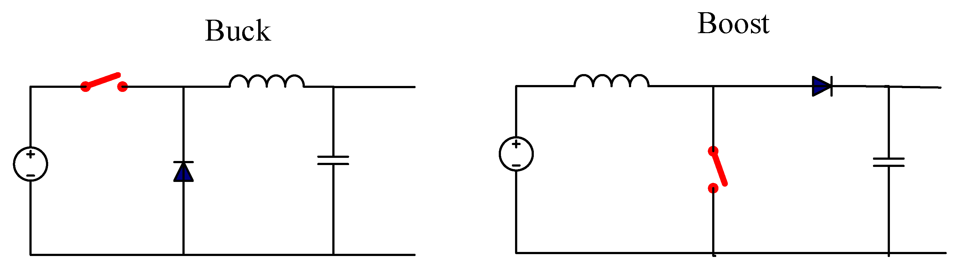
In recent years, EPC’s main research has focused on topology studies, which is categorized into single-stage power conversion and multi-stage power conversion [12,13]. The single-stage converters include buck, boost non-isolated topologies, and forward, flyback, push–pull, half-bridge, full-bridge, and other topologies. The multi-stage converter consists of two or more of these topologies. The topology described in [14] is a boost-based, non-isolated transformation topology. Compared with non-isolated topology, the advantages of an isolated topology are as follows: isolation protects the system from high voltages and currents caused by line surges or ground loops. The ground potentials in parts of a satellite are not equal, so ground currents are generated between systems. Without isolation, this current can introduce noise into the system, reduce measurement accuracy, and even destroy system components. The authors of [15] describe the difference between buck and boost topologies in many aspects. For example, to achieve the same ripple of inductor current, the boost topology needs more inductance than the buck, but the rms current through the inductor is much less than that of the buck, with the buck topology requiring a large and expensive capacitor to smooth the discontinuous input current. The buck and boost topologies are shown in Figure 1, and if a short-circuit fault occurs in the power switch (the red one) of the buck circuit, it does not affect the power supply; however, if the same fault happens in the boost circuit, the power supply will be short-circuited. In addition, the comparison of isolated topology characteristics is shown in Table 1.
To date, the major STWTA manufacturers in the world include the Tesat company in Germany [16,17,18], Thales company in France [19,20,21], and L-3 company [22,23] in the United States. The high-voltage precision of the EPC developed by L-3 is the best, reaching 0.03%. The ripple of the high voltage is approximately 1 V. The EPC developed by the Tesat company has a high efficiency that reaches 92.8%. Furthermore, in [24], an inductor-inductor-capacitor (LLC) resonant topology is proposed, with maximum efficiencies of 93.4% achieved at the output power of 5000 W, although the precision and the ripple of output voltage are not revealed. The authors of [25] describe the development of an 18 kV, 30 kW power supply for a pulsed current load whose output ripple is less than 0.01%, with the disadvantage of this design being the efficiency did not reach 90%.
Motivated by the above analysis, the high precision, small ripple of the output high voltage and the high conversion efficiency are difficult to be realized at the same time. Thus, an isolated four-stage DC/DC high-voltage converter is presented in this paper. This four-stage DC/DC converter topology enjoys the following advantages:
- The output high voltage can be controlled with a high accuracy of greater than 0.02%;
- The ripple of the output high voltage is less than 1 V at voltages reaching 7000 V;
- The efficiency of the converter can reach up to 94.5%.
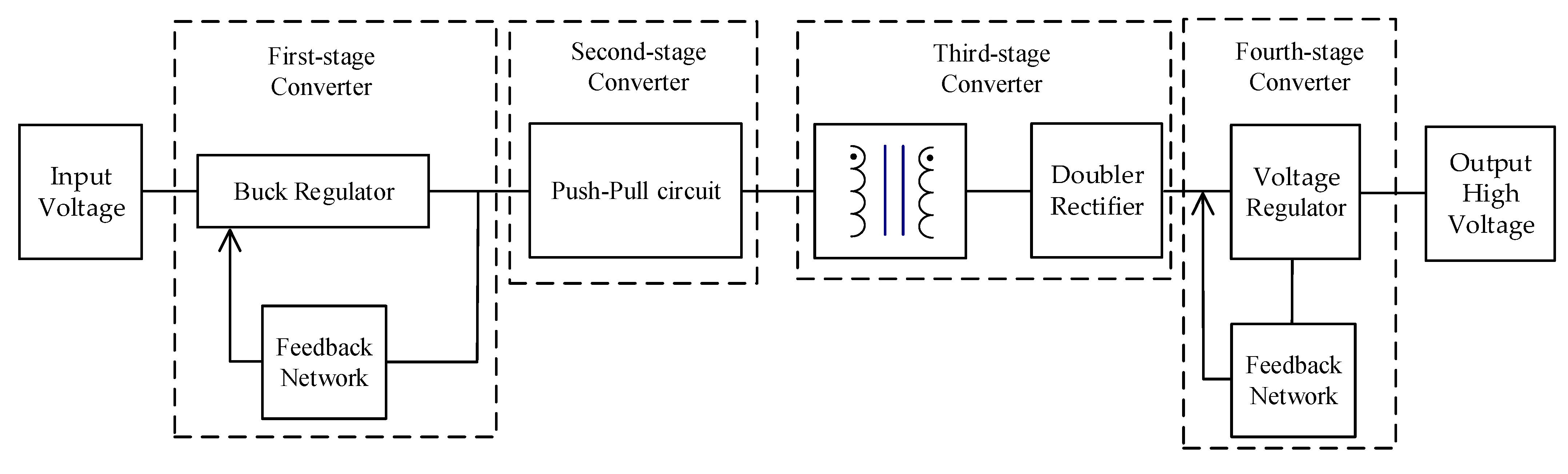
The block diagram of this topology is shown in Figure 2.
As shown in Figure 2, the four-stage DC/DC high-voltage converter consists of a buck circuit, a push–pull circuit, a power converter, and a voltage regulator. The bus voltage in the satellite is transformed into a high voltage for the TWT through this four-stage converter.
The content of this paper starts with Section 2, which introduces the principle and the calculation of key parameters. Section 3 presents the experimental results of laboratory prototype. Section 4 describes the advantages and disadvantages of this topology, and the areas for improvement. Finally, conclusions are drawn in Section 5.
2. Principle Introduction and Calculation of Key Parameters
2.1. Principle Introduction
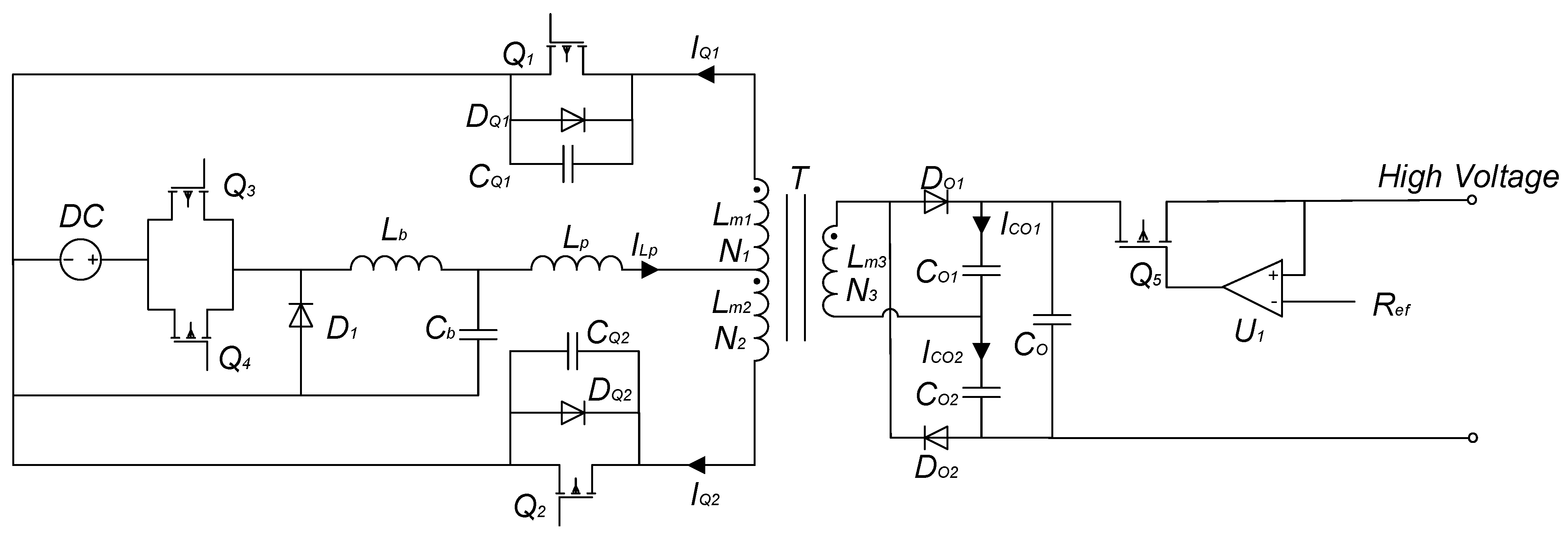
A four-stage DC/DC high-voltage converter is proposed in this paper, with the topology of the schematic circuit depicted in Figure 3.
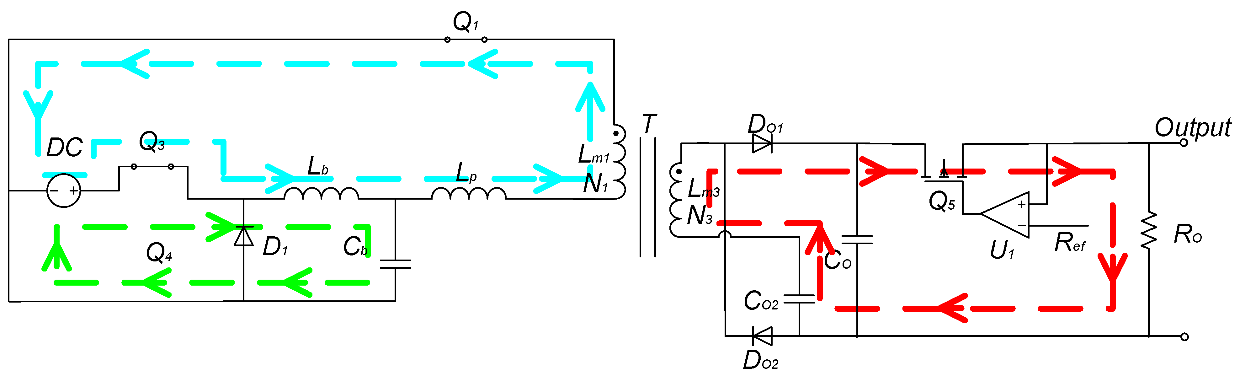
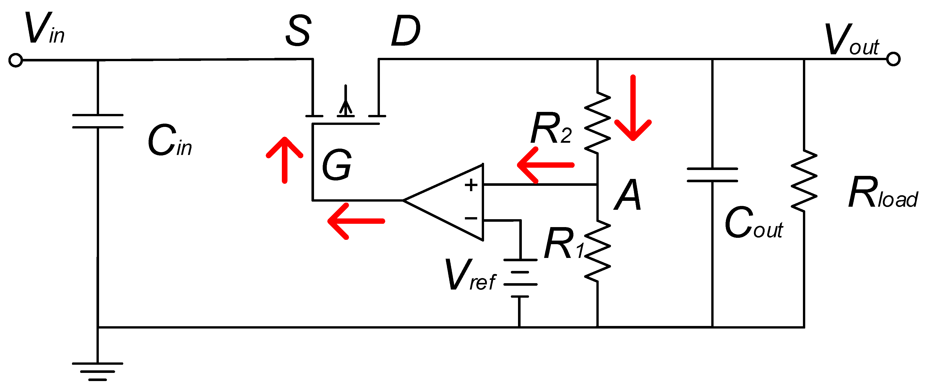
In Figure 3, , , , , and form the first stage of transformation, an interleaved dual-driver buck circuit, where and are interleaved switches, is the fly-wheel diode, and and are the inductance and capacitance, respectively, of the buck circuit. The switches and form the second stage of transformation: a push–pull circuit, where and are the body diodes of and , respectively, and and are the parasitic output capacitance. The power transformer T and the doubler rectifier circuit form the third stage of conversion, where is the equivalent primary leakage inductance, , , and are the voltage-doubling rectifier diodes and capacitances, and is the filter capacitor. Switch and high-precision operational amplifier U1 form the fourth stage of transformation, i.e., a low-dropout regulator (LDO).
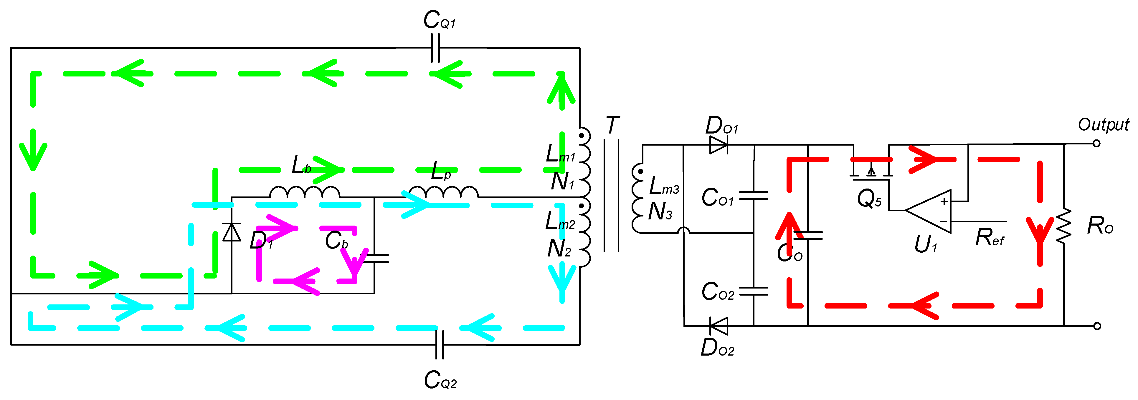
When and are both turned off, the equivalent circuit diagram is shown in Figure 4. On the primary side, part of the energy in charges the capacitor , while the other part flows through , , , , and sequentially, and then returns to . On the secondary side, the current flows through , , , and to form a loop. There is no energy exchange between the primary side and the secondary side. In Figure 4, the green, blue, and purple arrows indicate the direction of current flow on the primary side, the red arrows indicate the direction of current flow on the secondary side.
Since there is no energy exchange between the primary side and the secondary side, the voltage across can be considered constant, with the equivalent circuit of Figure 4 depicted in Figure 5.
Therefore:
As and , then, neglecting the effect of the leakage inductance, it is , so that yields:
Combining (1) and (2):
The solution of (3) is:
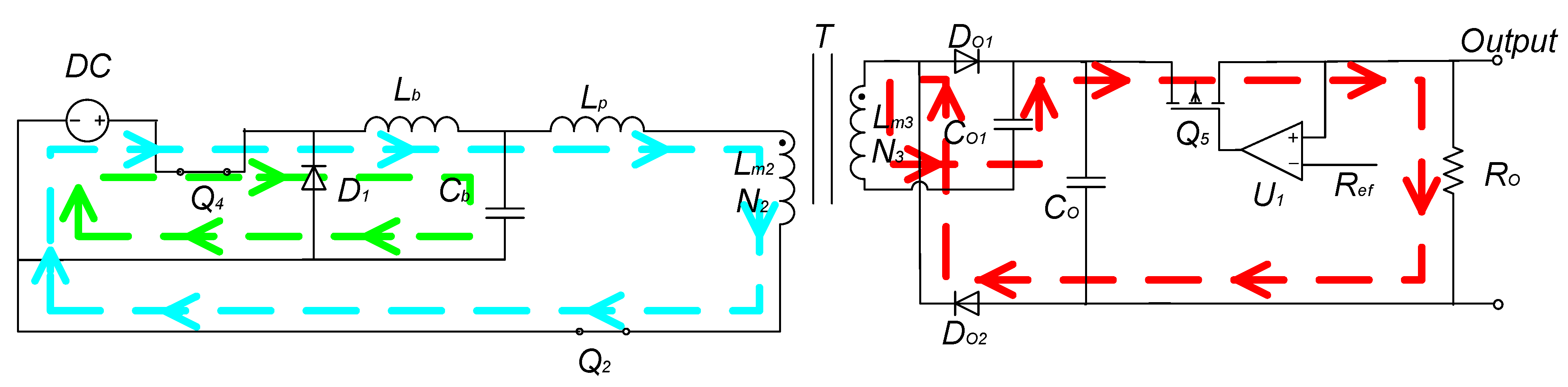
When is turned on, energy transfers from the primary side to the secondary side, with the equivalent circuit diagram shown in Figure 6. In Figure 6, the green and blue arrows indicate the direction of current flow on the primary side, the red arrows indicate the direction of current flow on the secondary side.
According to KCL,
Hence,
whose solution is:
The equivalent circuit diagram when is turned on is depicted in Figure 7. In Figure 7, the green and blue arrows indicate the direction of current flow on the primary side, the red arrows indicate the direction of current flow on the secondary side.
When the transformation enters the steady state, the ratio of input and output voltage is:
where
- D is the duty cycle of interleaved switches;
- is the number of turns on the secondary side of the transformer;
- is the number of turns on the primary side of the transformer;
- is the pressure drop setting value of the MOSFET in the LDO module.
In the high-voltage conversion process, the loss of the switch tubes accounts for a large part. To achieve high efficiency, the switch tubes of the second-stage converter (push–pull circuit), which are connected to the third-stage converter (main power converter), should implement a soft switching process, namely, zero-voltage switching (ZVS) and zero-current switching (ZCS), at both switch off and switch on, and the rectifier diode in the voltage-doubling rectifier circuit should achieve ZCS to reduce the loss in the switching process.
In this design, the buck circuit and push–pull circuit use the components themselves to generate resonances to achieve soft switching without the need for additional resonant components. The capacitance in the buck circuit and the leakage inductance of the main power transformer are fully utilized to form a resonant cavity.
After the first three levels of transformation, the output voltage is actually a high DC voltage with an AC component, and the peak value of the AC component is approximately 10 V. The existence of this AC component will seriously affect the phase shift, third-order intermodulation, saturation gain, and other performance indicators of the TWT, so this high voltage cannot be directly used to power the TWT. The LDO module is used to reduce the AC component so that the high voltage becomes a purer DC voltage. The principle of the fourth-stage converter LDO is shown in Figure 8. In Figure 8, red arrows indicate feedback paths of LDO.
When drops due to load changes or other reasons, the voltage across the series divider resistor will also drop, and then the voltage at point A drops. The voltage at point A is compared with , and the error amplifier will reduce the output so that the voltage at G decreases, the voltage does not change, and the voltage difference then increases. The output current increases, and this increase will make rise, completing feedback control so that returns to the normal voltage. By selecting and screening high-precision resistors to precisely control the divider ratio of two series resistors and , the output voltage can be accurately controlled. In this design, the is fixed, but if it changes, the divider ratio of and can be adjusted to change the noninverting input of the operational amplifier to keep the output of the operational amplifier constant, while the MOS tube operates in the linear region to ensure that the output voltage does not change.
2.2. Calculation of Key Parameters
According to the actual conditions in EPC applications, the input voltage , the output voltage , the load power , and the switching frequency . The calculation of key parameters is as follows.
A resonant cavity is formed between and , and the resonant frequency is the switching frequency.
Depending on how the transformer is wound, may differ, and adjusting can achieve the switching frequency requirements. The lamination winding method is adopted for the main power transformer in this case, and the test result of the leakage inductance is 0.6 μH.
Therefore, the buck capacitance can be calculated as:
The inductance of the buck circuit can be calculated as:
where is the output voltage of the buck circuit, with ;
is the duty cycle of interleaved switches;
is the ripple current rate, with generally; and is the root mean square (RMS) current of the buck output,
The number of turns on the primary side of the transformer can be calculated as:
where
- is the waveform factor of the square wave, with ;
- is the switching frequency, with ;
- is the magnetic flux density, in which the TPW33-UYF36 series is adopted as the type of magnetic core, with ;
- and is the effective cross-sectional areas of the core, with .
Therefore, and an integer value is taken, that is, .
The number of turns on the secondary side of the transformer is:
Taking an integer value, .
3. Experimental Validation
According to the above principle and the parameter calculation, a prototype of a four-stage converter is fabricated. The input voltage , the output voltage , the load power , and the switching frequency .
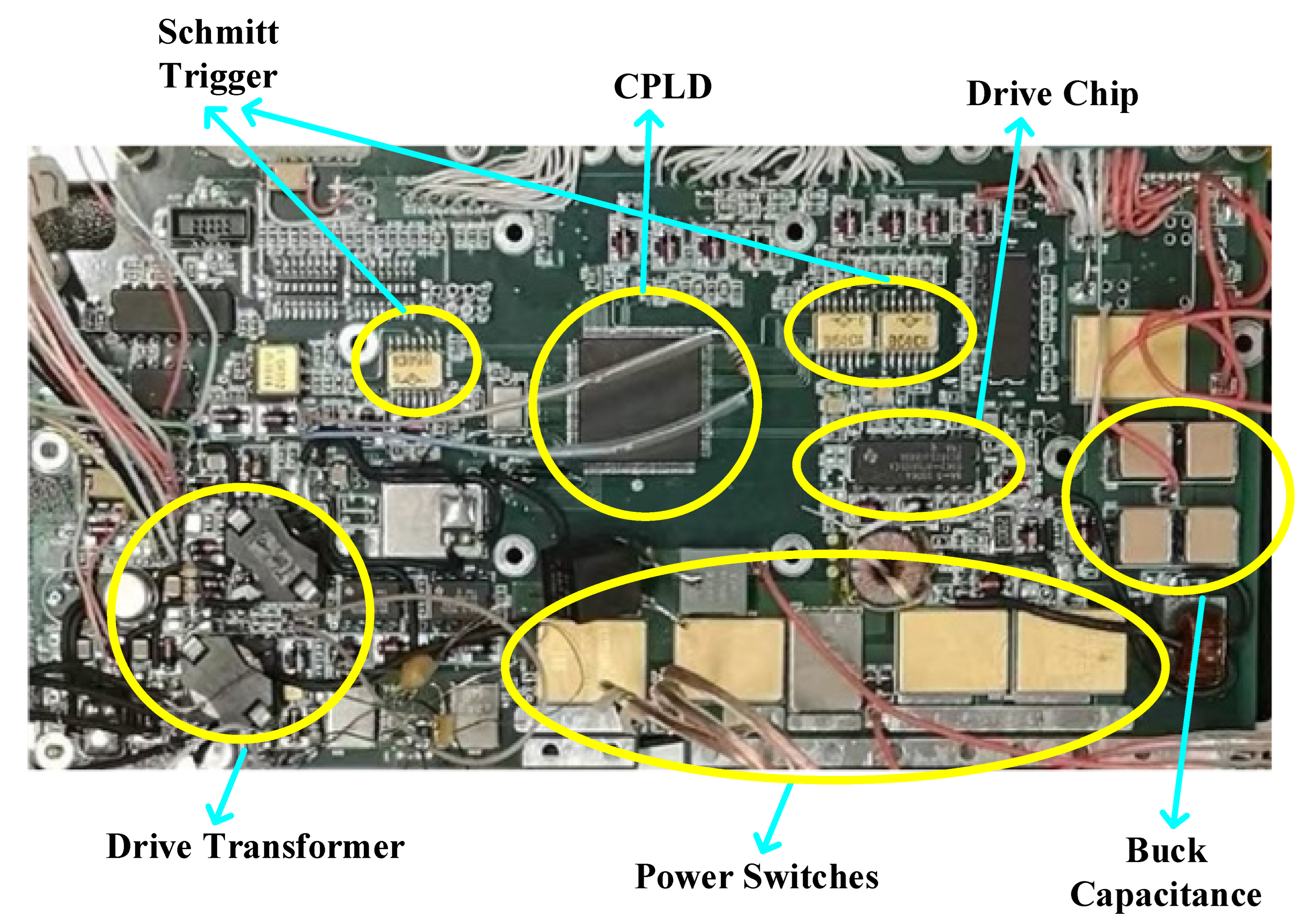
A laboratory prototype of the four-stage converter was fabricated, as shown in Figure 9. There are four power switches in the converter, with two switches used as interleaved dual-driver in the buck circuit and the other two switches used in the push–pull circuit. The main uses of Schmitt triggers are waveform shaping, transformation, comparison, etc. All of the control signals are processed in CPLD.
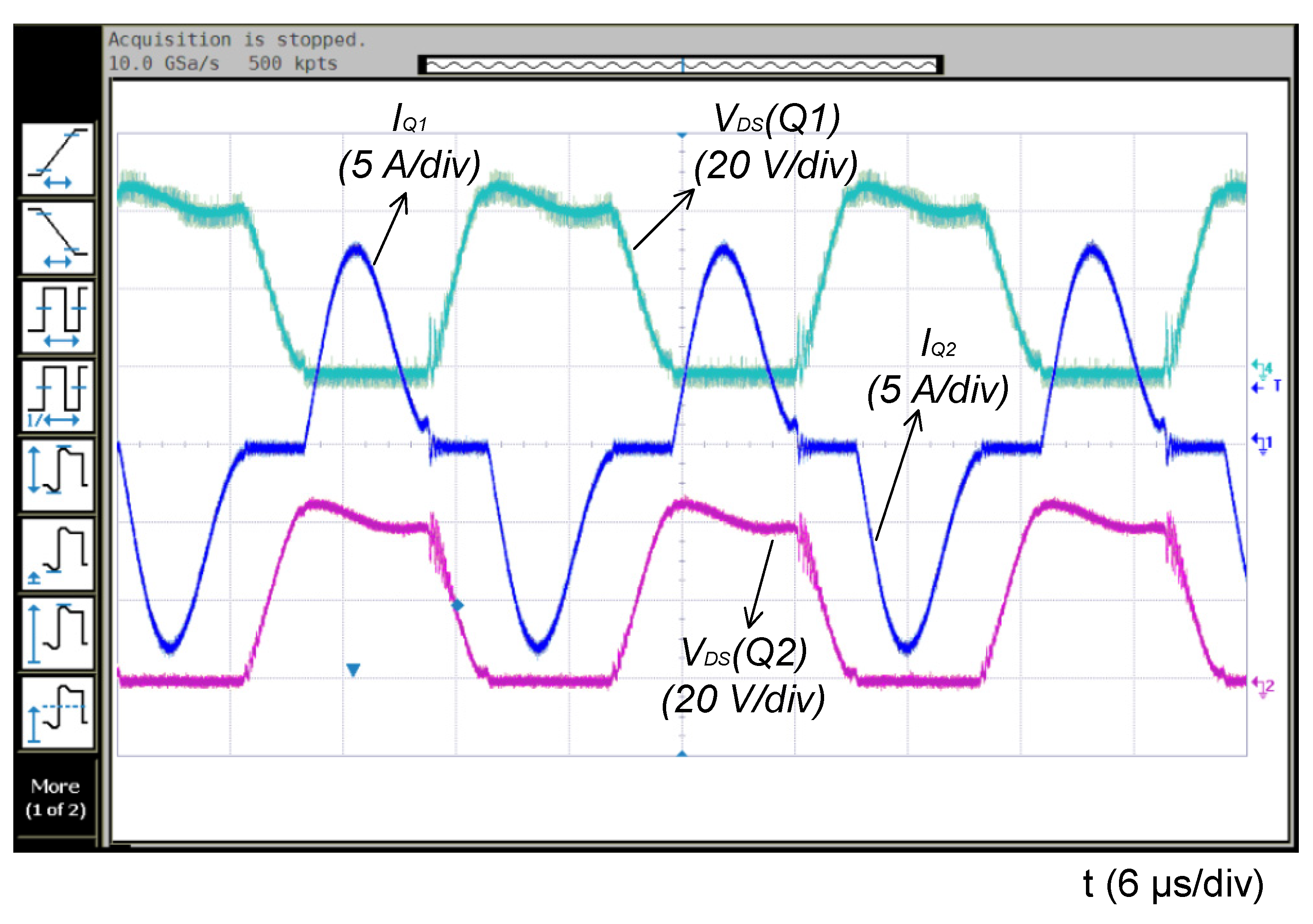
The voltage and current waveforms of the second-stage push–pull switches of the prototype are presented in Figure 10.
Figure 10 shows that the voltage waveform at the DS terminal of the push–pull switches and is approximately a trapezoidal wave, and the current waveform flowing through the switches is close to a sine wave, without obvious voltage spikes or current overshoots. ZCS and ZVS can be realized at both turning on and off. The voltage stress of the switches in the push–pull circuit is:
The peak current of the switches is:
where is the operating frequency of dual interleaved drivers, is the off time of the switches, and is the on time of the switches.
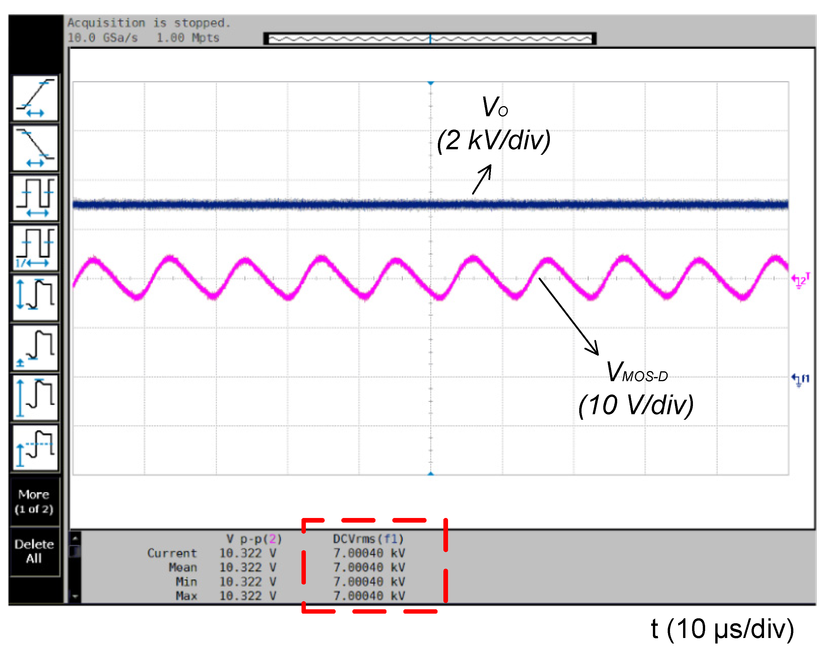
After the first three stages of conversion, the voltage flows into the fourth-stage converter LDO, as shown in Figure 11 (), and the ripple is approximately 10 V. With a 1000:1 high-voltage probe of oscilloscope (which the maximum measurement voltage can reach 15 kV), the test value of the output high voltage after passing through the LDO module obtained by an oscilloscope is also shown in Figure 11 (). According to the test result of (inside the red dashed box), the output high voltage is 7000.4 V DC.
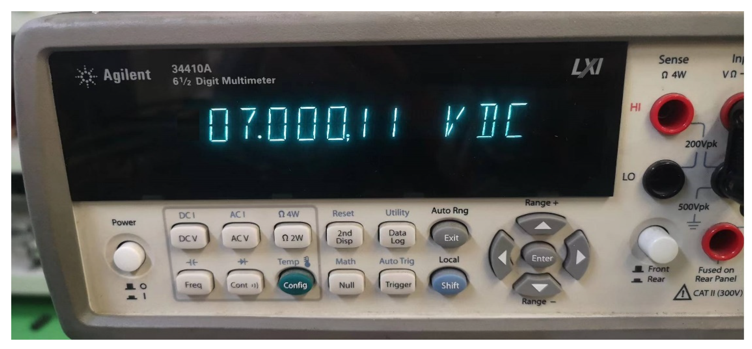
The test value of the output high voltage obtained by a digital multimeter is shown in Figure 12. The digital multimeter performs measurements with a 1000:1 probe, so the test value is 7.00011 V DC.
The test values of both the oscilloscope and digital multimeter are 7000 V, indicating that the output voltage accuracy of this four-stage DC/DC converter is greater than 0.02%.
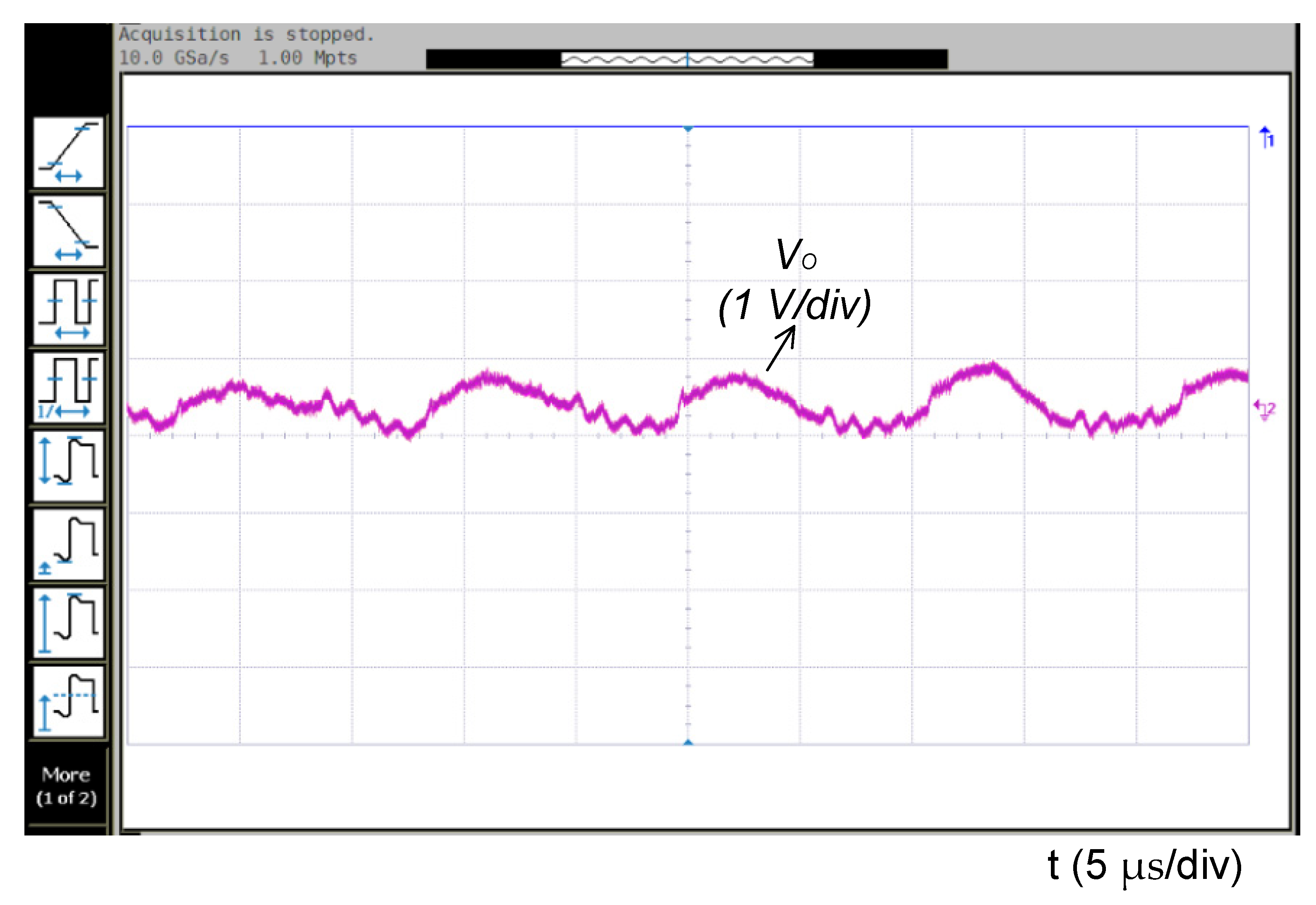
When the output high voltage is 7000 V, the high-voltage ripple is approximately 0.8 V, as shown in Figure 13, indicating that the voltage ripple is greatly reduced after the fourth-stage LDO conversion, with the ripple less than 1 V.
Since the LDO module, the output high voltage does not change while the input voltage differs, with the efficiency calculated as follows:
where and can be read from the DC input power supply and is measured by stringing into a multimeter.
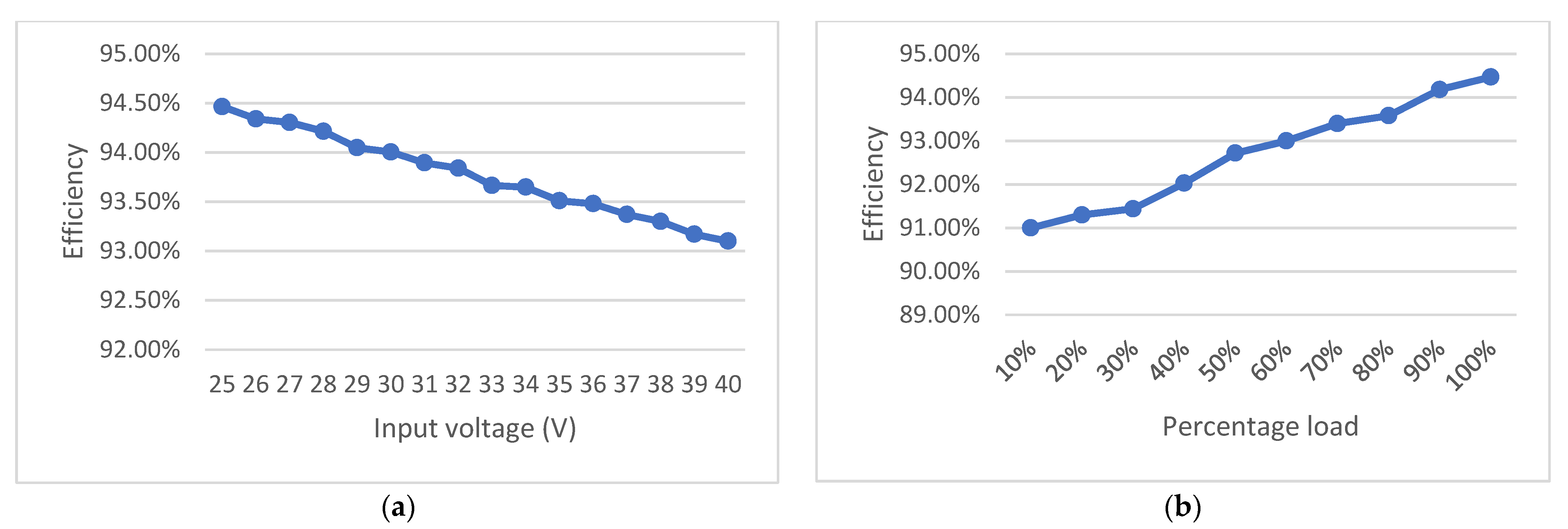
Figure 14 shows the efficiency test of this four-stage converter. In Figure 14a, with a full load, the efficiency is tested at different bus input voltages, which indicates that the lower the bus input voltage is, the higher the potential efficiency. The bus voltage on a satellite is usually 25~40 V DC, and the efficiency of this four-stage converter can reach 94.5%. In addition, Figure 14b shows the efficiency results for different loads when the input voltage is 25 V, with the graph suggesting that the heavier the load, the higher the efficiency.
4. Discussion
The four-stage DC/DC high-voltage converter is composed of a buck circuit, a push–pull circuit, a power converter, and an LDO regulator, with the first three stages of conversion being typical switching power conversion, which is characterized by high efficiency. However, the working principle of the LDO is to apply an excess voltage that is higher than the set value to the switch to form a DS voltage drop and to simultaneously make the switch work in the linear region to achieve the voltage regulation function; thus, the loss of the switch will increase and the efficiency will be relatively low. In subsequent work, an approach for improving the conversion efficiency of the LDO will be studied to further improve the efficiency of the EPC. Additionally, the switches of the first-stage converter operate in hard-switching mode, and a method for higher efficiency of the buck circuit will be researched.
5. Conclusions
This paper investigated the research status of EPC and showed that it is difficult to meet high accuracy, small ripple, and high efficiency at the same time. Therefore, in order to achieve high accuracy, small ripple, and high efficiency, a four-stage DC/DC high-voltage converter topology is proposed in this paper, with the advantages of the converter verified through the experimental results of a prototype, which proves that this converter topology has the following characteristics:
- The output high voltage can be controlled with a high accuracy of greater than 0.02%;
- The ripple of the output high voltage is small, less than 1 V at voltages up to 7000 V;
- The power switches in the push–pull circuit can realize ZVS and ZCS at both turning on and off, with the efficiency of the converter reaching 94.5%.
Author Contributions
Conceptualization, W.Z., X.S. and G.W.; methodology, W.Z., X.S., G.W. and B.Z.; software, W.Z. and X.H.; validation, W.Z. and C.H.; formal analysis, W.Z.; investigation, W.Z.; resources, W.Z. and C.H.; data curation, W.Z. and C.H.; writing—original draft preparation, W.Z.; writing—review and editing, B.Z., X.S., G.W. and X.H.; visualization, C.H.; supervision, W.Z.; project administration, W.Z.; funding acquisition, W.Z. All authors have read and agreed to the published version of the manuscript.
Funding
This paper is a part of the project named Application of High Efficiency Partial Power Regulation on Space Travelling-wave Tube Amplifiers (No. 62201546), which is sponsored by National Natural Science Foundation of China.
Data Availability Statement
Not applicable.
Conflicts of Interest
The authors declare no conflict of interest.
References
- Wang, X.-N.; Su, X.-B.; Ma, D.-D.; Zhang, R.; Miao, G.-X.; Wang, W.-L. In-Orbit Reliability Evaluation of Space TWTA Based on Copula Function and Bivariate Hybrid Stochastic Processes. Appl. Sci. 2022, 12, 1575. [Google Scholar] [CrossRef]
- Zheng, W.; Hu, C.; Zhao, B.; Su, X.-B.; Wang, G.; Hou, X.-W.; Gu, B. A Two-Stage DC/DC Isolated High-Voltage Converter with Zero-Voltage Switching and Zero-Current Switching Applied in Electronic Power Conditioners. Energies 2022, 15, 6378. [Google Scholar] [CrossRef]
- Wang, Y.; Dong, Y.; Zhu, X.; Guo, J.; Xu, D.; Wang, S.; Gong, Y. Multiple Dielectric-Supported Ridge-Loaded Rhombus-Shaped Wideband Meander-Line Slow-Wave Structure for a V-Band TWT. Electronics 2022, 11, 405. [Google Scholar] [CrossRef]
- Zhao, B.; Wang, G.; Hurley, W.-G. Analysis and Performance of LCLC Resonant Converters for High-Voltage High-Frequency Applications. IEEE J. Emerg. Sel. Top. Power Electron. 2017, 5, 1272–1286. [Google Scholar] [CrossRef]
- Zhao, B.; Wang, G. PSO-Algorithm-Based Optimal Design of LCLC Resonant Converters for Space Travelling-Wave Tube Amplifiers Applications. Energies 2019, 12, 2444. [Google Scholar] [CrossRef] [Green Version]
- Abdulla, M.; Juhany, K.A. A Rapid Solver for the Prediction of Flow-Field of High-Speed Vehicle Moving in a Tube. Energies 2022, 15, 6074. [Google Scholar] [CrossRef]
- Weinberg, A.H.; Ghislanzoni, L. A New Zero Voltage and Zero Current Power-Switching Technique. IEEE Trans. Power Electron. 1992, 7, 655–665. [Google Scholar] [CrossRef]
- Zhou, S.; Yao, Y.; Zhang, Y. Electromagnetic Particle Algorithm for Beam–Wave Interaction in Traveling Wave Tube of Symmetry. Symmetry 2022, 14, 2119. [Google Scholar] [CrossRef]
- Kowstubha, P.; Krishnaveni, K.; Ramesh, R.K. Electronic Power Conditioner for Ku-Band Travelling Wave Tube. J. Inst. Eng. (India) Ser. B Electr. Electron. Telecommun. Comput. Eng. 2017, 98, 213–220. [Google Scholar] [CrossRef]
- Katiyar, T.; Shukla, K.; Kumar, A. Design of 50W electronic power conditioner using planar power magnetics. In Proceedings of the Fifth International Conference on Advances in Recent Technologies in Communication and Computing (ARTCom 2013), Bangalore, India, 20–21 September 2013. [Google Scholar]
- Katzir, L.; Shmilovitz, D. A 1-MHz 5-kV Power Supply Applying SiC Diodes and GaN HEMT Cascode Mosfets in Soft Switching. IEEE. Emerg. Sel. Top. Power Electron. 2016, 4, 1474–1482. [Google Scholar] [CrossRef]
- Yao, Z.; Liu, T. Boost and full-bridge integrated converter for wide input-voltage range application. Int. Trans. Electr. Energy Syst. 2021, 31, e12916. [Google Scholar] [CrossRef]
- Cai, J.; Zhao, L.; Wei, C.; Liang, J. Analysis of novel phase-shifted full-bridge converters with wide ZVS range reduced filter requirement. IEICE Electron. Express 2022, 19, 20210391. [Google Scholar]
- Rafiq, U.; Murtaza, A.F.; Sher, H.A.; Gandini, D. Design and Analysis of a Novel High-Gain DC-DC Boost Converter with Low Component Count. Electronics 2021, 10, 1761. [Google Scholar] [CrossRef]
- Xiao, W.-D.; Ozog, N.; Dunford, W.G. Topology study of photovoltaic interface for maximum power point tracking. IEEE Trans. Ind. Electron. 2007, 54, 1696–1704. [Google Scholar] [CrossRef]
- Jewett, R. Kepler Selects Tesat Optical Inter-Satellite Links for Constellation. Satellite Today, 9 June 2022.
- Hill, J. Germany’s Tesat to Build New US Optical Terminal Manufacturing Facility. Satellite Today, 8 February 2022.
- Heine, F.; Martin, P.; Patricia, H.N.; Hasler, D.; Rochow, C.; Zech, H. Status of Tesat Lasercomms activities. In Proceedings of the Free-Space Laser Communications XXXIII, Online Only, CA, USA, 6–12 March 2021; Volume 11678. [Google Scholar]
- Holmes, M. Thales Alenia Space to Lead European Study on Data Centers in Space. Satellite Today, 14 November 2022.
- Acquisdata. Thales 26 October 2022; Acquisdata Pty. Ltd.: Melbourne, Australia, 2022. [Google Scholar]
- Andy, M. Thales Alenia Space Enters Partnership with Kythera Space Solutions. Manufacturing Close-Up, 12 September 2022.
- L-3 Communications. L-3 Delivers Upgraded C-130 Aircraft to the U.S. Air Force for Argentine Foreign Military Sales Program. Defense & Aerospace Week, 12 July 2016.
- L-3 Communications. L-3 Communications Completes Internal Review of Aerospace Systems Segment. Defense & Aerospace Week, 10 October 2014.
- Geddam, K.K.; Devaraj, E. Real Time Hardware-in-Loop Implementation of LLC Resonant Converter at Worst Operating Point Based on Time Domain Analysis. Energies 2022, 15, 3634. [Google Scholar] [CrossRef]
- Zarghani, M.; Mohsenzade, S.; Hadizade, A.; Kaboli, S. An Extremely Low Ripple High Voltage Power Supply for Pulsed Current Applications. IEEE Trans. Power Electron. 2020, 35, 7991–8001. [Google Scholar] [CrossRef]
Figure 1.
Buck and boost topologies.

Figure 2.
Block diagram of the four-stage DC/DC high-voltage converter.

Figure 3.
Topology of the four-stage DC/DC high−voltage converter.

Figure 4.
The equivalent circuit diagram when and are both turned off.

Figure 5.
Approximated equivalent circuit of Figure 4.
Figure 5.
Approximated equivalent circuit of Figure 4.

Figure 6.
The equivalent circuit diagram when is turned on.

Figure 7.
The equivalent circuit diagram when is turned on.

Figure 8.
Principle of the fourth-stage converter LDO.

Figure 9.
Experimental converter in the laboratory.

Figure 10.
Voltage and current waveforms of the push–pull switches.

Figure 11.
LDO input voltage ripple ( and test value of the output high voltage ().

Figure 12.
Test value of the output high voltage obtained by a digital multimeter.

Figure 13.
Ripple of the output high voltage.

Figure 14.
Efficiency test of the converter. (a) Efficiency test for different bus input voltages. (b) Efficiency test for different loads.
Figure 14.
Efficiency test of the converter. (a) Efficiency test for different bus input voltages. (b) Efficiency test for different loads.


Table 1.
Comparison of isolated topology characteristics.
| Forward | Flyback | Push–Pull | Half-Bridge | Full-Bridge | |
|---|---|---|---|---|---|
| Voltage stress | 2 | 2 | 2 | ||
| Current stress | 2 | ||||
| Number of switches | 1 | 1 | 2 | 2 | 4 |
Disclaimer/Publisher’s Note: The statements, opinions and data contained in all publications are solely those of the individual author(s) and contributor(s) and not of MDPI and/or the editor(s). MDPI and/or the editor(s) disclaim responsibility for any injury to people or property resulting from any ideas, methods, instructions or products referred to in the content. |
© 2022 by the authors. Licensee MDPI, Basel, Switzerland. This article is an open access article distributed under the terms and conditions of the Creative Commons Attribution (CC BY) license (https://creativecommons.org/licenses/by/4.0/).
Share and Cite
MDPI and ACS Style
Zheng, W.; Hu, C.; Zhao, B.; Su, X.; Wang, G.; Hou, X. Design for a Four-Stage DC/DC High-Voltage Converter with High Precision and a Small Ripple. Energies 2023, 16, 389. https://0-doi-org.brum.beds.ac.uk/10.3390/en16010389
AMA Style
Zheng W, Hu C, Zhao B, Su X, Wang G, Hou X. Design for a Four-Stage DC/DC High-Voltage Converter with High Precision and a Small Ripple. Energies. 2023; 16(1):389. https://0-doi-org.brum.beds.ac.uk/10.3390/en16010389
Chicago/Turabian StyleZheng, Wei, Cong Hu, Bin Zhao, Xiaobao Su, Gang Wang, and Xiaowan Hou. 2023. "Design for a Four-Stage DC/DC High-Voltage Converter with High Precision and a Small Ripple" Energies 16, no. 1: 389. https://0-doi-org.brum.beds.ac.uk/10.3390/en16010389
Note that from the first issue of 2016, this journal uses article numbers instead of page numbers. See further details here.