1. Introduction
Isolated dc–dc converters are often employed in many practical applications that demand a wide voltage conversion range and galvanic isolation [
1]. Among several topologies available in the literature for this purpose, the conventional dc–dc push–pull converter represents a simple solution that does not require isolated drivers, but the possible core saturation due to flux imbalance is of major concern [
2]. Another important issue is that the voltage stresses on the active switches of the primary side are somewhat high, whereas the reverse recovery current through the secondary-side diodes causes high switching losses during turn-off in both voltage-fed and current-fed converters [
3].
The aforementioned drawbacks motivated the development of distinct approaches in terms of topological modifications and modulation techniques. For instance, the authors in [
4] combined the push–pull converter and the three-state switching cell (3SSC), which in turn was formerly introduced in [
5]. A blocking capacitor is connected in series with one of the windings that constitute the autotransformer of the 3SSC to eliminate the dc bias and avoid saturation. In turn, the dual inductor current-fed push–pull converter described in [
6] relies on a modified switching strategy so that the primary-side switches operate under soft-switching conditions during turn-on and turn-off.
The authors in [
7] propose a modified topology that can increase efficiency significantly when compared with its hard-switching counterpart. However, a detailed loss breakdown shows that the overall conduction losses in the active switches increase significantly. The modified current-fed push–pull converter in [
8] requires fewer components than other traditional topologies, but it is only possible to obtain zero-voltage switching (ZVS) in the primary-side switches under light load conditions.
Three-phase push–pull converters have also been proposed in the literature for high-power applications. The authors in [
9] introduce a three-phase current-fed topology, whose efficiency drops significantly as the duty cycle increases. The six-switch voltage-fed structure proposed in [
10] is only adequate for low input voltages because the voltage stresses on the primary-side semiconductors are somewhat high. The current-fed topology in [
11] employs an active clamping circuit composed of three auxiliary switches and one capacitor to obtain a high efficiency over a wide load range. In turn, the three-phase push–pull converter in [
12] relies on asymmetrical pulse width modulation (PWM), and flux imbalance issues are minimized owing to the high-impedance characteristic of the current-fed side.
Active clamping strategies are used in both single- and three-phase push–pull converters not only to mitigate the high voltage spikes on the semiconductors but also to minimize the switching losses while enabling the operation at higher frequencies. In this sense, the voltage-fed push–pull converter described in [
13] is combined with an active clamping circuit composed of two auxiliary switches, five diodes, one inductor, and two capacitors, resulting in a high component count. The far simpler topology in [
14] relies on a single additional switch connected between the input voltage source and the midpoint of two primary windings, but it requires a saturable inductor. One can also add an auxiliary switch and a clamping capacitor to the primary side and a voltage-doubler rectifier to the secondary side of the conventional push–pull converter as in [
15].
The complementary active clamping strategy reported in [
16] does not require additional auxiliary switches, but two bulky leakage inductors are used instead. The auxiliary circuit proposed in [
17] employs one auxiliary switch instead of two, unlike most similar solutions, but one major drawback is the discontinuous input current. A similar topology that uses three active switches is introduced in [
18], in which the primary-side switches and the secondary-side rectifier diodes operate under ZVS and zero-current switching (ZCS), respectively.
Impulse commutation strategies allow for minimizing the root mean square (RMS) currents through the active switches to reduce the resulting conduction losses and improve overall efficiency as demonstrated in [
19]. Resonant techniques have also been proposed as a possible solution for alleviating the voltage spikes in push–pull converters. A partial-resonance-pulse-based LC resonant circuit is presented in [
20] to obtain natural ZCS commutation in terms of a snubberless converter. The topology described in [
21] relies on an active clamping circuit on the primary side and a voltage-doubler rectifier on the secondary side, resulting in a high efficiency over a wide load range, but at the cost of two additional external inductors. The series resonant converter in [
22] can operate over a wide range of input voltage and output voltage while achieving ZVS in the primary-side switches and ZCS in the output diodes. The resonant dc–dc push-converter addressed in [
23] can obtain high efficiency in medium-power applications, but unfortunately, it requires four switches on the primary side and an additional bidirectional switch on the secondary side, thus leading to a high component count and additional drive complexity.
The current-fed push–pull converter in [
24] relies on replacing the diodes of the voltage-doubler circuit on the secondary side with switches, resulting in a naturally clamped structure capable of providing ZCS. The authors in [
25] propose the connection of an external inductor in parallel with the secondary winding of the transformer to extend the ZVS range of the active switches while also using an active clamping circuit that requires a single auxiliary switch for suppressing voltage spikes during turn-off transients.
In this context, the main contribution of the present work is the introduction of a modified current-fed dc–dc push–pull converter associated with an active clamping circuit. Unlike most similar topologies described before, one can connect a blocking capacitor in series with the primary winding of the high-frequency transformer to avoid saturation without the need for complex active control schemes [
26]. The active clamping circuit is responsible for suppressing the high voltage spikes on the primary-side switches, which operate under ZVS conditions, resulting in a high efficiency over a wide load range. Even though this structure relies on two transformers, it allows for deriving multiple independent and isolated outputs, resulting in a better distribution of the overall magnetic volume and losses.
Another important issue is that it is possible to extend it to a multiport three-phase configuration meant for applications involving bidirectional power flow. For instance, dc microgrids will inevitably require multiport isolated dc–dc converters to provide the interconnection of several sources and loads with distinct ratings, as well as galvanic isolation for safety reasons [
27]. Modular multilevel converters (MMCs) will also benefit from the proposed topology because it can provide regulated dc voltages to supply the submodules in terms of a scalable approach [
28]. Neutral-point-clamped (NPC) and cascaded multilevel inverters typically used in machine drives and uninterruptible power systems (UPSs) consist of other interesting applications for which the introduced architecture presents prominent advantages [
29].
The remainder of this work is organized as follows.
Section 2 describes the proposed topology in detail, from which an in-depth theoretical analysis is carried out.
Section 3 compares the converter with other similar topologies reported in the literature.
Section 4 discusses some important results obtained from a laboratory prototype.
Section 5 presents the concluding remarks.
2. Proposed Topology
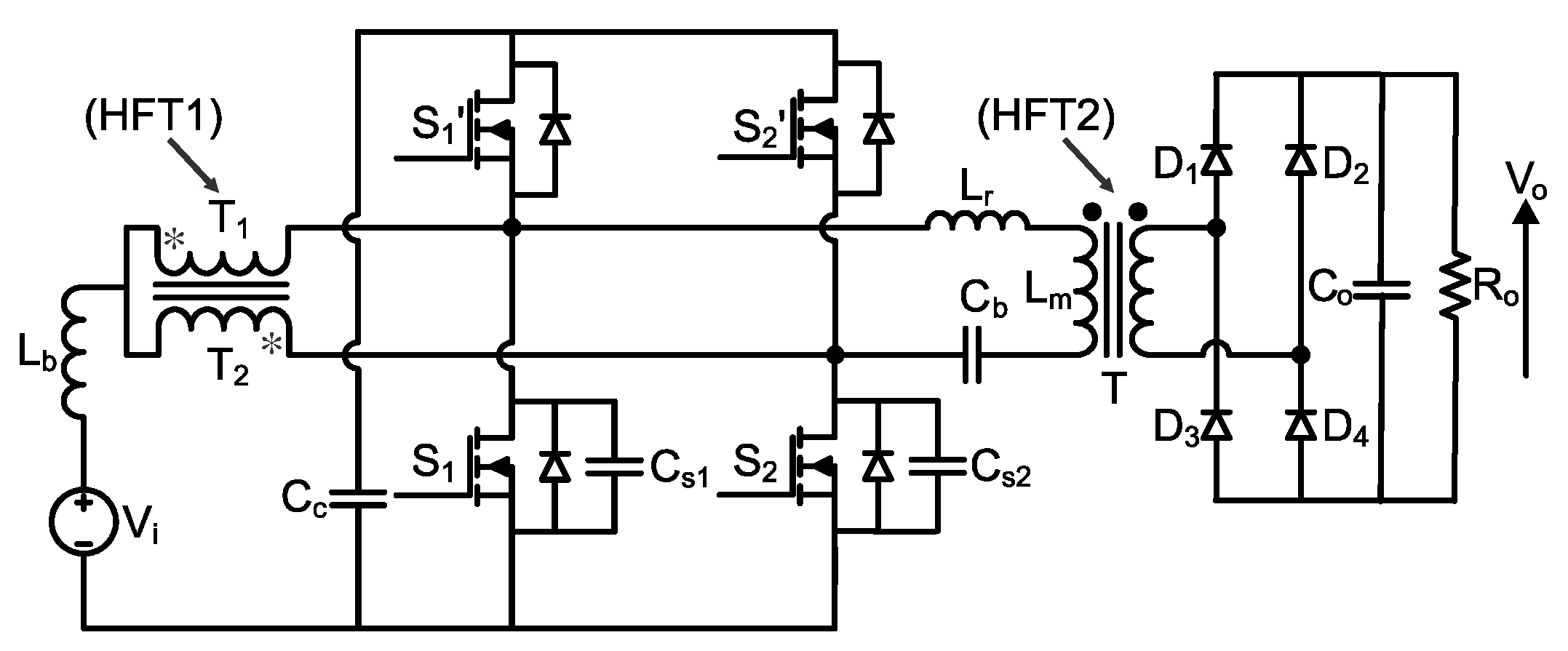
Let us consider a unidirectional version of the topology shown in
Figure 1, which is the focus of the present study. It consists of the dc input voltage source
Vi; the input filter inductor
Lb; the main active switches
S1 and
S2; transformer HFT1, which comprises two primary windings
T1 and
T2 with the same number of turns, while one can add several secondary windings if necessary; transformer HFT2 represented in terms of the magnetizing inductance
Lm; a voltage-doubler rectifier bridge composed of diodes
D1…
D4; the output filter capacitor
Co; and the load
Ro. In turn, the active clamping circuit requires two auxiliary switches
S1′ and
S2′, as well as their respective body diodes; two switching capacitors
Cs1 and
Cs2; one clamping capacitor
Cc; and one resonant inductor
Lr. It is also necessary to connect a blocking capacitor
Cb in series with the primary winding of HFT1 to avoid saturation due to the asymmetric drive signals of the active switches.
One can derive a multiport configuration with inherent design flexibility from
Figure 1 by replacing the secondary-side diodes with active switches aiming to achieve bidirectional power flow. In addition, it is possible to couple multiple secondary windings to transformers HFT1 and HFT2 considering the polarities denoted by “*” and “●”, respectively, resulting in the three-phase architecture shown in
Figure 2. This topology allows for achieving higher power levels, as well as improved distribution of losses and higher power density associated with the magnetics responsible for providing galvanic isolation and multiple regulated outputs. It is worth mentioning that one can replace the loads
Roa and
Rob with photovoltaic (PV) modules, fuel cells, wind turbines, or the conventional ac grid for deriving a multiport structure, for instance [
30]. However, a thorough analysis of the arrangement depicted in
Figure 2 is not part of the scope of this work.
The converter shown in
Figure 1 results from a topological modification of the 3SSC, which is used in the conception of a family of non-isolated dc–dc converters in [
5]. The forthcoming analysis considers that it operates in the steady-state condition and continuous conduction mode (CCM); all power stage elements are ideal; the drive signals of the main switches are overlapped, that is, the duty cycle is
D > 0.5; and the switching frequency is constant.
2.1. Qualitative Analysis
One can analyze the operation of the proposed topology from
Figure 3 and
Figure 4. There are 14 operating stages, but only the first seven will be described here owing to the inherent circuit symmetry.
First stage (
Figure 3a) [
t0,
t1]: Switches
S1 and
S2 are both on. The currents through the primary windings of HFT1 are equal to each other, and the resulting magnetic flux is null. The current through
Lb increases linearly and is equally shared between the branches composed of the transformer windings and the main switches. The output filter capacitor is responsible for supplying the load.
Second stage (
Figure 3b) [
t1,
t2]: Switch
S1 is turned off at
t1, whereas
S2 remains on. The energy stored in
Lr is responsible for charging
Cs1, thus allowing for
S1 to be turned off under ZVS conditions. The drain-source voltage across
S1 increases until it becomes equal to the voltage across
Cc. In addition, there is no energy transfer to the load.
Third stage (
Figure 3c) [
t2,
t3]: The auxiliary switch
S1′ is turned on at
t2. The resonant inductor current flows through the body diode of
S1′ to charge
Cc, until it becomes null at
t3. In this stage, switch
S2 is responsible for ensuring the energy transfer to the load.
Fourth stage (
Figure 3d) [
t3,
t4]: The current through
Lr changes its direction at
t3 and starts flowing through
S1′, while
S2 remains on. Thus, the clamping capacitor supplies energy to the load. The auxiliary switch
S1′ is turned off at
t4, while the energy transfer to the load remains.
Fifth stage (
Figure 3e) [
t4,
t5]: Resonance occurs between
Lr and
Cs1, causing the switching capacitor to be discharged as a consequence. It is noteworthy that one can only turn on
S1 when the voltage across
Cs1 becomes null, which does occur at
t5.
Sixth stage (
Figure 3f) [
t5,
t6]: The body diode of
S1 is forward biased at
t5, and switch
S1 is turned on under ZVS conditions. The diode current decreases until it becomes null at
t6. There is still energy transfer to the load.
Seventh stage (
Figure 3g) [
t6,
t7]: The current starts flowing through
S1 instead of its respective body diode at
t6. It increases until becoming equal to half of the current through
Lb, whereas the energy transfer to the load stops at
t7.
2.2. Quantitative Analysis
Analyzing the instantaneous voltage across
Lb corresponding to
vL(
t) in
Figure 4, one can apply the volt-second balance principle to obtain the voltage gain as in (1).
Figure 5 evidences the influence of the resonant inductance
Lr and the turns ratio of HFT2 corresponding to
a on the voltage gain
G. It is reasonable to state that the gain decreases significantly as the duty cycle increases. Therefore, one should limit the maximum duty cycle in practice to mitigate this inconvenience.
where
Vo is the average output voltage,
Io is the average output current, and
fs is the switching frequency.
One can obtain the theoretical value of the resonant inductance from (2). However, one must also incorporate the leakage inductance of transformer HFT2 represented by
Llkg into the physical design of the resonant inductor while using the value of
Lref in (3) for this purpose. Considering that
Llkg = 0.05⋅
Lm is a conservative estimate, a more accurate design results from measuring
Llkg in the laboratory.
According to [
31], a large clamping capacitor may affect the converter dynamics. To avoid such an inconvenience, one can consider that the resonance period associated with
Lr and
Cc is equal to the switching period
Ts = 1/
fs for simplicity, resulting in (4). The clamping voltage across
Cc is also calculated from (5).
One can determine the input filter inductance from (6).
where Δ
ILb is the peak-to-peak current ripple through
Lb, whose average current is equal to the average input current
Ii.
Transformer HFT1 must be designed while considering half of the output power
Po and a unity turns ratio [
32]. Thus, its respective RMS current
IT1(RMS) and maximum voltage
VT1(max) are given by (7) and (8), respectively.
In turn, transformer HFT2 processes the whole output power. The RMS primary current
IT2p(RMS) and maximum primary voltage
VT2p(max) are calculated from (9) and (10), respectively. Similarly, one can obtain the RMS secondary current
IT2s(RMS) and maximum secondary voltage
VT2s(max) from (11) and (12), respectively.
One can design the blocking capacitor connected in series with the primary winding of HFT2 according to (13).
where Δ
VCb is the peak-to-peak voltage ripple across
Cb as defined by (14).
where
ξ is a constant associated with the primary winding of HFT2, which may be between 0.05 and 0.15 [
32]. It is also worth mentioning that the RMS current through
Cb is
ICb(RMS) =
IT2p(RMS).
The output filter capacitor can be determined from (15), whereas its respective RMS current
ICo(RMS) is calculated from (16).
where Δ
Vo is the peak-to-peak voltage ripple across
Co.
The average and RMS currents through the active switches corresponding to
IS(avg) and
IS(RMS) are calculated from (17) and (18), respectively. One can also determine the maximum voltage
VS(max) from (19).
The average current
ID(avg), the RMS current
ID(RMS), and the maximum voltage
VS1(max) of the rectifier diodes are obtained from (20), (21), and (22), respectively.
2.3. Soft-Switching Conditions
It is necessary to analyze the second and fifth stages represented in
Figure 3b,f, respectively, to ensure the accurate design of the clamping circuit and achieve ZVS of the active switches. During the second stage, the switching capacitor
Cs1 is charged with half of the input current, and the turn-off time is defined by (23).
In turn, the resonance between
Lr and
Cs1 occurs in the fifth stage, resulting in an equivalent circuit represented in terms of (24).
where
vCs1(
t) and
vLr(
t) are the instantaneous voltages across
Cs1 and
Lr, respectively.
Expanding (24) and solving the resulting differential equation, one can obtain
iLr(
t), that is, the instantaneous current through
Lr from (25).
where
ILr0 is the initial current through
Lr, while
ω0 and
Z0 are the angular resonance frequency and the characteristic impedance calculated from (26) and (27), respectively.
f0 being the linear resonance frequency.
Substituting (25) in (24), one can obtain (28). In addition, the voltage across
Cs1 is null at
t =
ton, that is, the instant at which the active switch is turned on. Substituting this condition in (28) yields (29).
Thus, one can determine
ILr0 from the line equation that represents the instantaneous current through
Cc, that is,
iCc(
t) during the interval [
t2,
t4] in
Figure 4, resulting in (30).
Substituting (30) in (29) and normalizing both the turn-on time and the switching frequency as
and
according to (31) and (32), respectively, one can write (33).
Figure 6 shows the behavior of
as a function of
for several values of the duty cycle while considering the ratings adopted for
VCc,
Vo, and
a in the design of an experimental prototype of the converter as described in
Section 4. This plot can be used to design
Cs1 and
Cs2 considering that
corresponds to a small portion of
Ts, e.g., 2%. Thus, one can obtain the corresponding value of
graphically from
Figure 6 and calculate the switching capacitances using (34).
The average and RMS currents through auxiliary switches (
S1′ and
S2′), namely
IS’(avg) and
IS’(RMS), can be calculated from the instantaneous current through
Cc, resulting in (35) and (36). One can also calculate the maximum voltage across an auxiliary switch corresponding to
VS’(max) from (37).
Another important issue lies in determining the load range for which the converter can operate under soft-switching conditions. For this purpose, let us consider that the secondary winding of the high-frequency transformer HFT2 in
Figure 1 is open. The main switches
S1 and
S2, as well as the auxiliary switches
S1′ and
S2′, will operate under ZVS conditions, as ensured by the switching capacitors
Cs1 and
Cs2. The latter elements charge and discharge considering the reactive power flow involving the filter inductor
Lb, the clamping capacitor
Cc, and the magnetizing inductance
Lm.
Figure 7 shows the main waveforms of the converter operating under no-load conditions in terms of the drive signals of the switches, current through
Lb, the current through winding
T1 of transformer HFT1, the magnetizing current through the high-frequency transformer HFT2, the voltage and current on
S1, and the voltage and current on
S1’. Owing to the symmetrical operation of the legs formed by the active switches, the analysis focuses solely on the leg composed of switches
S1 and
S1’. Under no-load conditions, the average current through
Lb is zero. However, its respective RMS value is not null and depends on the current ripple Δ
ILb chosen in the design procedure. One can determine the current ripple from (38), which defines the behavior of the instantaneous voltage across the inductor corresponding to
vLb(
t).
Since
vLb(
t) =
Vi,
diLb(
t) = Δ
ILb, and
t = (
D − 0.5)
Ts, one can write (38) as (39).
The instantaneous currents through
S1 and
S1′ corresponding to
iS1(
t) and
iS1′(
t) can be calculated from (40) and (41), respectively.
where
iLm(
t) is the instantaneous current through the magnetizing current of the high-frequency transformer HFT2.
Neglecting the magnetizing current in (40) and (41), the charging and discharging currents of capacitors
Cs1 and
Cs2 at the turn-on instant
ton and turn-off instant
toff are approximated by (42).
Therefore, the currents through the switches during the switching transitions depend on the inductor current ripple when the converter operates under the no-load condition. Therefore, the converter is capable of achieving soft switching over the entire load range.
2.4. Converter Efficiency
Using well-known equations available in didactic books like [
33,
34], one can calculate the losses in the power stage elements. For instance, the power loss in a diode can be calculated from (43), where the first and second terms of the sum are the conduction and switching losses, respectively.
where
ID(avg) and
ID(RMS) are the average and RMS currents through the diode, respectively;
VD(max) is the maximum voltage across the diode;
VF and
VF(max) are the rated and maximum values of the forward voltage drop, respectively;
rD is the body resistance;
trr is the reverse recovery time; and
Qrr is the reverse recovery charge.
The power loss in a metal-oxide-semiconductor field-effect transistor (MOSFET) can be calculated from (44), where the first and second terms of the sum account for the conduction and switching losses, respectively.
where
Rds(on) is the drain-source on-resistance;
Id(avg) and
Id(RMS) are the average and RMS drain currents, respectively;
Vds(max) is the maximum drain-source voltage;
tr and
tf are the rise time and fall time of the drain current, respectively.
The power loss in an inductor can be obtained from (45), where the first and second terms of the sum are the copper and core losses, respectively.
where
ρCu is the copper resistivity;
lL is the average length of a turn;
NL is the number of turns;
nL is the number of parallel-connected wires;
SL is the cross-sectional area of the conductor;
IL(RMS) is the RMS current through the winding; Δ
B is the magnetic flux variation;
Kh is the hysteresis loss coefficient;
Kf is the eddy-current loss coefficient;
fL is the operating frequency; and
Ve is the core volume.
The power loss in transformer HFT1 can be calculated from (46), where the first and second terms of the sum are the copper and core losses, respectively.
where
lT is the average length of a turn;
NT is the number of turns;
nT is the number of parallel-connected wires;
ST is the cross-sectional area of the conductor; and
IT(RMS) is the RMS current through the winding. It is worth mentioning that a similar equation can be used to calculate the losses in the high-frequency transformer HFT2. However, the number of turns, number of parallel-connected wires, cross-sectional area of the conductor used, and RMS current are not the same for the primary and secondary windings, unlike in HFT1, which has a unity turns ratio.
The power loss in a capacitor can be obtained from (47).
where
RSE is the equivalent series resistance (ESR) of the capacitor and
IC(RMS) is the RMS current through the capacitor.
3. Comparison with Other Push–Pull Converters
Table 1 presents a qualitative comparison among current-fed push–pull converters that rely on active clamping circuits while considering the voltage gain, component count, and stresses on the semiconductors. The topology proposed in [
8] relies on a low component count, but a loss breakdown at the rated power shows that the turn-off losses are somewhat high because the primary-side switches will achieve ZVS only at light load conditions. A similar structure operating at a very high switching frequency is described in [
18], but the conduction losses in the active switches are mainly responsible for degrading the efficiency. The converter in [
21] requires two auxiliary switches while achieving the highest rated power among all compared circuits. The authors claim that the magnetic flux imbalance is not of major concern because the converter uses two clamping capacitors. However, this condition was not assessed experimentally while considering asymmetric gating signals.
The authors in [
23] present a push–pull converter that requires four primary-side switches and one bidirectional switch associated with the secondary winding of the transformer, resulting in a costly and complex arrangement. In turn, the topology in [
24] replaces the diode bridge in the secondary with active switches, while using a proper modulation technique to mitigate voltage spikes on the semiconductors at turn-off. Even though it can achieve voltage clamping naturally, magnetic saturation is still likely to occur. The topology proposed in [
25] also requires a single additional switch, resulting in a simple circuit, but a major drawback is that the voltage gain varies with both the switching frequency and the load even in CCM. Last but not least, it is noteworthy that the introduced active-clamped current-fed push–pull converter is the only one that allows for the connection of a blocking capacitor in series with the primary winding of the transformer to avoid saturation.
4. Experimental Results
Table 2 summarizes the specifications of the experimental prototype represented in
Figure 8. It is also worth mentioning that all waveforms were measured at the rated load condition, while the converter shown in
Figure 1 was designed from the procedure described in
Section 2.
Figure 9 presents the voltage and current waveforms of switch
S1, which can achieve ZVS during turn-on according to the detailed view in
Figure 10. Similarly, the auxiliary switches operate under ZVS conditions during turn-on as demonstrated in
Figure 11 and
Figure 12. It is also noteworthy that there are no voltage spikes on the main and auxiliary switches during turn-on.
Figure 13 shows the waveforms of the clamping capacitor, which is charged and discharged by the current through the resonant inductor. Evidence presented in
Figure 14 shows that the current through one of the primary windings of HFT1 is half of the input current, that is, around 10 A in this case. In turn, the maximum voltage across the rectifier diodes corresponds to the output voltage, that is, 400 V, according to
Figure 15.
Figure 16 compares the efficiency curves of the current-fed push–pull converter employing the active clamping circuit and a passive dissipative snubber. The maximum efficiency is 93.8% and 94.2% at 330 W when using the dissipative snubber and the active clamping circuit, respectively. In turn, the efficiency is 91.8% at the rated power using the proposed solution, that is, 0.6% higher than that obtained with the dissipative snubber.
Figure 17 shows the loss breakdown at the rated load power, which was calculated from the equations presented in
Section 2.4. Since the turn-on losses are negligible, the conduction losses are predominant in the switches. Owing to the limited availability of components in the laboratory, the adopted auxiliary switches are MOSFETs model IRFP460, which have a high drain-source on-resistance of 0.27 Ω. Therefore, it is reasonable to state that there is room for improving the converter efficiency by replacing
S1′ and
S2′ with components with improved characteristics. As for the magnetics, transformer HFT1 accounts for the major portion of losses.
5. Conclusions
This work has presented an active-clamped current-fed dc–dc push–pull converter, which can be arranged as a multiport configuration. Even though the topology employs two high-frequency transformers, it is possible to obtain multiple isolated outputs using both magnetic elements. Unlike most similar structures found in the literature, it allows for connecting a blocking capacitor in series with the primary winding to avoid saturation. Thus, it is not necessary to employ costly and complex control schemes for mitigating the magnetic flux imbalance caused by asymmetrical gating signals applied to the active switches.
The active clamping circuit enables all primary-side switches to operate under ZVS conditions during turn-on. In addition, there are no voltage spikes on the active switches during turn-off, and the resulting switching losses are negligible. Overall, it is reasonable to state that the proposed architecture presents prominent characteristics for applications that require multiport converters and bidirectional power flow.
The results have shown that the operation under soft-switching conditions will yield a higher efficiency over a wide load range when compared with a dissipative snubber, typically used in practical applications. The conduction losses in the active switches account for the major portion of losses, which means that there is room for improvement by choosing MOSFETs with a low drain-source on-resistance. In this sense, future work includes the possibility of not only designing a prototype with optimized components but also exploring a multiport configuration of the converter.

 ,
, 


