
An Experimental EMC Investigation of On-Board Interleaved Buck Converters

Department of Broadband Infocommunications and Electromagnetic Theory, Budapest University of Technology and Economics, Egry József St. 18., 1111 Budapest, Hungary
*
Author to whom correspondence should be addressed.
Energies 2023, 16(9), 3732; https://0-doi-org.brum.beds.ac.uk/10.3390/en16093732
Submission received: 16 March 2023
/
Revised: 24 April 2023
/
Accepted: 25 April 2023
/
Published: 27 April 2023
(This article belongs to the Special Issue Advanced Research on the Control of Power Converters)
Abstract
:On board a satellite, there are different devices that operate from a common energy source called a power bus. Since there are many devices connected to the same power bus and they are in the close vicinity of each other, it is important that they are able to function adequately in the electromagnetic environment of the satellite without introducing intolerable electromagnetic interference to other devices. On-board devices often require voltage levels different from the bus voltage to function, and this is often produced by switching-mode power supplies (SMPS). Their switching-mode operation guarantees that there is less power loss during conversion; however, they also emit conducted and radiated noises into the direction of the power bus and the payloads. In the case of multiple SMPS powered by the same power bus, we can interleave their switching periods. Thus, their noises will cancel each other out on their common input. In this study, we are going to demonstrate the noise reduction of the interleaving method with a setup consisting of two DC-DC converters connected to a simulated power bus.
1. Introduction
In a satellite power system, all on-board payloads and subsystems are fed from a common energy source called a power bus. Since these devices operate from this common network, it is important that the electrical noise emitted from the payloads towards the power bus is kept within certain limits. On board a satellite there can be different types of payloads, e.g., some of them incorporate sensitive electrical measurements, while others produce high frequency radio waves for communication. The electromagnetic compatibility (EMC) of a satellite means that the noise emission of one device does not disturb the operation of others, while said device is able to function in the electromagnetic environment of the satellite. The emission and immunity levels of payloads and how to test these properties at the system level and at the equipment level are all regulated by space technology standards; in the case of missions led by the European Space Agency (ESA), the European Cooperation for Space Standardization (ECSS) EMC standards [1] have to be followed.
On board a satellite, power supplies are used to convert the voltage of the power bus to different voltage levels. Payloads often consist of multiple electronic units with varying input voltage requirements due to their design, and these units also must be galvanically separated from the power bus to prevent failure propagation. For this task, switching-mode power supplies (SMPS) are often used due to their many advantages [2]: they can produce smaller or higher output voltages from the same input voltage, the multiple outputs of one SMPS can be galvanically isolated from each other and, most importantly, they have a much better conversion efficiency compared with linear regulators, which results in much lower mass and volume.
The switching transistor of an SMPS during operation is driven either close to saturation or is completely turned off. Hence, they can transfer power with relatively low power loss. However, the fast rectangular switching action required for good efficiency also produces a wide interference spectrum, which can be a major problem [3]. The conducted noise of an SMPS will propagate in the harness of the power bus, which can lead to radiated noise [4]. There are various techniques that can be used to reduce the noise emission of an SMPS to make it comply with the aforementioned standards. Differential and common mode filters are used to suppress the disturbance caused by the switched-mode currents of converters. To decrease the size and mass of these filter components, the switching frequency of the converters can be increased; however, in this case, the conversion efficiency may also decrease due to higher AC losses [2]. Another method is to interleave the operation of multiple converters, i.e., if two or more converters are connected to the same power bus—such as in a satellite power system—then these converters can be synchronized to the same clock signal, but with different phases [5,6,7,8,9]. In cases with two converters, they will be running on the same switching frequency, but there will be a 180° phase shift between their switch-on times. The input current ripples of the two converters will cancel each other out on the power bus, thus reducing the fundamental and odd harmonic components [10] of the summarized input current spectrum.
In [10], the mathematics of distributed and interleaved systems were thoroughly discussed, including the time-domain and frequency-domain analysis. These analyses give a good insight into how the interleaving method would change the common input current spectrum, i.e., that if we distribute the system into N converters and interleave them, then the fundamental frequency would be N·switching frequency. In [8], simulations were presented for a single-input multiple-output dc-dc converter system. The converters in this work were set to have different duty cycles and output currents, and it was shown that in these conditions the superior solution is to apply uneven phase shifts between the converter input currents. These publications [8,10] give a good theoretical background to the interleaving method. However, experimental setups can be also used, where the nonidealities (e.g., choke inductor value tolerances, uneven phase shift due to the difference of switching device turn-on and turn-off times) can also influence measurement results [7,11]. In [9], similar methods were explored with an experimental setup that was able to reduce the input current ripple through the phase optimization of the switched input currents. The Buck converters presented in [9] were regulated by a four-channel programmable PWM controller. In our paper, we took a different approach for converter regulation and the generation of control signals: the two Buck converters are regulated by individual voltage-mode LM3524 PWM controllers, which are externally synchronized by a dedicated signal generator circuit (see Figure 1). Individual regulation of the converters is necessitated by an ECSS standard issued in [12], which states that externally clocked converters shall deliver output voltages within specifications even in case of loss of the synchronization signal. A similar setup was presented in earlier publications [5,6]; however, an improved version of that setup is presented in this paper. First of all, every circuit, including the converters and the signal generator, was produced on PCBs, which guarantees better repeatability in our measurements compared with the earlier setups. The control scheme of the converters was redesigned, which will be thoroughly explained in the Measurement Setup section. The signal generator went through a total redesign: the circuit comprising CMOS NAND gates and D flip-flops was changed to an ATmega328P microcontroller, which can generate frequency signals above 100 kHz and is also able to set the phase shift between the control signals more accurately. Furthermore, for the isolation of the digital ground we used digital isolators instead of impulse-transformers, since these isolators offer a much more compact and practical solution for this problem. Overall, these modifications improve the noise emission of the system and help in producing more exact measurements.
2. Measurement Methods
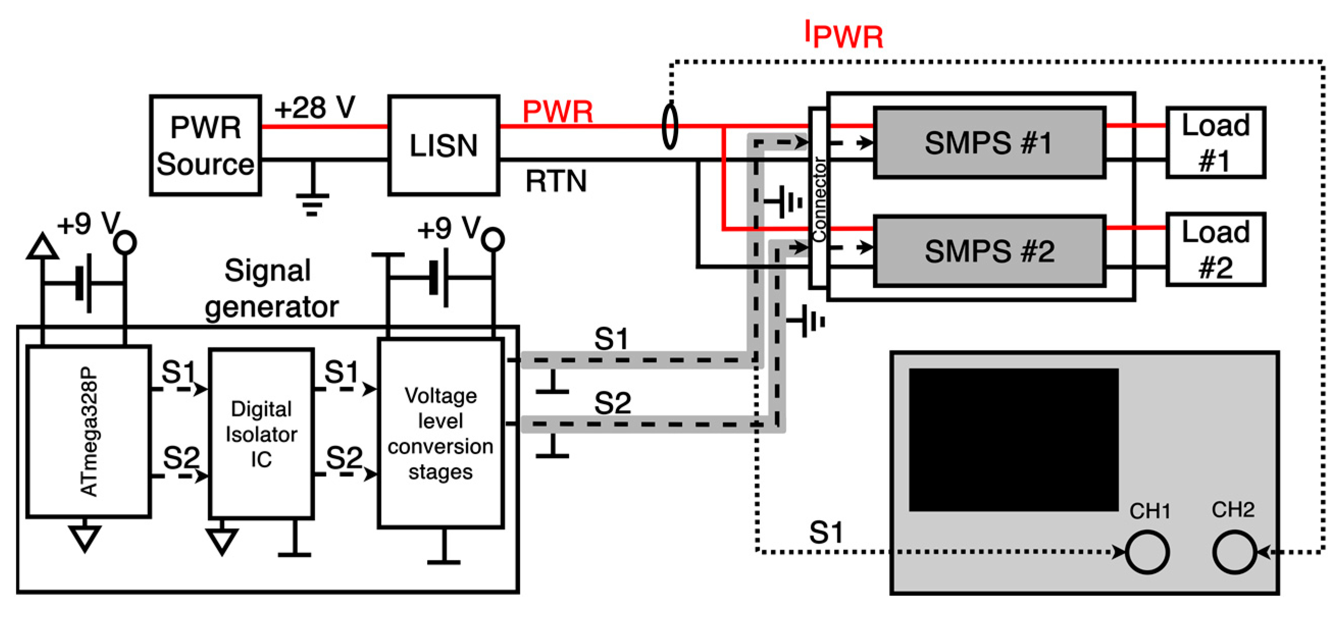
The block diagram of our measurement setup can be seen in Figure 1. The main elements are the simulated power bus, the two SMPS and a dedicated signal generator. In the simulated power bus, a laboratory power supply (PWR source) powers the two SMPS via a Line Impedance Stabilization Network (LISN). The voltage of the PWR line was chosen to be 28 V DC, since this is the typical bus voltage used in satellites below 1.5 kW summarized power level [12]. The task of the LISN was to simulate the impedance of the satellite power bus and to isolate the Buck converters from external conducted disturbances. In these measurements, we did not intend to use any additional filtering excluding the LISN, since our goal was to observe the noise reduction effect of the interleaving method without any other noise suppression techniques. The LISN was made according to the EMC ECSS standard, and its block diagram can be seen in Figure 2 [1,13]. The 1 mF capacitance represents the bus capacitance. The 2 µH coils and the 100 mΩ resistances simulate the series inductance and resistance of the satellite harness. At higher frequencies, the two 1.7 µF capacitances will shunt the 100 kΩ resistors, and the two 50 Ω resistors will be in series, making their sum resistance 100 Ω, which is the typical characteristic impedance of the satellite harness [2].
The conducted emission (CE) of any device can be categorized into differential mode (DM) noise and common mode (CM) noise. The current flowing in the PWR line contains both DM and CM noise currents [14]; the latter typically has a much smaller amplitude than the former. Because of this, the DM current can be taken as equal to the PWR current [15], and to test this theory we will check difference between the CM and PWR current spectrum. The PWR current was measured with a current probe as shown in Figure 1. The current signal was acquired by an R&S HMO1002 Series oscilloscope (Rohde & Schwarz, Munich, Germany); the trigger signal was provided by one of the signal generator outputs. The assembled measurement setup can be seen in Figure 3. To measure the CM current, both the PWR and the RTN lines must be clamped simultaneously [1,5]. For this comparison measurement, a BN150013 (Rohde & Schwarz, Munich, Germany) current probe was used, because it has a large enough clamp to fit through both the PWR and the RTN cables. For other measurements, we used a P6021 (Tektronix, Beaverton, OR, USA) current probe, since in our experience it had better sensitivity in the frequency range between 10 kHz and 1 MHz.
The output current of both converters was 2 A. The power supplies of on-board devices can operate at similar duty cycles, but simultaneously the output power demands can be also different. In [4], there were measurements where the converter loads were asymmetrical, and it was shown that the interleaving method can still yield good results in these conditions.
In our measurements, the switching frequency of both converters was chosen to be 100 kHz, since this is the traditional value used in most ESA missions [16]. We also observed the current spectrum with 200 kHz switching frequency without changing the input and output voltage parameters of the converters.
Frequency-domain measurements are often acquired by spectrum analyzers (SA) or measurement receivers, which are expensive equipment. In [17], it was shown that the CE spectrum of an SMPS can be also obtained by using Fast Fourier Transform algorithm (FFT) on the time-domain measurements of an oscilloscope. The R&S HMO1002 oscilloscope has a built-in FFT analyzer where you can select the measurement time window, the sample number and the transformation window. The sampling frequency was set automatically by the oscilloscope. The resolution of an FFT spectrum can be calculated using the ratio of the sampling frequency and sample number. In the Measurement Results section, the parameters of FFT will be described for each spectrum measurement. Before transformation, the sampled time-domain signal is convolved with a windowing function. The goal of these functions is to reduce spectral leakage caused by the discontinuities at the ends of the analyzed signal. The CE of an SMPS can be time-variant, i.e., the frequency and the amplitude of the harmonics is not stable in time [18]. This is mainly caused by the instability of the switching frequency. To counter the time-variant behavior of the input switched current signal, Hanning-window is a good choice, since it has less amplitude variability due to its smaller scallop loss compared with the rectangular window [18].
An SMPS with a stable switching period will produce narrowband emissions on the fundamental frequency—the switching frequency—and on its harmonics, even beyond 30 MHz, due to the fast risetimes [15]. The standards issued in [1] limit any on-board device emission in a 100 MHz bandwidth, but due to the limitations of the measurement setup we could only investigate in a smaller frequency range. However, the effects of the interleaving for the higher frequency components can still be extrapolated from these measurement results. The spectrum belonging to the interleaved converters case will be compared against the synchronized case where the switch-on times are in phase.
3. Measurement Setup
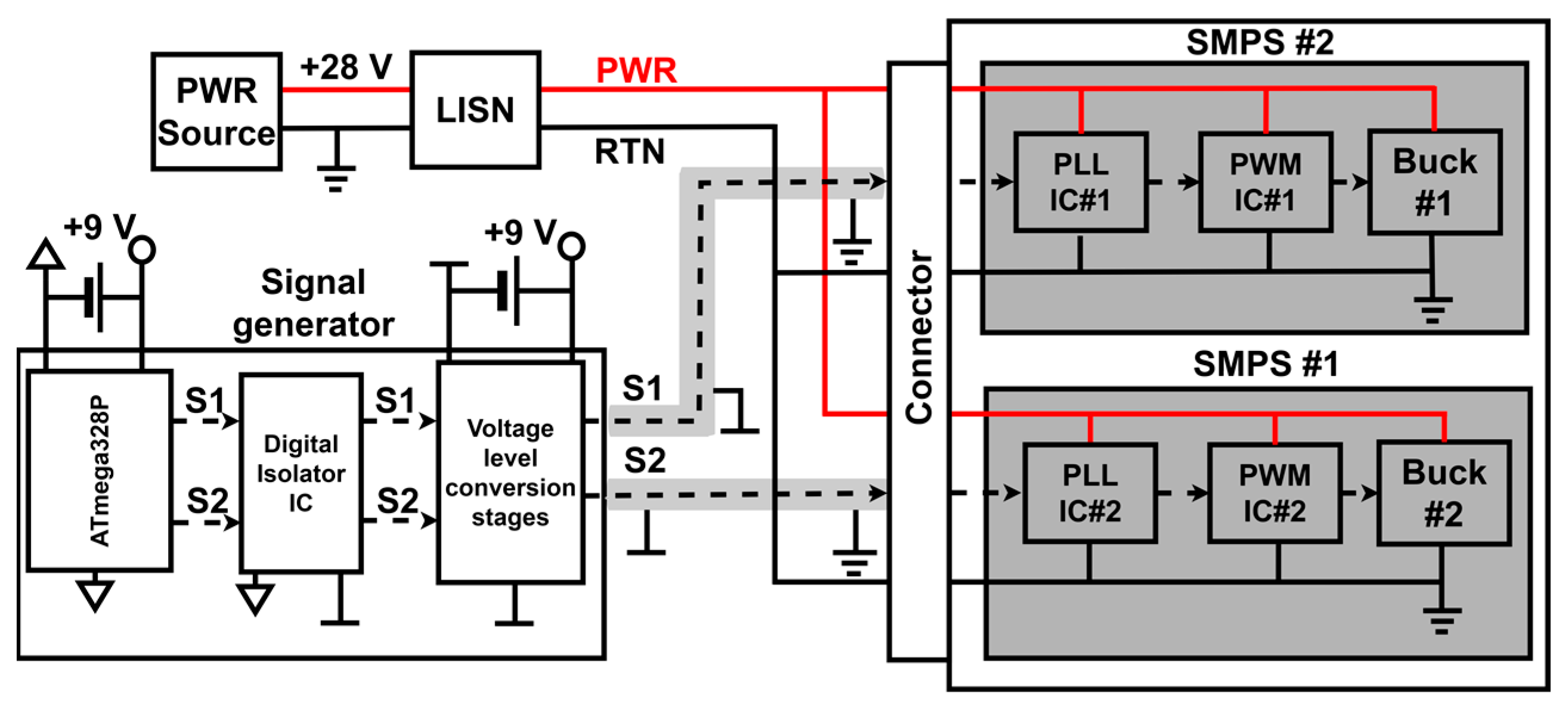
The two SMPS are fix-frequency controlled step-down converters, regulated by individual LM3524 PWM control ICs. The converters can produce 13.4 V output voltage from the 28 V input voltage at a 50 W max power level. In the case of Buck converters, the duty cycle is equal to the ratio of the output and input voltages; in this configuration it was set to ~50%. The structure of the two SMPS circuits can be observed in better detail in Figure 4. From the picture in Figure 4, we can see that the two converters were on the same PCB panel. In Figure 5, we can see how the LM3524 IC was used in this application. The LM3524 has two output transistors with uncommitted collectors and emitters [19]. The T1 and T2 transistors are driven in anti-phase and at half of the OSC signal frequency, and their max duty cycle can be 50%. The output transistor collectors and emitters can be connected in parallel, as shown in Figure 5. Thus, the common collector point controls the FET driver input and the FET switching frequency equals the OSC frequency (see Figure 6). In this configuration, the converter duty cycle can be set between 0% and ~100%.
Both converters have individual Phase-Locked Loops (PLL) which drive the OSC pins of the PWM ICs; thus, the two LM3524s will be externally clocked by the PLLs. The PLL block in Figure 5 synchronizes the S1 or S2 clock signals. For this purpose, the CD4046AE IC was used with its wideband phase comparator mode [20].
The signal generator produces the S1/S2 signals (see Figure 4); the clock signals are generated by the 16-bit Timer/Counter unit of the ATmega328P microcontroller [21], which can set the phase delay between the signals precisely to 0° or to 180°. To isolate the noise of the digital ground from our measurement, digital isolators were used to transmit the S1/S2 signals. In this application, we used a dual channel digital isolator IC (ISO7320FCDR); the inputs of both channels were on the left side and the outputs were on the right side [22]. The ISO7321FCDR also has two channels, but they cannot transmit signals in the same direction, i.e., one channel is the receiver and the other is the transmitter. The other requirement for this IC was that it should be able transmit the relatively low frequency synchronization signal ranging between 100 kHz and 350 kHz (the max oscillator frequency of the LM3524).
The outputs of the digital isolator IC were amplified using the voltage level conversion stages. The PLL ICs in the wideband phase comparator mode can track a signal with a relatively steep rising edge, and the input signal amplitude should swing within CMOS logic levels (1–>70% of VCC and 0–>30% of VCC, where VCC is the power supply voltage of the PLL IC; in this case it was 10 V) [14]. The voltage level conversion stages of the signal generator (see Figure 4) convert the 5 V digital isolator output to a ~9 V voltage level and also ensure an adequate positive edge. In order to avoid ground loop currents, these stages were powered by a +9 V battery and the ground of the signal generator output, and the RTN line was connected at the connector of the panel containing the two SMPS converters.
Overall, the signal generator via the PLLs can synchronize the switching frequency of the converters and can also set the phase delay between their switch-on times.
4. Measurement Results
4.1. Common and Differential Mode Noise Comparison
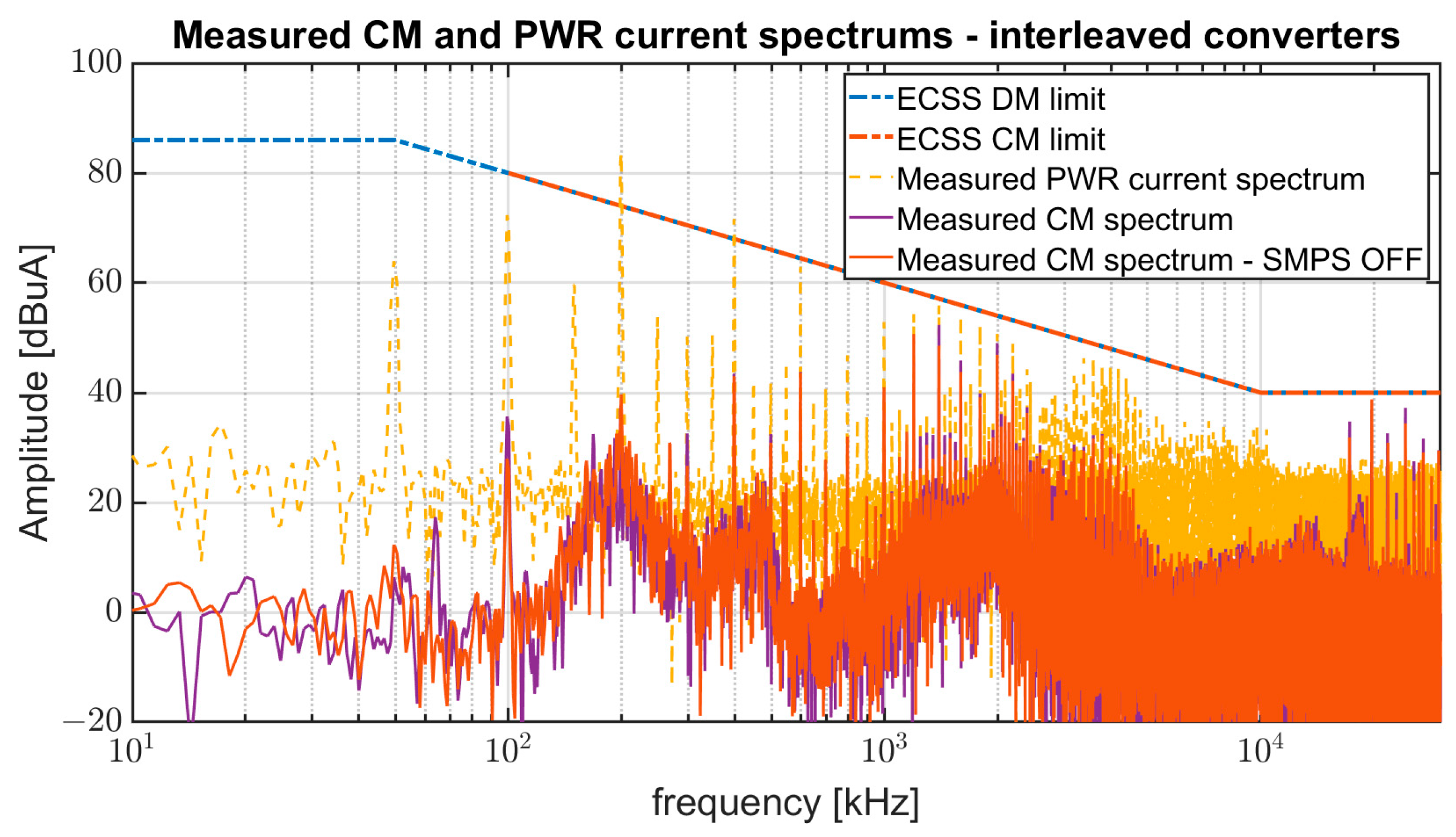
In Figure 7, we can see the CM current spectrum compared to the PWR current spectrum. The CM spectrum was measured in two cases: when the operation of the converters was interleaved (Measured CM spectrum) and when the two converters were turned off (Measured CM spectrum—SMPS off). Since the two spectrums are almost identical and in both cases the amplitude level increases at higher frequencies, we can conclude that the noise emitted by the signal generator capacitively couples into the current flowing in the PWR and RTN lines.
The CM noise was below the PWR current spectrum level—especially at frequencies below 100 kHz—and, because of this, the PWR current can be attributed as DM noise current. The measured spectrums were compared against the ECSS CM and DM limits. The CM spectrums were below the limit, and the PWR current spectrum violated the DM limit at two frequencies—200 kHz and 400 kHz—which were the even harmonic frequencies of the switching frequency.
From this measurement, we can see that the PWR current spectrum consists of narrowband components on the switching frequency and on its harmonics in the frequency range between 50 kHz and 10 MHz. There are components on higher harmonics too, but they are probably below the noise floor of the measurement. In the CM spectrum, peaks can be seen on frequencies over 10 MHz, but they are below the ECSS emission limit.
4.2. PWR Current Spectrum Measurement with Synchronized and Interleaved Converters
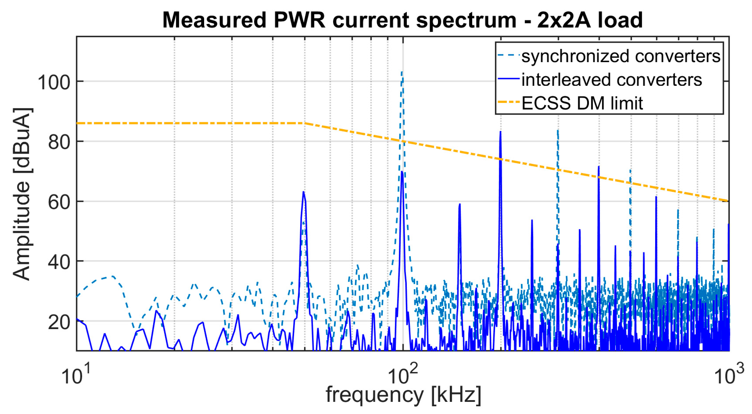
In Figure 8, we can see the PWR current signal in the case of synchronized (0° delay between switch-on times) and interleaved (180° between switch-on times) converters. When the converters are synchronized, their input current ripples are summarized in-phase, resulting in a higher signal amplitude (~150 mApp), and the signal frequency matches the 100 kHz switching frequency of the converters. Due to the interleaving, the signal on the bottom figure has a significantly smaller peak-to-peak value (~15 mApp) and twice as many periods in the same time interval, which means that the signal frequency has increased to 200 kHz. There are small spikes appearing periodically in both signals, which is probably noise coupled from the signal generator.
The signals in Figure 8 were transformed into spectrums, which can be seen in Figure 9. There was a great difference between the two spectrums on the switching frequency component and on its odd harmonics; however, most of the even components were almost identical. In Figure 10, these differences are depicted in better detail. From these diagrams, we can state that with interleaving we can achieve good noise reduction on the switching frequency and its odd harmonics. The even harmonics remained mostly unchanged. Some of them slightly increased due to the interleaving.
From Figure 7 and Figure 9, we can assume that in the case of interleaving it is sufficient to filter the higher even harmonic frequencies, which can be managed with smaller components. In the previous version of this setup [4], we could only achieve 20 dBuA noise reduction on the switching frequency compared with 32.5 dBuA in Figure 9. Since then, a new setup was made for this measurement (see Figure 5). Two major changes were made. One of them was the inclusion of the PLL IC in the SMPS control circuit, which guaranteed smaller phase noise on the S1 and S2 signals; hence, the switching frequency of the converters was more exact. The other major difference was that the generation of the synchronization signals was managed by a microcontroller. In earlier versions, the signal generator circuitry was composed of two flip-flops controlled by a NAND gate RC oscillator [4,5]. The former change had a significant effect on the noise reduction and the latter further enhanced it.
4.3. Measurement Results with Other Switching Frequencies
In Figure 11, we measured the input current ripple of a single SMPS in the case of different switching frequencies. From these measurements, we can see that the input current ripple of an SMPS is inversely proportional to the switching frequency. The ripple is caused by the wiring between the LISN and the SMPS. Since the current ripple is smaller with higher switching frequency, the measured PWR current spectrum should contain smaller narrowband components on the fundamental frequency and its harmonics. In Figure 12, we repeated the measurements of Figure 9, but the switching frequency was increased to 200 kHz. From this figure, we can notice that both spectrums have a better compliance with the ECSS DM limit, as the ones presented in Figure 9 and the measured PWR current spectrum of the interleaved converters in Figure 12 do not violate the standard at all. However, due to the shorter switching periods, the AC losses of the FET and the choke inductor increased, which degrade the conversion efficiency. On the diagram of Figure 13, the conversion efficiency as the function of output current is shown. The two measurement data sets were taken with 100 kHz and 200 kHz switching frequencies. From this comparison, we can conclude that the curve belonging to the higher switching frequency (blue curve, Figure 13) is ~81% at higher current loads, while the other curve is around ~87% at the same output power level.
4.4. Additional Noise of the LM3524 PWM Control IC
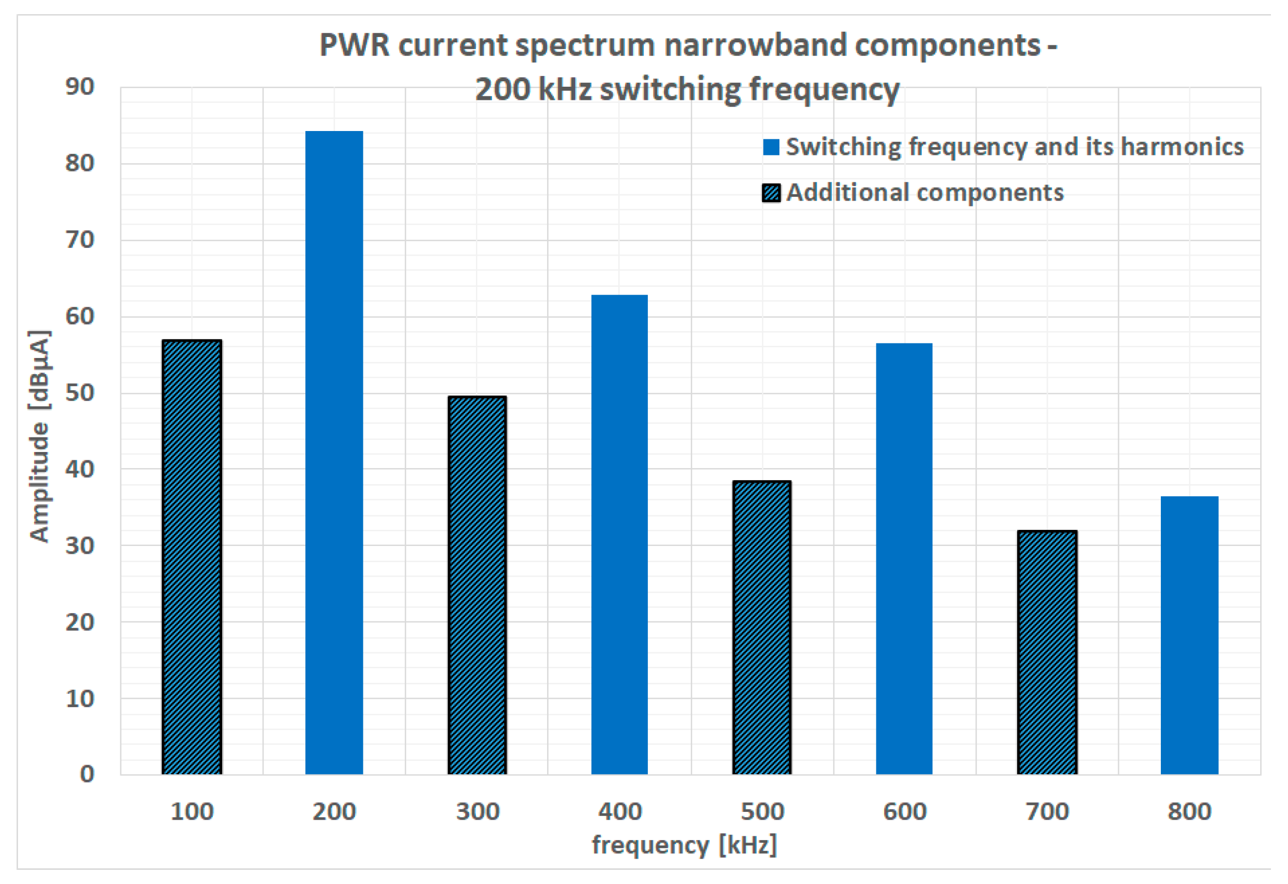
As we mentioned earlier, the PWR current spectrum should only contain narrowband components on the switching frequency and its harmonics. However, if we take a closer look at the spectrums of Figure 7, Figure 9 and Figure 12, we can notice some additional components. In Figure 14 and Figure 15, we listed the narrowband components of the PWR current spectrum from the previous measurements. For the spectrum presented in Figure 14, the switching frequency of the converters was 100 kHz, but we can also see components on half of the switching frequency (50 kHz) and on its odd harmonics (150 kHz, 250 kHz, 350 kHz, etc.). The same phenomenon can be also seen in Figure 15; the converter switching frequency was 200 kHz in this measurement, and there were also additional spectral components on 100 kHz and on its odd harmonics (300 kHz, 500 kHz, 700 kHz, etc.).
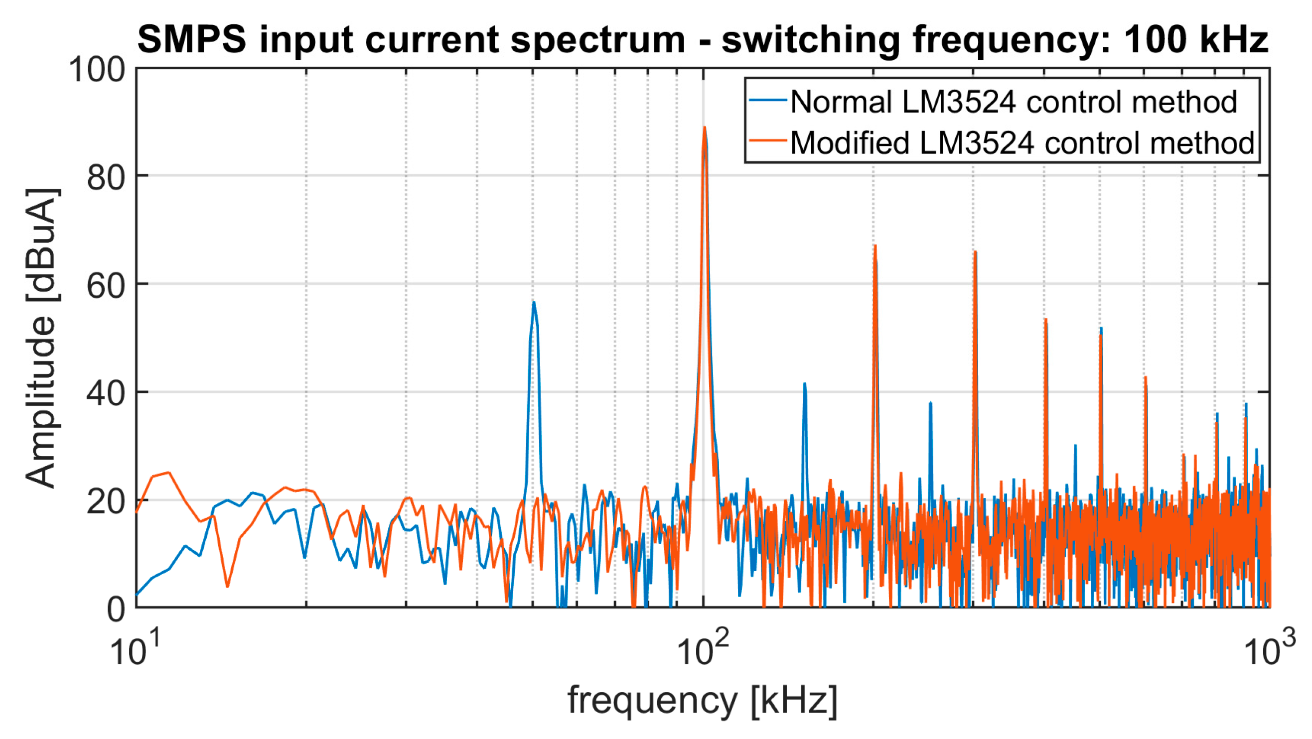
In the Measurement Setup section, we already established that the output transistors of the LM3524 operate at half of the switching frequency, anti-parallel to each other. In this application—as shown in Figure 5—the collectors and the emitters of the output transistors were parallelly connected; thus, the output frequency will match the oscillator signal frequency. One explanation for the additional components shown in Figure 14 and Figure 15 is that the controller outputs will see the common collector point through different impedances and, because of this, there is an additional noise at half of the switching frequency and its harmonics, which couples with the PWR current measurement. To test this theory, we modified the setup so that only one output transistor controlled the FET driver and measured the input current spectrum of only one SMPS. For comparison, we repeated the same measurement with the normal LM3524 control method, as shown in Figure 5. The PWM IC was not externally clocked in either measurement and the converter switching frequency was 100 kHz in both cases. Since the output transistor operates at half of the oscillator frequency, the oscillator had to be set to 200 kHz in the single output case.
In Figure 16, we can see the two spectrums. On the spectrum belonging to the normal control method (blue curve), the additional components appear, but on the other spectrum (orange curve), these components are missing. This proves that our theory was right; the noise was indeed caused by the anti-parallel operation of the LM3524 output transistors. In our oscilloscope measurements, we found that the PWM IC output in the single transistor operation mode cannot be triggered by the oscillator signal, meaning that there is no proper method for externally clocking the two SMPS in the case of single output transistor mode unless we use a different controller IC. For this task, an IC like the UC3823 controller would be suitable, which features a totem-pole output capable of sourcing or sinking the input capacitance of a power MOSFET [23]. This device can also be externally synchronized, and it does not have a second output. Unfortunately, at the time of writing this publication there was no time left to make measurements with this IC, but in the future of this research we wish to replace the LM3524 with the UC3823.
5. Conclusions
In this study, we demonstrated the noise cancellation effect of the interleaving method with a system consisting of two Buck converters and a dedicated signal generator. The measurement results of the improved setup and the earlier setup were compared, and we concluded that the inclusion of the individual PLLs enhanced the noise reduction of the interleaving. The redesign of the signal generator also proved to be successful: the microcontroller can produce signals with exact phase delay and can be reprogrammed for higher frequency signals. There are other microcontrollers that are listed in the ESA Preferred Parts List [24] and which can also be used for the generation of control signals. The digital isolators proved to be a suitable replacement for the impulse-transformers used in the earlier version of the signal generator [5,6]: with these ICs, we could isolate the digital and power supply grounds, and they also required less design considerations compared with impulse transformers.
We have also shown that with higher switching frequencies we can achieve smaller noise emission. However, the conversion efficiency also decreased. When designing a power supply, one has to keep in mind that component selection is crucial, e.g., for higher switching frequencies, power MOSFETs with shorter turn-on and turn-off speeds should be used.
From the analysis of CE spectrums, we concluded that there were other additional components besides the switching frequency component and its harmonics. These additional components were caused by the anti-phase operation of the LM3524 output transistors. Since these controllers cannot be externally synchronized in single output transistor mode, we had to a find a suitable replacement controller IC, which does not have multiple output transistors, e.g., the UC3823 high-speed PWM controller.
In further continuation of this research, we plan to test the interleaving method with a setup consisting of four Buck converters. The four converters can be separated into two pairs, the operation of individual converters in a pair can be synchronized and the operation of the pairs can be interleaved. The other possibility is to have four converters with 25% duty cycle and with 90 degree phase shift between their operation. There are other variations with different duty cycles and output current loads that can be analyzed.
In [25,26], we could also see setups with parallel converters, where the aim of the research was to reduce output voltage ripple. The electrical power system (EPS) of a satellite incorporates multiple paralleled converters (array power regulators—APRs), which transfer energy from the solar panels to the power bus during sunlight [16]. These converters employ Maximum Power Point Tracker algorithms, which optimize the duty cycle of APRs so that the max output power is gained from the solar panels. In an EPS, there is an MPPT converter for each solar array [27] and their outputs are parallelly connected; their common output is the power bus. The operation of these converters can be interleaved, greatly reducing the output voltage ripple and thus easing the requirements on the capacitor bank of the EPS. The setup presented in our work can be used to make such measurements with the extension of a circuit consisting of four diodes, which will summarize the regulated outputs of the converters.
Author Contributions
Conceptualization, T.K.; methodology, T.K.; software, T.K.; validation, L.N. and T.K.; formal analysis, T.K.; investigation, T.K.; resources, L.N.; data curation, T.K.; writing—original draft preparation, T.K.; writing—review and editing, L.N.; visualization, T.K.; supervision, L.N.; project administration, L.N. All authors have read and agreed to the published version of the manuscript.
Funding
This research received no external funding.
Data Availability Statement
Not applicable.
Conflicts of Interest
The authors declare no conflict of interest.
References
- ECSS-E-ST-20-07C Rev2, Space Engineering, Electromagnetic Compatibility; European Cooperation for Space Standardization (ECSS): Noordwijk, Netherlands, January 2022. Available online: https://ecss.nl/standard/ecss-e-st-20-07c-rev-2-electromagnetic-compatibility-3-january-2022/ (accessed on 1 February 2023).
- Pressman, A.I.; Billings, K.; Morey, T. Switching Power Supply Design, 3rd ed.; McGraw Hill: New York, NY, USA, 2009. [Google Scholar]
- Billings, K.; Morey, T. Switchmode Power Supply Handbook, 3rd ed.; McGraw Hill: New York, NY, USA, 2010. [Google Scholar]
- Spadacini, G.; Grassi, F.; Bellan, D.; Pignari, S.A.; Marliani, F. Prediction of Conducted Emissions in Satellite Power Buses. Int. J. Aerosp. Eng. 2015, 2015, 601426. [Google Scholar] [CrossRef]
- Tamás, K.; Lajos, N. Conducted Emission Measurement of Interleaved DC-DC Buck Converters. In Proceedings of the 2022 ESA Workshop on Aerospace EMC (Aerospace EMC), Virtual, 23–25 May 2022; pp. 1–5. [Google Scholar] [CrossRef]
- Tamás, K.; Lajos, N. Conducted Emission simulation and measurement of interleaved DC-DC converters. Infocommun. J. 2022, XIV, 39–43. [Google Scholar]
- Zumel, P.; Garcia, O.; Cobos, J.A.; Uceda, J. EMI reduction by interleaving of power converters. In Proceedings of the Nineteenth Annual IEEE Applied Power Electronics Conference and Exposition, 2004. APEC’04, Anaheim, CA, USA, 22–26 February 2004; Volume 2, pp. 688–694. [Google Scholar] [CrossRef]
- Schuck, M.; Pilawa-Podgurski, R.C.N. Input current ripple reduction through interleaving in single-supply multiple-output dc-dc converters. In Proceedings of the 2013 IEEE 14th Workshop on Control and Modeling for Power Electronics (COMPEL), Salt Lake City, UT, USA, 23–26 June 2013; pp. 1–5. [Google Scholar] [CrossRef]
- Weinstein, J.; Huerta, S.C.; Zhao, Z.; Mincey, J.; Moussaoui, Z. Optimized phase positioning for minimizing input filter requirements in single-input multiple-output DC-DC switch-mode power supplies. In Proceedings of the 2014 IEEE Applied Power Electronics Conference and Exposition—APEC 2014, Fort Worth, TX, USA, 16–20 March 2014; pp. 455–459. [Google Scholar] [CrossRef]
- Ozeri, S.; Shmilovitz, D.; Singer, S.; Martinez-Salamero, L. The Mathematical Foundation of Distributed Interleaved Systems. IEEE Trans. Circuits Syst. I Regul. Pap. 2007, 54, 610–619. [Google Scholar] [CrossRef]
- Antoszczuk, P.D.; Retegui, R.G.; Wassinger, N.; Maestri, S.; Funes, M.; Benedetti, M. Characterization of Steady-State Current Ripple in Interleaved Power Converters Under Inductance Mismatches. IEEE Trans. Power Electron. 2014, 29, 1840–1849. [Google Scholar] [CrossRef]
- ECSS-E-ST-20C-Rev. 1, Space Engineering Electrical and Electronic; European Cooperation for Space Standardization (ECSS): Noordwijk, The Netherlands, 2019; Available online: https://ecss.nl/standard/ecss-e-st-20c-rev-1-electrical-and-electronic-15-october-2019/ (accessed on 4 April 2023).
- Ádám, F. EMC Analysis of the Charge Density Meter for Satellite On-Board Application (ESEO-LMP). BSc Thesis, Department of Broadband Infocommunications and Electromagnetic Theory, Budapest University of Technology and Economics, Budapest, Hungary, 2016. [Google Scholar]
- PÉrez, A.; SÁnchez, A.-M.; ReguÉ, J.-R.; RibÓ, M.; RodrÍguez-Cepeda, P.; Pajares, F.-J. Characterization of Power-Line Filters and Electronic Equipment for Prediction of Conducted Emissions. IEEE Trans. Electromagn. Compat. 2008, 50, 577–585. [Google Scholar] [CrossRef]
- Williams, T. EMC for Product Designers, 4th ed.; Elsevier: Amsterdam, The Netherlands, 2007. [Google Scholar]
- Mourra, O.; Fernandez, A.; Tonicello, F. Buck Boost Regulator (B2R) for spacecraft Solar Array Power conversion. In Proceedings of the 2010 Twenty-Fifth Annual IEEE Applied Power Electronics Conference and Exposition (APEC), Palm Springs, CA, USA, 21–25 February 2010; pp. 1313–1319. [Google Scholar] [CrossRef]
- Sánchez, A.-M.; Pignari, S.A.; Regué, J.-R.; Ribó, M. Device Modeling for Nonstationary Conducted Emissions Based on Frequency- and Time-Domain Measurements. IEEE Trans. Electromagn. Compat. 2012, 54, 738–746. [Google Scholar] [CrossRef]
- Bellan, D.; Marliani, F.; Pignari, S.A.; Spadacini, G. Spectral analysis of conducted emissions of DC/DC converters. In Proceedings of the 2010 IEEE International Symposium on Electromagnetic Compatibility, Fort Lauderdale, FL, USA, 25–30 July 2010; pp. 490–494. [Google Scholar] [CrossRef]
- LM2524D/LM3524D Regulating Pulse Width Modulator Datasheet (Rev. E.); Texas Instruments: Dallas, TX, USA, 2022.
- Morgan, D.K. CD4046B Phase-Locked Loop: A Versatile Building Block for Micropower Digital and Analog Applications; Application Report; Texas Instruments: Dallas, TX, USA, 2003. [Google Scholar]
- Atmel 7810 Automotive Microcontrollers ATmega328P Datasheet, Microchip. pp. 89–113. Available online: https://www.microchip.com/en-us/product/ATmega328P (accessed on 4 April 2023).
- ISO732x Robust EMC, Low Power, Dual-Channel Digital Isolators Datasheet (Rev. C), Texas Instrument. Available online: https://www.ti.com/product/ISO7320FC/part-details/ISO7320FCDR (accessed on 4 April 2023).
- UC3823 High Speed PWM Controller Datasheet; Texas Instruments: Dallas, TX, USA, 2007.
- European Preferred Parts List (EPPL), ESCC/RP/EPPL007-46 (REP 007), January 2023. Available online: https://escies.org/webdocument/showArticle?id=166 (accessed on 5 April 2023).
- Perreault, D.J.; Kassakian, J.G. Distributed interleaving of paralleled power converters. IEEE Trans. Circuits Syst. I Fundam. Theory Appl. 1997, 44, 728–734. [Google Scholar] [CrossRef]
- Sefa, İ.; Özdemir, Ş. Experimental study of interleaved MPPT converter for PV systems. In Proceedings of the 2009 35th Annual Conference of IEEE Industrial Electronics, Porto, Portugal, 3–5 November 2009; pp. 456–461. [Google Scholar] [CrossRef]
- Bifaretti, S.; Pipolo, S.; Catalano, T.F.; Daprati, G.; Iacovone, V.; Scione, E. Functional Study of a Distributed MPPT Power Management System. E3S Web Conf. 2017, 16, 13008. [Google Scholar] [CrossRef]
Figure 1.
PWR current measurement setup.

Figure 2.
LISN block diagram.

Figure 3.
Assembled PWR current measurement setup.

Figure 4.
EMC measurement setup block diagram.

Figure 5.
LM3524 IC application in step-down converters.

Figure 6.
LM3524 control signals.

Figure 7.
PWR current spectrum and CM current spectrum comparison, measured with R&S BN150013 current probe, frequency span: 30 MHz, sampling rate: 62.5 MSa/s, sample number: 65536.
Figure 7.
PWR current spectrum and CM current spectrum comparison, measured with R&S BN150013 current probe, frequency span: 30 MHz, sampling rate: 62.5 MSa/s, sample number: 65536.

Figure 8.
PWR current signal—synchronized converters (top figure), interleaved converters (bottom figure), measured with Tektronix P6021 current probe.
Figure 8.
PWR current signal—synchronized converters (top figure), interleaved converters (bottom figure), measured with Tektronix P6021 current probe.

Figure 9.
PWR current spectrum—synchronized converters and interleaved converters, measured with Tektronix P6021 current probe, frequency span: 1 MHz, sampling rate: 6.25 MSa/s, sample number: 8192, sample window: 1.31 ms.
Figure 9.
PWR current spectrum—synchronized converters and interleaved converters, measured with Tektronix P6021 current probe, frequency span: 1 MHz, sampling rate: 6.25 MSa/s, sample number: 8192, sample window: 1.31 ms.

Figure 10.
PWR current spectrum—comparison of even and odd harmonic components of the signal.

Figure 11.
Measured SMPS current input signal with different switching frequencies, measured with Tektronix P6021 current probe.
Figure 11.
Measured SMPS current input signal with different switching frequencies, measured with Tektronix P6021 current probe.

Figure 12.
PWR current spectrum—synchronized converters and interleaved converters, measured with Tektronix P6021 current probe, frequency span: 6 MHz, sampling rate: 12.5 MSa/s, sample number: 16384, sample window: 1.31 ms.
Figure 12.
PWR current spectrum—synchronized converters and interleaved converters, measured with Tektronix P6021 current probe, frequency span: 6 MHz, sampling rate: 12.5 MSa/s, sample number: 16384, sample window: 1.31 ms.

Figure 13.
Conversion efficiency in the case of different switching frequencies, 28 V input voltage, 13.5 V output voltage.
Figure 13.
Conversion efficiency in the case of different switching frequencies, 28 V input voltage, 13.5 V output voltage.

Figure 14.
PWR current spectrum narrowband components—interleaved converters, switching frequency: 100 kHz.
Figure 14.
PWR current spectrum narrowband components—interleaved converters, switching frequency: 100 kHz.

Figure 15.
PWR current spectrum narrowband components—synchronized converters, switching frequency: 200 kHz.
Figure 15.
PWR current spectrum narrowband components—synchronized converters, switching frequency: 200 kHz.

Figure 16.
SMPS input current spectrum, converter switching frequency: 100 kHz, measured with Tektronix P6021 current probe, frequency span: 1 MHz, sampling rate: 6.25 MSa/s, sample number: 8192.
Figure 16.
SMPS input current spectrum, converter switching frequency: 100 kHz, measured with Tektronix P6021 current probe, frequency span: 1 MHz, sampling rate: 6.25 MSa/s, sample number: 8192.

Disclaimer/Publisher’s Note: The statements, opinions and data contained in all publications are solely those of the individual author(s) and contributor(s) and not of MDPI and/or the editor(s). MDPI and/or the editor(s) disclaim responsibility for any injury to people or property resulting from any ideas, methods, instructions or products referred to in the content. |
© 2023 by the authors. Licensee MDPI, Basel, Switzerland. This article is an open access article distributed under the terms and conditions of the Creative Commons Attribution (CC BY) license (https://creativecommons.org/licenses/by/4.0/).
Share and Cite
MDPI and ACS Style
Nagy, L.; Kőnig, T. An Experimental EMC Investigation of On-Board Interleaved Buck Converters. Energies 2023, 16, 3732. https://0-doi-org.brum.beds.ac.uk/10.3390/en16093732
AMA Style
Nagy L, Kőnig T. An Experimental EMC Investigation of On-Board Interleaved Buck Converters. Energies. 2023; 16(9):3732. https://0-doi-org.brum.beds.ac.uk/10.3390/en16093732
Chicago/Turabian StyleNagy, Lajos, and Tamás Kőnig. 2023. "An Experimental EMC Investigation of On-Board Interleaved Buck Converters" Energies 16, no. 9: 3732. https://0-doi-org.brum.beds.ac.uk/10.3390/en16093732
Note that from the first issue of 2016, this journal uses article numbers instead of page numbers. See further details here.