Article

Autonomous Gate Drivers Tailored for Triangular Current Mode-Based Zero-Voltage Switching Two-Level Three-Phase Inverters for Electric Vehicle Drive Systems

School of Electrical Engineering and Computer Science, KTH Royal Institute of Technology, 11428 Stockholm, Sweden
*
Author to whom correspondence should be addressed.
Submission received: 1 February 2024 / Revised: 13 February 2024 / Accepted: 21 February 2024 / Published: 23 February 2024
(This article belongs to the Special Issue Modeling, Control and Design of Power Electronics Converters)

Abstract

:
The demand for highly efficient and dynamic electric vehicles (EVs) has increased dramatically. The traction inverter, a pivotal component in an EV powertrain, plays a crucial role. This study is dedicated to designing a traction inverter with focus on achieving high efficiency and elevated power density and mitigating electromagnetic interference (EMI) issues. To realize these objectives, autonomous gate drivers (AGDs) are proposed and designed using LTspice simulation software. The aim is to achieve zero voltage switching (ZVS) at both turn-on and turn-off through the utilization of triangular current mode (TCM) control on the gate driver. The AGDs implement a current modulation scheme by sensing the current and voltage and generating gate-source voltage signals with minimal delays. The implemented current modulation scheme by the AGDs results in an efficiency exceeding 99% for a 10 kW power rating. The sinusoidal output waveforms not only contribute to extending the motor lifespan by mitigating sharp-edge voltages but also bring advantages such as reduced switch stress, decreased EMI, and simplified thermal management.

1. Introduction

One of humanity’s greatest challenges is to develop sustainable transportation concepts. The electric road vehicle stands out as one of the most important alternatives, but it comes with challenges related to energy storage, energy distribution, power conversion, heat dissipation, power cycling, electromagnetic interference (EMI), reliability, compactness, and cost. The efficiency of power converters is not only important for saving energy; managing heat dissipation on a vehicle is equally critical, whether it operates in hot or cold environments. Creating competitive and efficient power converters for such vehicles is among the most crucial aspects to address.
The electric vehicle (EV) battery, primarily lithium-ion [1], acts as the key energy storage unit essential for efficient EV functionality. Although lithium-ion batteries are prevalent, emerging options such as solid-state [2] and lithium–sulfur batteries [3] hold promise for improving efficiency and extending range.
One of the key components of an EV powertrain is the traction inverter, responsible for converting DC power from the battery into AC power to drive the electric motor(s). From a car manufacturer’s point of view, a traction inverter should be energy-efficient, compact, reliable, highly dynamic, and cost-effective. These requirements pose several conflicts with design targets because, for instance, energy efficiency and cost call for almost opposite solutions. Similar trade-offs usually have to be made regarding compactness and cost. There is a demand for high power density, which enhances the overall vehicle dynamics, and high efficiency, which increases the driving range of the vehicle [4].
To achieve high power density and low cost, one possibility is to reduce the DC-link capacitor of the traction inverter by allowing a very high voltage ripple. This was shown for a 15 kW inverter with a 10 µF DC-link capacitor in [5]. The problem with this concept is, however, that EMI increases on both the input and output. Another approach is to reduce the size and volume of filtering components, ensuring compliance with EMI regulations by increasing the switching frequency of the power devices [6].
Inverters employing silicon insulated-gate bipolar transistors (IGBTs) as power switching devices featuring a blocking voltage of 1200 V dominate the business today. However, IGBTs show high switching losses attributed to bipolar on-state carriers, leading to conductivity modulation lag during turn-on and tail currents during turn-off [7]. Consequently, these high switching losses impose limitations on the switching frequency of inverters utilizing IGBTs, typically ranging from 5 to 20 kHz [8].
At present, silicon carbide (SiC) power electronics have significant advantages to offer for the electric vehicle business [9]. SiC metal-oxide semiconductor field-effect transistors (MOSFETs) enable reduced chip sizes, lower switching losses due to their unipolar carrier characteristic [10], reduced conduction losses with the help of fundamental material improvements [11], and operation at a higher switching frequency up to a hundred kHz or more [12], which reduces the required capacitance/size of the DC-link capacitor and increases power density [13]. By enabling extremely energy efficient and compact power conversion, and better thermal performance than for the silicon counterpart, dramatic volume reductions are possible, which enables considerable freedom to design an overall better vehicle. However, high-speed switching (which is possible with SiC power electronics) is also associated with EMI issues [13].
EMI poses a significant challenge to the reliable operation of EVs, affecting various components such as power electronics [14], electric motors, and charging systems [15]. To address EMI and reduce its impact, strategies like shielding, EMI filters, proper grounding, component isolation, and layout design optimization are essential [16]. Adhering to electromagnetic compatibility [17] standards further enhances reliability. To reduce the EMI issues in the inverter, soft-switching power converters are often employed.
Soft-switching (SSW) [18] power converters help to maintain low switching losses even at high switching frequencies, which increases the overall efficiency and reliability of the system. Soft switching can be achieved by zero-voltage switching (ZVS) and/or zero-current switching (ZCS). ZVS occurs when the voltage across the switch is made zero by prior conduction of the body diode of the MOSFET and by using a capacitive snubber at turn-off [19]. A ZVS technique is used to allow high-frequency operation and minimize both the noise and switching losses. ZCS results when the current across the switch is made zero and then allows the switch to turn off at zero-current.
In converter operation, there are three modes of filter inductor current. The first one is the continuous conduction mode (CCM) in which the filter inductor current remains positive. The hard switching in CCM results when the output capacitance ( C d s ) discharges into the switching element during turn-on. The CCM provides the advantage of reduced stress on the inductor current. However, it comes with the drawback of larger size for the inductor and capacitor filter components, resulting in a bulkier system. The second mode is the discontinuous conduction mode (DCM), in which the inductance of the inductor is taken low beyond a limit that makes the current zero, which results in ZCS [20,21]. The third mode is the triangular current mode (TCM) [22], in which the filter inductor current comprises both positive and negative peaks which helps in achieving turn-on ZVS for both high-side and low-side switches in a half-bridge configuration [6]. The TCM is also known as critical conduction mode (CRM) [23] and/or boundary conduction mode (BCM) [24].
The concept of TCM operation has been proposed to attain ZVS in clamped-voltage concepts for flyback converters [19], power factor correction [21,25,26], as well as in three-phase rectifiers [27], inverters [28,29,30,31], and bidirectional converters [31,32].
In three-phase AC/DC or DC/AC applications, achieving ZVS can be accomplished either with auxiliary circuits [33] or without auxiliary circuits [22]. Techniques that eliminate the need for auxiliary circuits are gaining more attention due to their simplicity, and one such method is the TCM. In the context of three-phase four-wire applications, TCM can be adopted to achieve ZVS like single-phase converters, benefiting from the effective decoupling of the three phases [28]. For three-wire applications, implementing TCM in all three phases within a conventional topology (e.g., a two-level voltage source inverter) is challenging since the sum of three-phase currents must be zero. As proposed in [28], decoupling the three phases using capacitors enables the implementation of TCM.
TCM modulation provides significant advantages in achieving both high efficiency and high power density simultaneously [34]. The large ripple in the inductor current offers two advantages: a reduced inductance value, minimizing the volume of the filter inductor, and the presence of positive and negative currents, aiding in achieving ZVS during turn-on and turn-off (if capacitive snubbers are employed) for both high-side and low-side switches in a half-bridge configuration [6]. The rms current in TCM is approximately 15% higher than in CCM, resulting in around a 30% increase in conduction losses [34]. The increase in conduction losses can be counterbalanced by the significant decrease in switching losses at high switching frequencies. This allows for efficient operation at frequencies exceeding 100 kHz, ultimately achieving the intended high power density. An additional way to counterbalance the increase in conduction losses is to increase the chip area, which reduces conduction losses [35], increases cooling capability, and increases effective snubber capacitance through increased parasitic output capacitance of the SiC MOSFETs. The latter may significantly reduce the switching losses (except at very low current levels).
To achieve ZVS in the TCM mode, the control of the main power circuit is executed through the implementation of digital signal processing devices, such as DSPs and FPGAs, along with sensing circuits [34,36].
This research aims to design AGDs for TCM-based ZVS three-phase inverters without using any digital signal processing devices for the modulation and current control. However, such devices may have to be used to determine the reference values for the AGDs, but these tasks require much lower bandwidth. The tasks of the AGDs are:
  • Achieve turn-on ZVS by sensing the on-state of the power device on the gate driver.
  • High-speed peak current control by measuring the current of the power device on the gate driver.
To ensure optimal converter performance, precise timing without delays is important for the power electronic switches. Traditional methods involve the measurement of voltage and current and then sending signals to a controller for decision-making, and then transmitting switching signals to the gate drivers. This can introduce significant delays, affecting the soft-switching implementation. In contrast, measuring voltage and current directly at the gate driver minimizes these delays, allowing for autonomous operation of the gate driver for modulation of the converter. However, to determine when the power electronic switches should turn off, a galvanically isolated current reference must be sent to the gate driver. This isolation is achieved through a galvanically isolated current sensor functioning as a signal transmission device. The elegance of this concept lies in the fact that the required bandwidth for the current reference is significantly lower than that needed for measuring the actual switch current.
The proposed AGDs offer several advantages to three-phase inverters, including a simple topology, a current modulation scheme, high power density due to a high switching frequency and small filter inductor, integration of the controller on the gate driver, high efficiency by minimizing time delays, and achieving ZVS at both turn-on and turn-off. Additionally, there is a mitigation of EMI due to sinusoidal output current and voltage waveforms.
The key contributions of this paper are:
  • Analyzing the intended operation of the proposed AGDs for a 10 kW power-rated inverter.
  • Examining ZVS at both turn-on and turn-off by computing the switching losses.
  • Analyzing the sinusoidal output waveforms of currents and voltages.
  • Evaluating the inverter efficiency based on the proposed AGDs.
  • Assessing the adaptive control features of the proposed AGDs.
The paper is structured as follows: Section 2 introduces the topology and operating principle of the inverter. Section 3 delves into the details of the proposed AGDs. Section 4 presents the simulation results and discussion. Section 5 concludes the article. Section 6 outlines the future work.

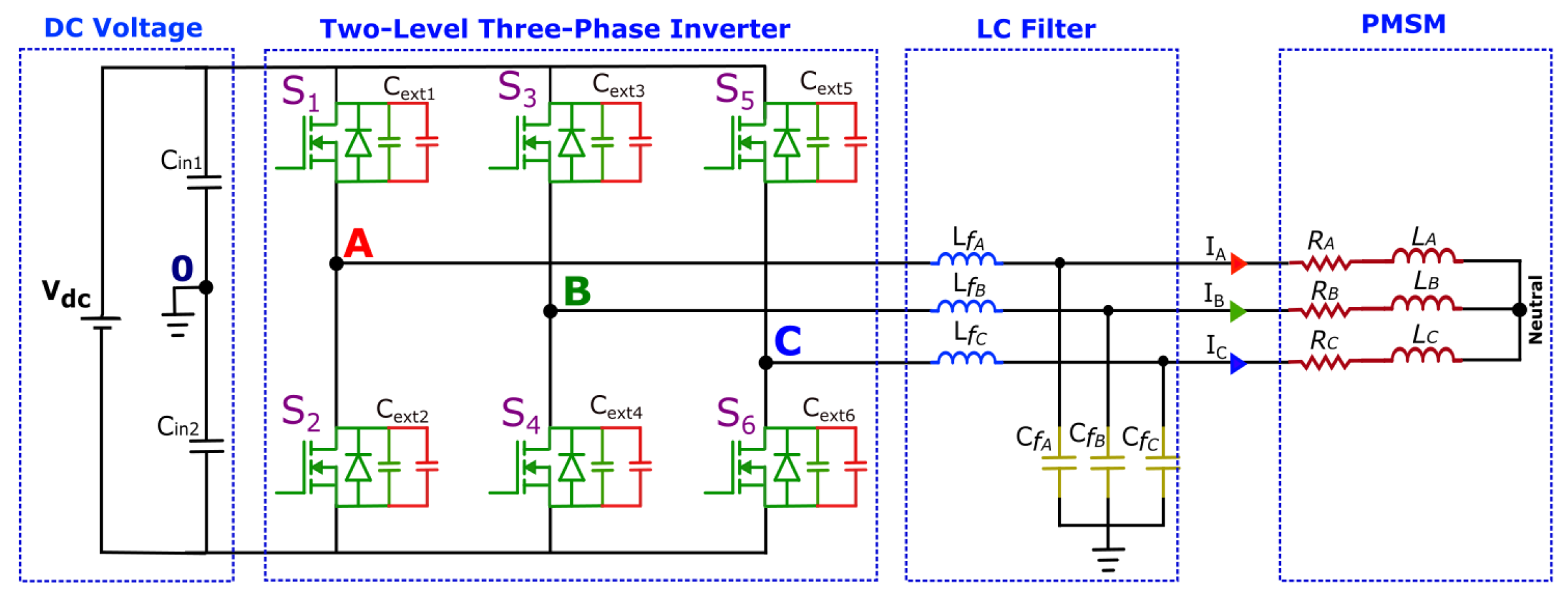
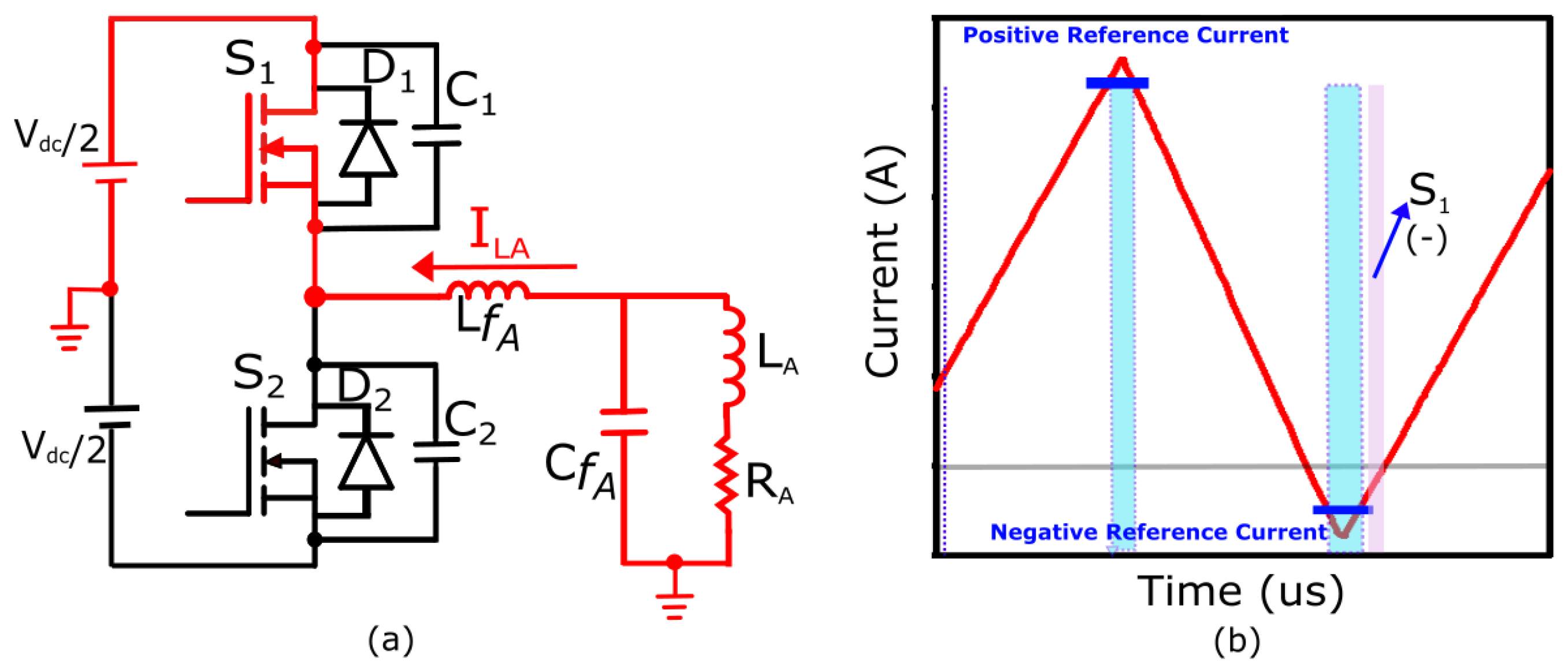
2. Soft-Switched Inverter

2.1. Circuit Topology

The diagram of a TCM-based ZVS two-level three-phase inverter with decoupled capacitors is shown in Figure 1. The inverter comprises components such as DC-link capacitors, SiC MOSFET switches with internal body diodes [37] and parasitic capacitance ( C d s ), an LC low-pass filter, and an RL load representing the Permanent Magnet Synchronous Motor (PMSM).
Two important aspects should be highlighted in the inverter topology.
  • Each switch is equipped with an external snubber capacitance ( C e x t ). The objective of this capacitance is to increase the overall capacitance across the switch. This increased capacitance plays an important role in achieving turn-off ZVS as outlined in [38]. The intentional presence of this enhanced capacitance serves to deliberately slow down the rise time of V d s during the turn-off transient, effectively reducing the overlap between non-zero V d s and I d s by distributing it over time.
  • The star point of the filter capacitors is connected to the mid-point of the dc-bus. This setup provides low-impedance pathways for high-frequency components within the inductor currents ( I L A , I L B , I L C ). Additionally, the wire connecting the dc-bus and filter capacitors serves as a pseudo fourth wire within the system, making it possible for the non-zero sum of the filter inductor currents to circulate back to the DC bus [39]. This connection helps in controlling the common-mode voltages of the filter capacitor. By managing the common-mode voltage in this manner, the EMI issues and leaking current [40] can be reduced. In motor-drive applications, this strategy can be employed to effectively reduce bearing currents [41,42]. It is noteworthy that harmonics could be introduced into this common mode [39], presenting an opportunity to lower both the required DC link voltage [43] and capacitance [44].

2.2. Principle of Operation

This research aims to achieve ZVS throughout the entire line cycle in a three-phase inverter by implementing the proposed AGDs. The output capacitance of the MOSFET and the role of the body diode are crucial in achieving turn-on ZVS through the incorporation of bidirectional inductor current. To comprehensively grasp the operation of the AGDs, a fundamental explanation of the single-phase half-bridge inverter is presented here.

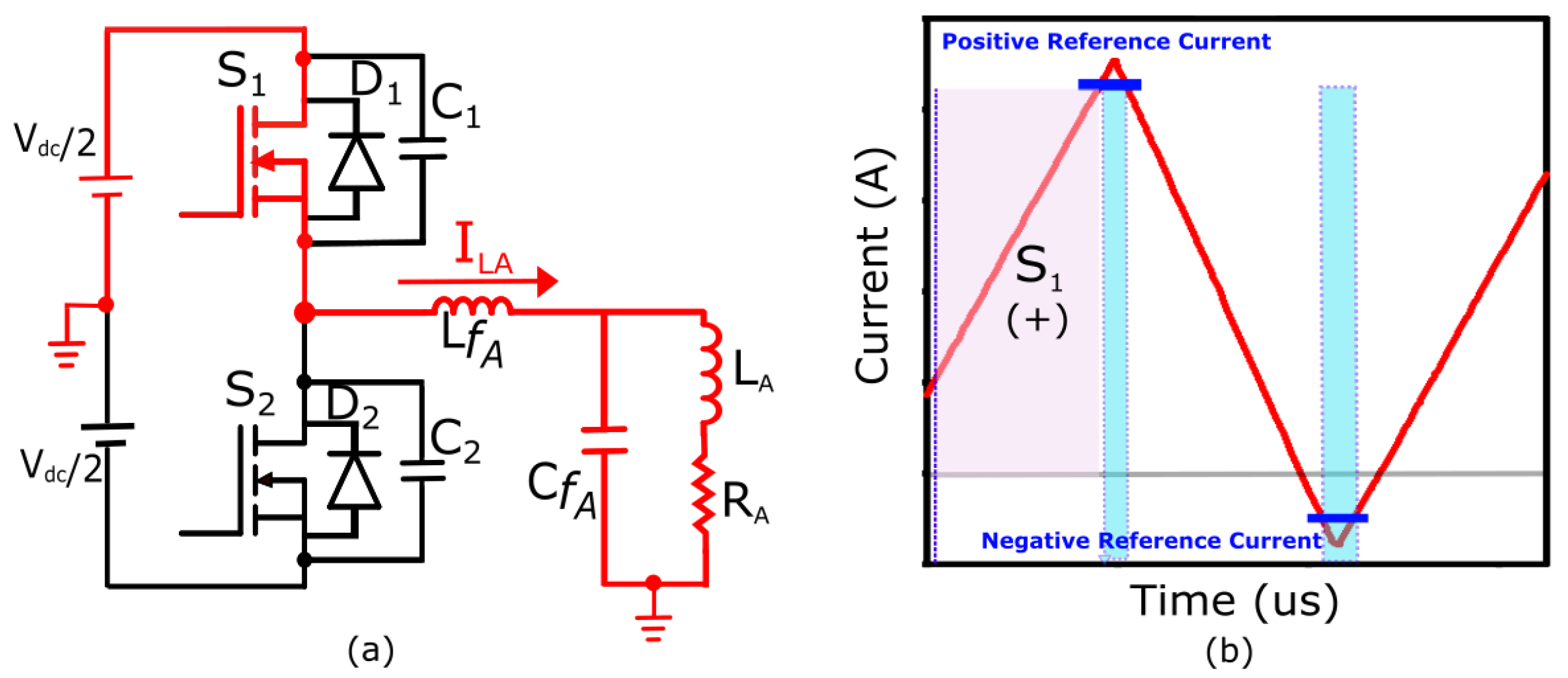
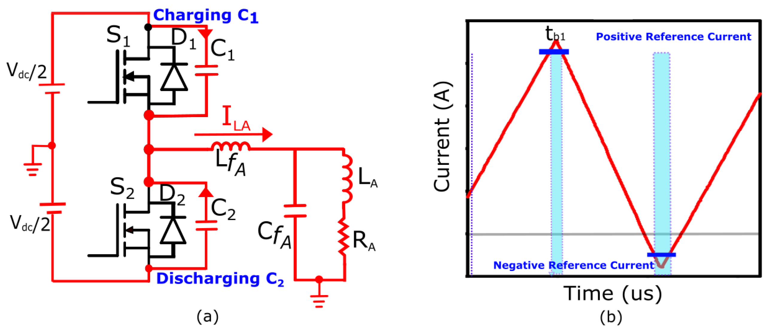
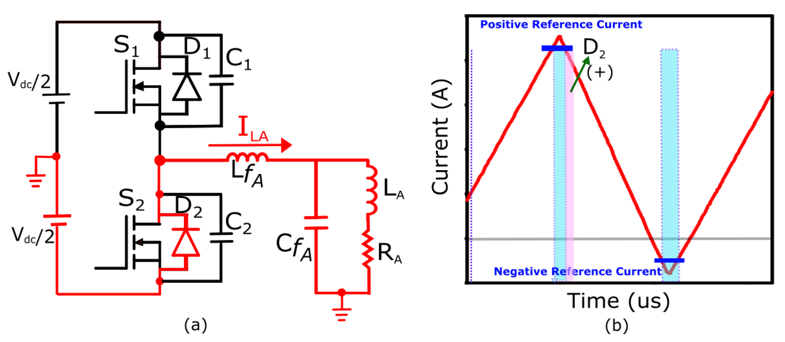
2.2.1. Operating Modes of a Single-Phase Half-Bridge Inverter
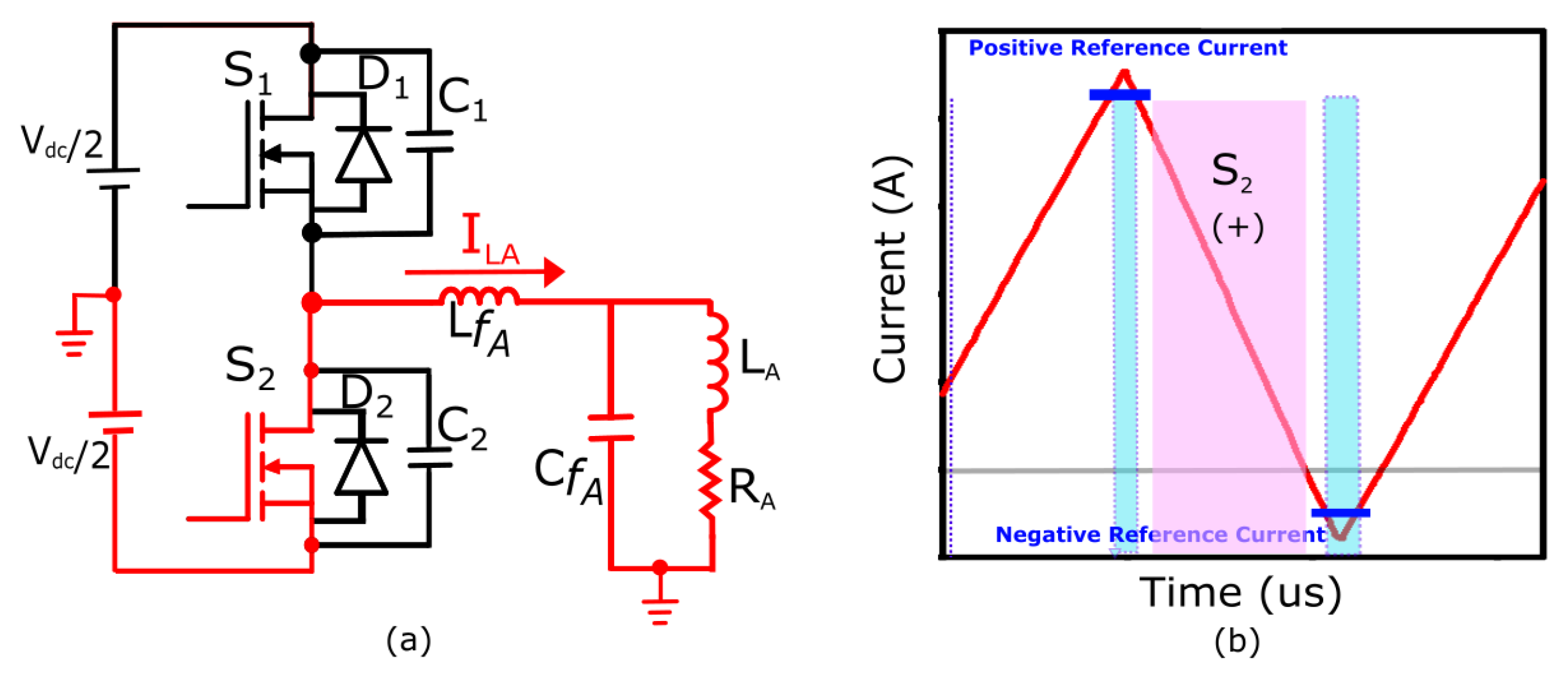
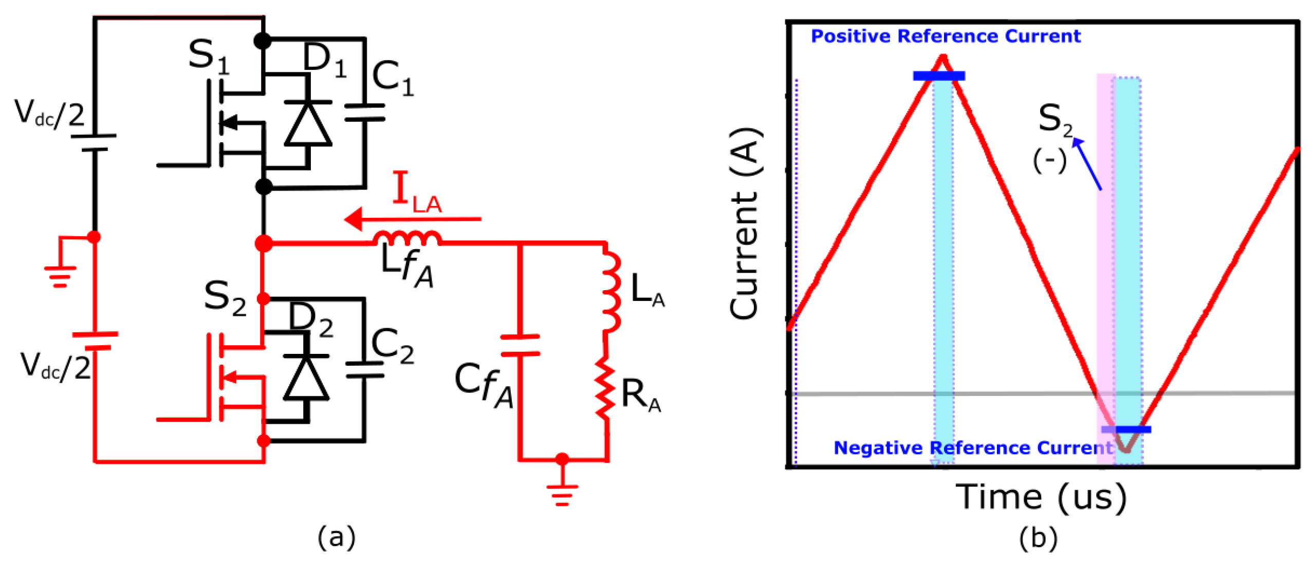
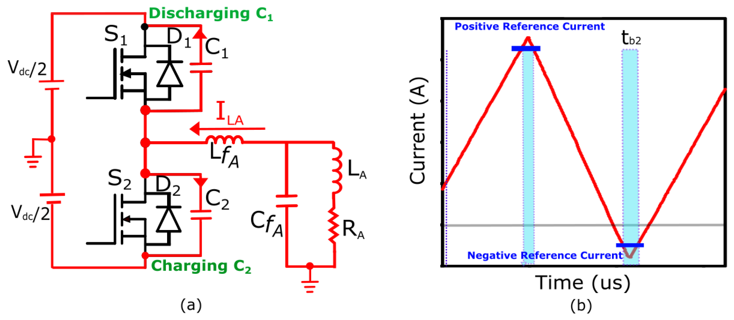
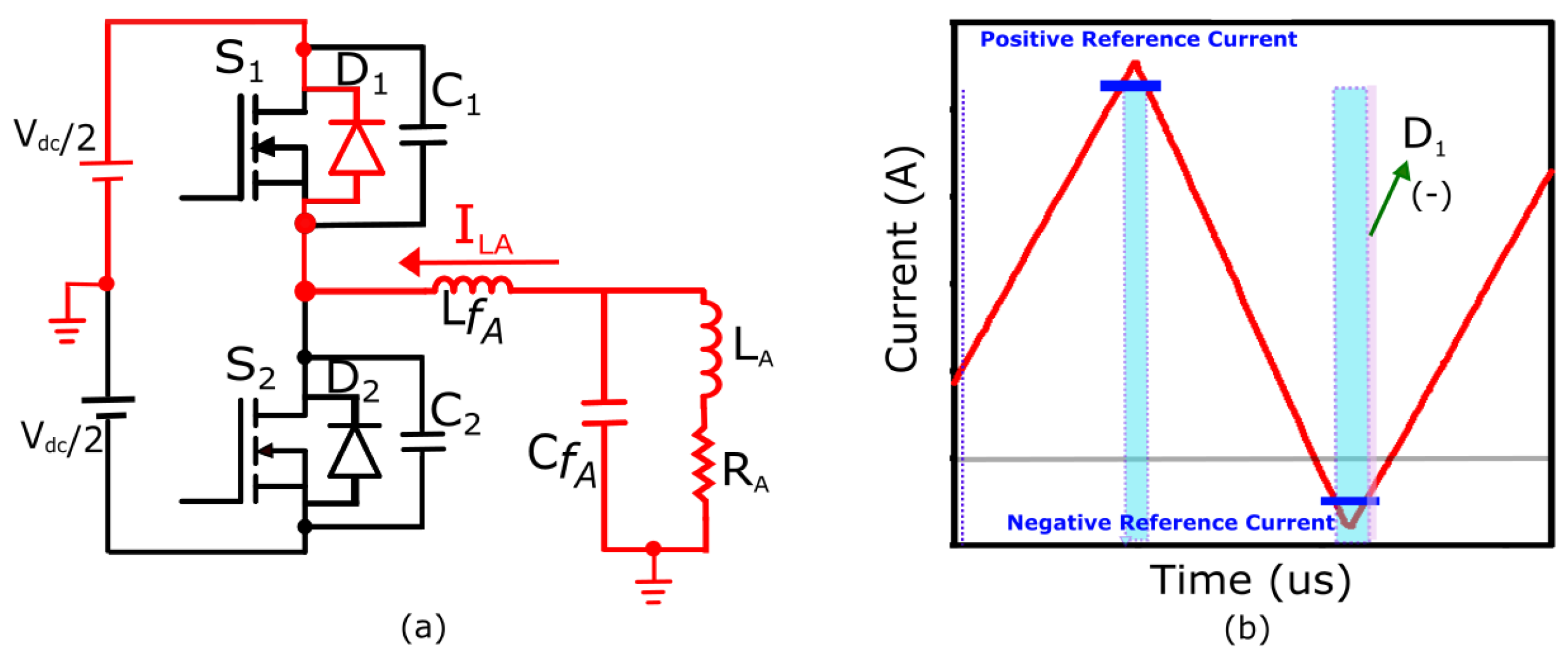
To understand the operating principle, each switching cycle of the inductor current is divided into eight distinct modes. These modes are determined by the direction of the inductor current and the conduction states of the associated switching devices, such as MOSFETs and body diodes.

Mode 1

This operational mode is initiated when the high-side switch S 1 is in the “on” state, while the low-side switch S 2 is in the “off” state. During this mode, the inductor current increases linearly due to the presence of positive voltage across it. Accordingly,
L f A d i A L ( t ) d t = V d c 2 V A N ( t ) ,
where L f A stands for inductance of phase A filter inductor, V d c is the dc-bus voltage and it is supposed that C i n 1 and C i n 2 are sufficiently large to keep the mid-point of the DC link constant, and V A N represents the voltage across the filter capacitor. Figure 2b illustrates one switching cycle of the inductor current, taking the form of a triangle andhence referred to as triangular-current mode. The shaded region in Figure 2b signifies the positive current flow through switch S 1 . The plus sign (+) shows the presence of a positive inductor current. In Figure 2a, the single-phase half-bridge inverter in phase A indicates that S 1 is conducting a positive current.

Mode 2

The high-side switch S 1 turns off when the current across the switch reaches the reference current value. At this moment, both switches are off and this period is known as blanking time-I denoted by ( t b 1 ) as shown in Figure 3b. During this interval, the magnitude of dv/dt remains nearly constant across both output capacitors. Subsequently, 1 2 I L is directed to charge the output capacitance of the S 1 switch to V d s 1 , while the other 1 2 I L discharges the output capacitance of the S 2 switch to zero voltage as shown in Figure 3a.

Mode 3

At the end of blanking time-I, the output capacitance of S 2 is completely discharged, resulting in a zero voltage across it. However, the voltage cannot be reduced further due to the presence of the body diode D 2 . Hence, the body diode D 2 initiates the conduction of a positive current as highlighted in Figure 4.

Mode 4

As the body diode D 2 conducts, the voltage across the low-side switch S 2 is zero. Under ZVS condition, the S 2 turns on, causing the inductor current, previously flowing through the body diode D 2 , to be transferred to the channel of the S 2 switch as shown in Figure 5.
Accordingly, during this phase, as the voltage across the inductor is negative, the inductor current undergoes a linear decrease.
L f A d i A L ( t ) d t = V d c 2 v A N ( t ) ,
where L f A stands for inductance of phase A filter inductor, V d c is the dc-bus voltage, and V A N represents the voltage across the filter capacitor.

Mode 5

This operational mode is triggered when the inductor current crosses zero and changes direction. Subsequently, S 2 begins to conduct a negative inductor current as illustrated in Figure 6. The minus sign (−) shows the presence of a negative inductor current.

Mode 6

For the ZVS turn-off of S 2 , the snubber capacitor plays a role here. The higher the snubber capacitance, the lower the overlap of V d s and I d s due to the increased charging time required by the snubber capacitance. S 2 turns off at ZVS. At this moment, both switches are turned off. This is the blanking time-II denoted by ( t b 2 ) as illustrated in Figure 7. During this period, the inductor current charges C 2 to V d s 2 and simultaneously discharges C 1 to zero voltage. The duration of this blanking interval is prolonged compared to blanking time-I, attributed to the presence of a relatively small inductor current.

Mode 7

Blanking time-II ends when C 2 is charged to C d s 2 and C 1 is discharged to zero voltage. Subsequently, the body diode D 1 of S 1 triggers the conduction of a negative inductor current as shown in Figure 8.

Mode 8

The operation of D 1 confirms the presence of zero voltage across S 1 , initiating ZVS for turn-on. Consequently, S 1 conducts a negative inductor current as depicted in Figure 9. With the reversal of the inductor current direction, S 1 transitions to conducting a positive inductor current, marking the completion of one switching cycle.

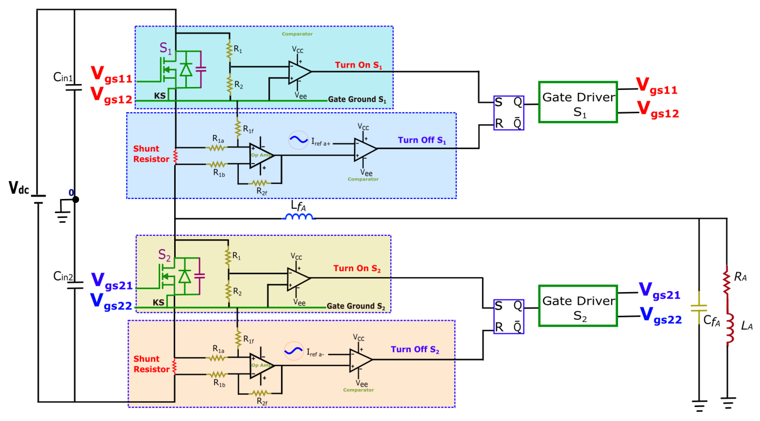
3. Autonomous Gate Drivers (AGDs)

The novelty of this work lies in the design of AGDs capable of achieving ZVS both at turn-on and turn-off of the switches with minimal time delay. The AGD generates the turn-on and turn-off signals for the switch while effectively controlling the peak output current at high speed.

3.1. Generation of Turn-on Signal

To achieve turn-on ZVS, the gate driver senses the drain-source voltage ( V d s ) across the switch. The AGD generates the turn-on signal for the switch when the voltage across it is slightly less than zero. This is accomplished using a high-speed comparator to check V d s , triggering the turn-on signal when V d s < 0. Here, it should be noted that the turn-on signal is under the control of the AGD. Therefore, duty cycle and frequency variations are governed by the AGD.

3.2. Generation of Turn-off Signal

Turning off the switch requires sensing the current across it by the gate driver. The AGD generates the turn-off signal when the switch current ( I d s ) exceeds the predefined reference current ( I r e f ). To achieve this, the switch current is sensed using a shunt resistor, as depicted in Figure 10. The voltage across the shunt resistor represents the current flow through the switch, and this voltage is amplified using a high-speed operational amplifier. The reference current is converted into a reference voltage for comparison with the amplified shunt voltage. A high-speed comparator is employed to compare the signals, generating the turn-off signal when I d s > I r e f . Achieving ZVS during turn-off involves utilizing the snubber capacitance.

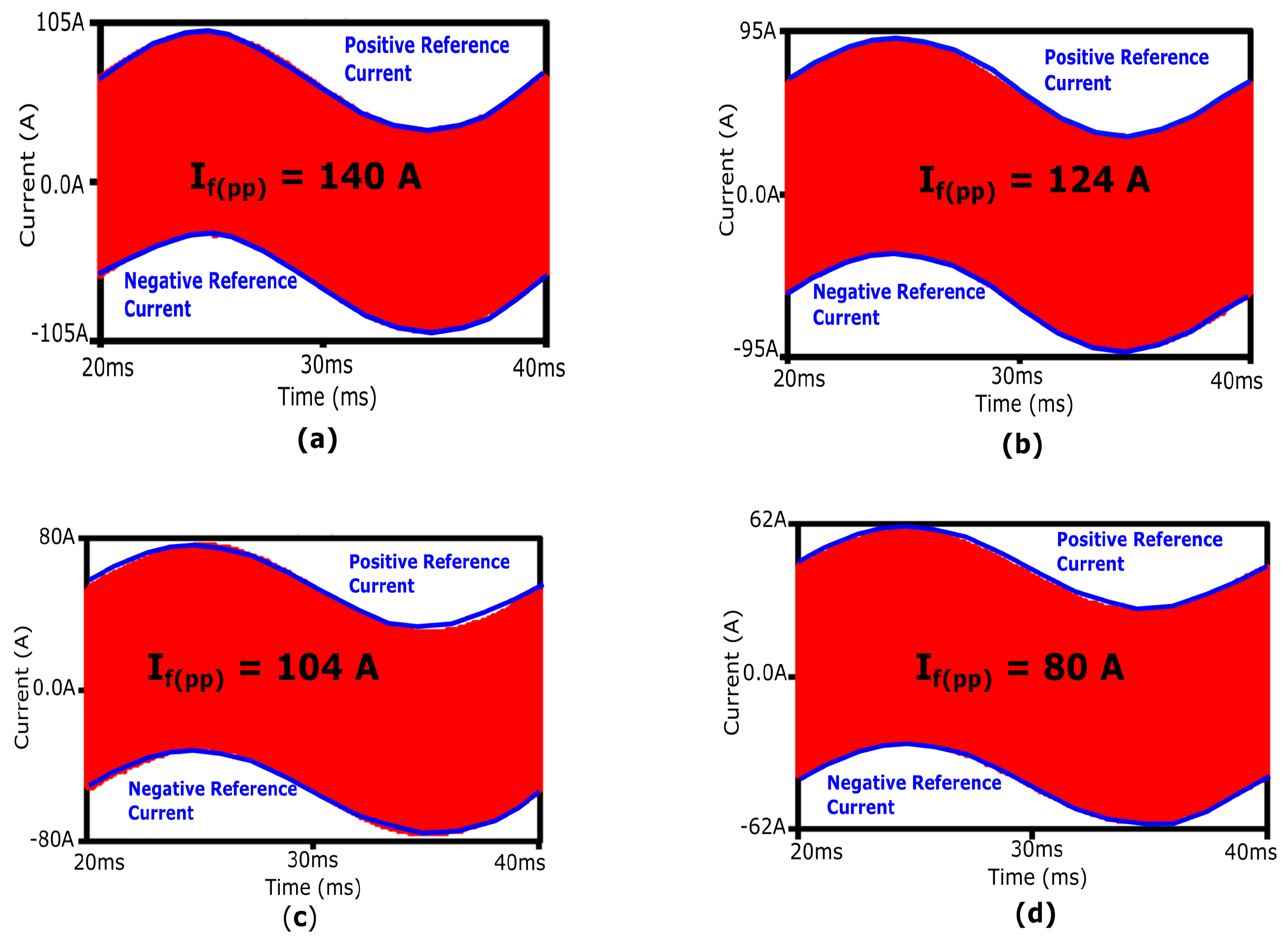
3.3. Generation of Reference Current

The motor control system uses a PMSM and aims to regulate the motor speed. The current control scheme is depicted in Figure 11. To achieve the required speed, the speed error between the measured and reference speeds is determined. A speed controller generates a reference torque ( T r e f ) based on the speed error. The reference torque is then converted into the quadrature component of the stator current ( I s q ) using a constant (k).
The inverse Park transformation converts the stator current components ( I s q , I d q ) back to a stationary reference frame ( I s α , I s β ). Subsequently, the inverse Clarke transformation converts the currents ( I s α , I s β ) from the stationary reference frame to the reference phase currents ( I a , I b , I c ). The reference current for each phase is then converted into a positive reference current for the high-side switch and a negative reference current for the low-side switch as shown in Figure 11.
The control scheme with the proposed AGDs is equally applicable to induction motors as well as to grid-connected inverters. This underscores the adaptability and relevance of the proposed strategy across diverse scenarios. However, the focus of this study has been on PMSM as it is relevant to electric vehicles.

4. Simulation Results and Discussion

4.1. Model Parameters

The inverter equipped with AGDs is designed to operate across various power levels, whether it is 10 kW, 100 kW, or 1 MW. For this study, a 10 kW power-rated inverter has been selected. The performance of the inverter is systematically assessed through simulations using LTspice XVII software, with a specific focus on the full-load operational mode within an electric vehicle drive system. Table 1 presents the electrical parameters of the proposed inverter utilized in the LTspice simulations.
In the real-world scenario, a PMSM is used. However, for simulation purposes, it has been substituted with an equivalent RL model, which is valid only under steady-state conditions. This RL load is integrated into the simulation model to provide a specific voltage. Table 2 outlines the electrical parameters of the PMSM, as employed in the LTspice simulations.

4.2. Operation of the Proposed AGD

The AGD senses the voltage across the switch. When the voltage is less than zero, the high-speed comparator generates the turn-on signal for the switch as illustrated in Figure 12a. The turn-on of the switch is under the control of the gate driver. Therefore, the AGD determines when to turn on the switch.
For turn-off, the switch current must exceed the reference current value. The comparator compares the signals and generates a turn-off signal for the switch, as depicted in Figure 12b. The turn-off of the switch is determined by the reference current.
The turn-on signal from voltage sensing and the turn-off signal from current sensing are then sent to the RS latch. The RS latch generates the V g s signal for the switch as shown in Figure 12c.

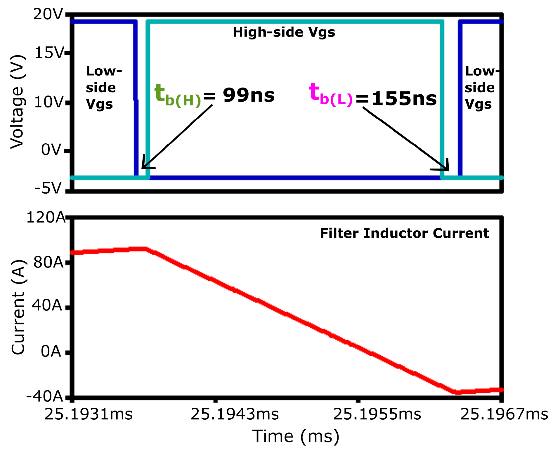
4.3. Impact of Inductor Current on Blanking Time

The AGD provides sufficient blanking time to both switches to prevent shoot-through. However, there is a variable optimum blanking time for each interval due to the sinusoidal line cycle. The AGD determines when to turn on the switch at ZVS.
The blanking time varies for different inductor current values. It is short for high positive or negative currents as it rapidly charges/discharges the output capacitance across the switch. Conversely, the blanking time is long for low positive or negative currents as it takes more time for the inductor current to charge/discharge the output capacitance [45], as depicted in Figure 13.

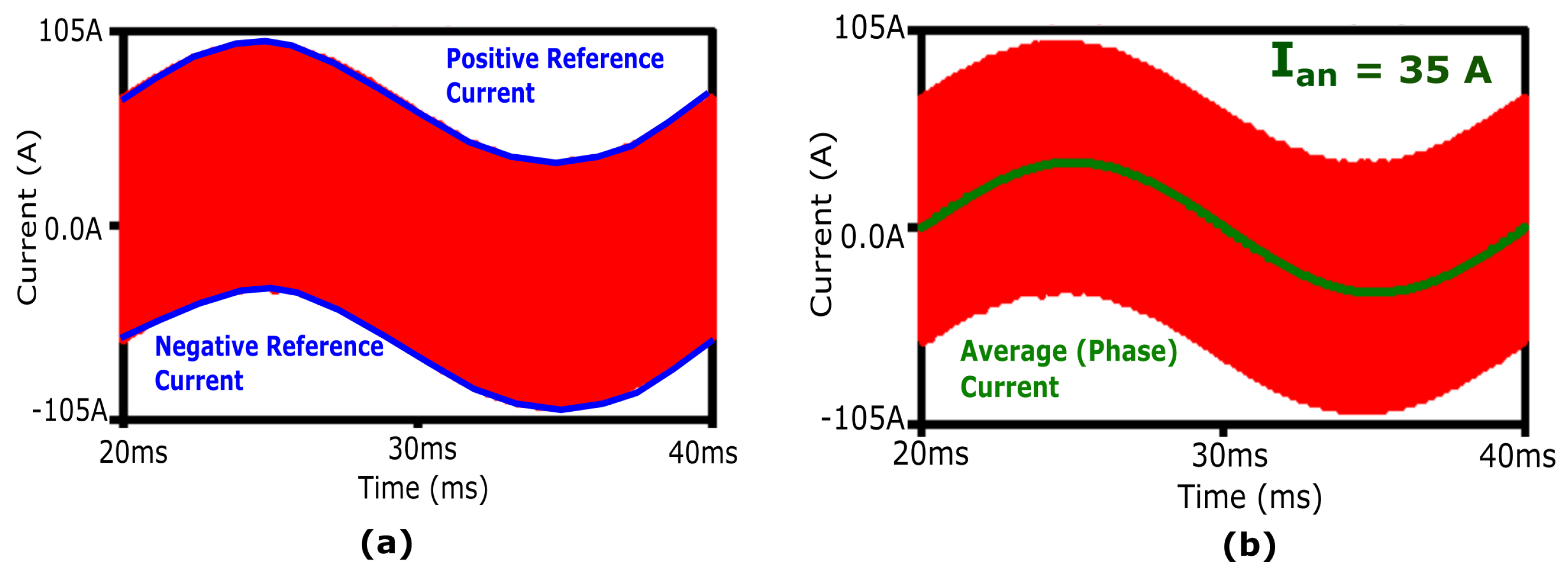
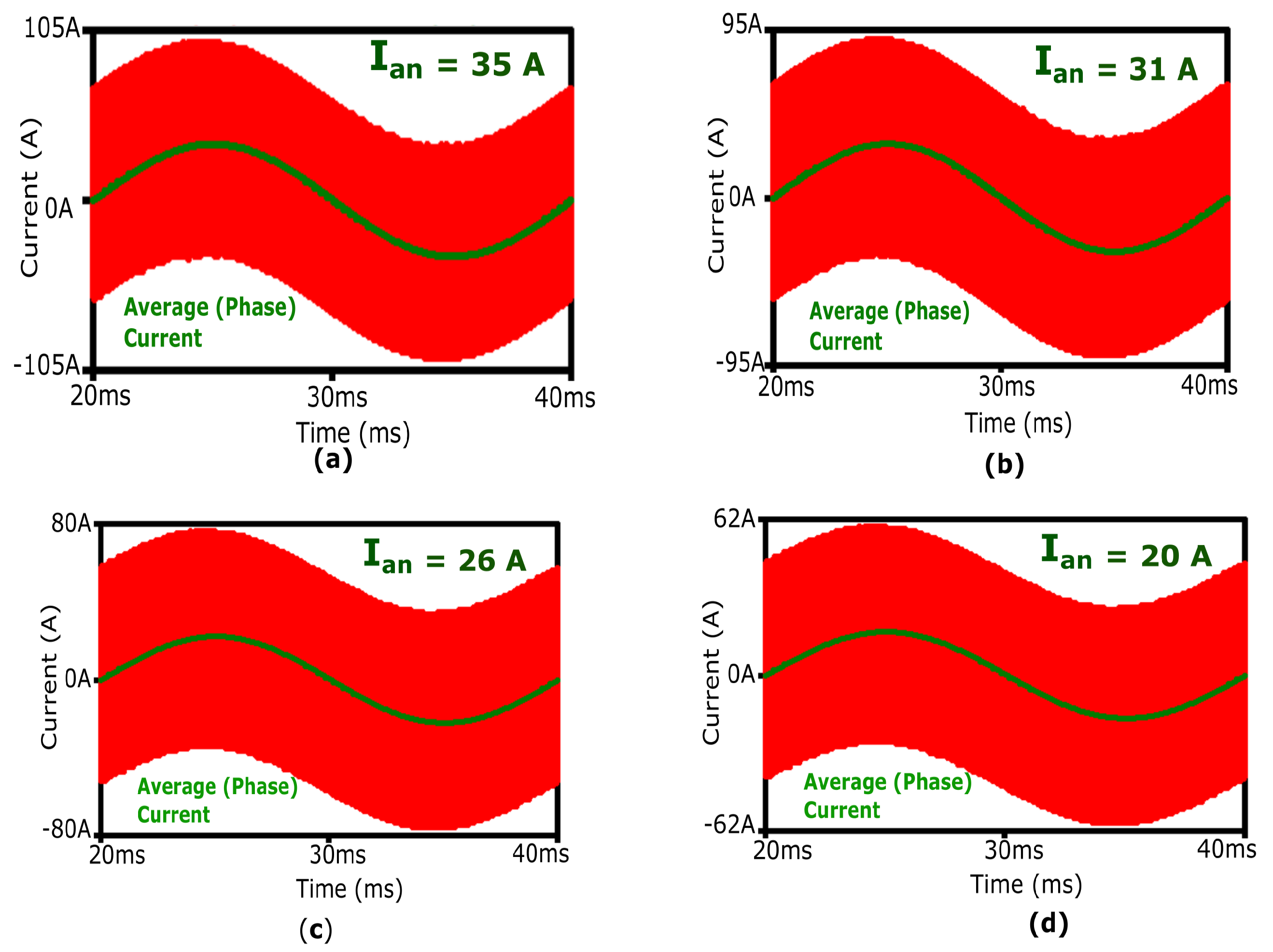
4.4. Reference Current and Inductor Current

To achieve the desired speed of the electric vehicle, the speed controller generates the reference currents. The reference current defines the upper and lower boundaries of the filter inductor current which enables ZVS with TCM/BCM [22,24] control. Depending on the configuration of these current limit boundaries, three distinct modulations of inductor current can be utilized to achieve ZVS operation: TCM/BCM with fixed reverse current, TCM/BCM with variable reverse current, and TCM/BCM with fixed bandwidth [28]. The proposed AGD can work efficiently with all three modes. For this study, the TCM with fixed bandwidth is taken into consideration.
The reference current values play a crucial role in determining the ripple in the inductor current. The peak-to-peak ripple of the inductor current consists of sinusoidal fundamental and high-frequency components as shown in Figure 14a. The sinusoidal component as phase current in Figure 14b primarily flows to the load, whereas the high-frequency part (the triangular portion) is predominantly directed towards the capacitors [39].
The ripple in the inductor current is calculated as [19]:
I L p p = K < I L avg > ,
where I L pp is the peak-to-peak ripple current, K is a constant, and I L a v g is the sinusoidal fundamental component of current.
From Figure 14, it can be seen that the output current is 35 A for full load, operating at a rated power of 10 kW with TCM fixed bandwidth. The required peak-to-peak current ripple is 140 A based on (3).

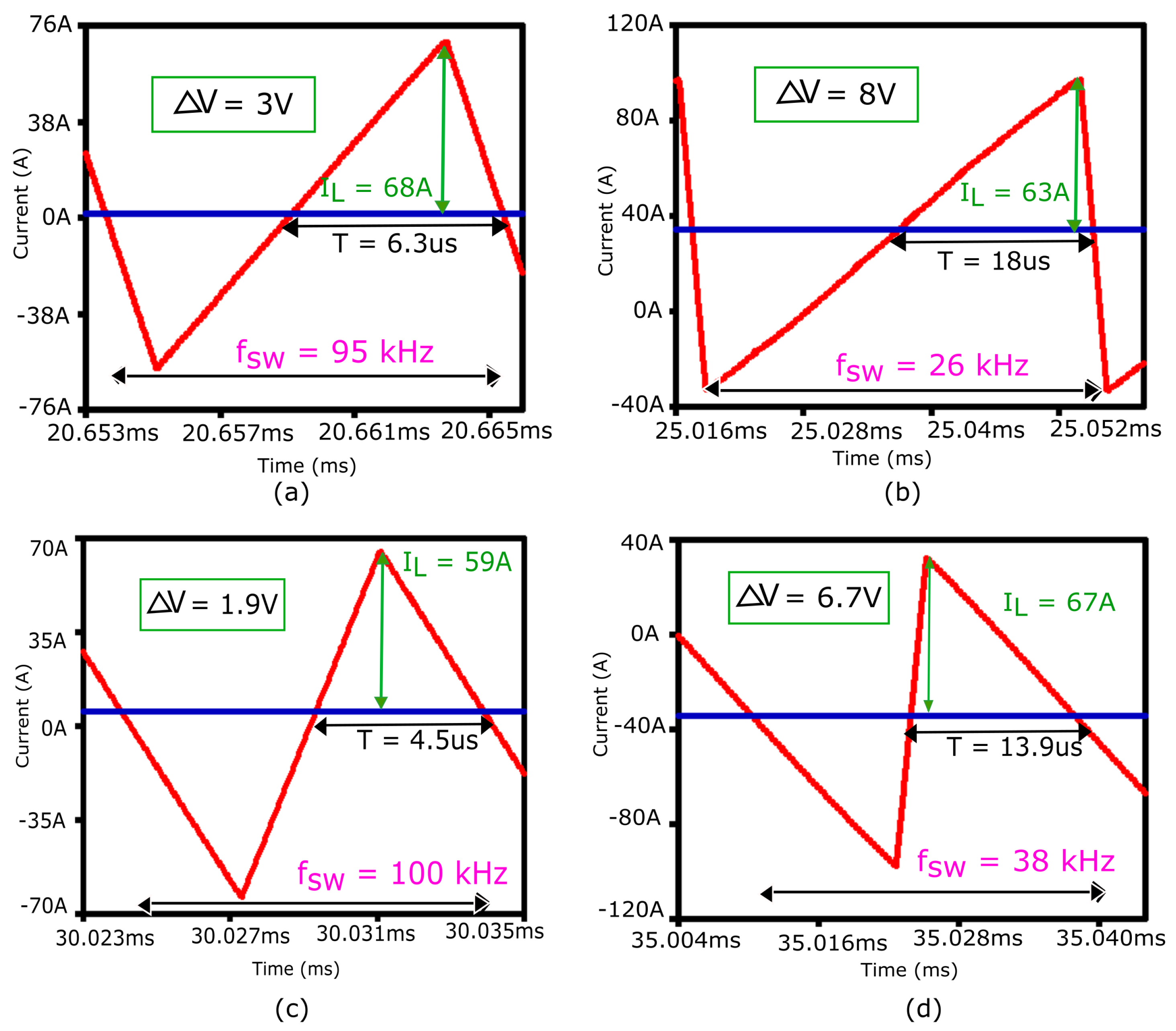
4.5. Effect of Variation in Switching Frequency on LC Filter

The switching frequency fluctuates throughout the fundamental line cycle, depending on the inductor current.
  • At the zero crossing point, the switching frequency is maximum [46].
  • At the peak of the fundamental line cycle, the switching frequency is minimum.
The variation in switching frequency at four different points in one fundamental line cycle is illustrated in Figure 15.
The different values of switching frequency are mentioned in Table 3.

4.5.1. Ripple in Inductor Current

The amplitude of the inductor ripple current is determined by the reference current of the AGD. The inductance of the inductor is calculated by the maximum peak-peak ripple in the inductor current at minimum and maximum switching frequencies.

4.5.2. Ripple in Filter Voltage

The filter capacitor is chosen in such a way that the average voltage ripple on the capacitor is less than 5% of the output voltage. The ripple in the capacitor voltage is due to the high-frequency components of the inductor current flowing to the capacitor. The ripples in the capacitor voltage are calculated for four different points in one line cycle such as two points at zero crossings (20 ms and 30 ms), one at a positive peak (25 ms), and one at a negative peak (35 ms), as shown in Figure 15.
  • The minimum voltage ripple is at a high switching frequency which is at the zero crossings. The reason for this is the short time available to charge/discharge the capacitor by the inductor current.
  • The maximum voltage ripple is at low switching and it is less than the desired voltage ripple.

4.6. LC Filter Power Losses

In high-power inverters, the most commonly used filtering configuration is the second-order LC filter. According to this topology, both the inductor and capacitor contribute to losses. However, in general, the losses attributed to the inductor are relatively larger than those incurred by the capacitor.

4.6.1. Filter Inductor Power Losses

The inductor losses can be divided into two parts: copper loss (winding loss) and iron loss (core loss).
  • The copper loss arises from the resistance of the winding and is determined as follows:
    P cu = R ac × I L ( rms ) 2 ,
    where R a c represents the AC resistance and I L ( r m s ) denotes the root mean square (rms) value of the inductor current.
  • Iron loss, resulting from fluctuations in the magnetic field within the core, is divided into hysteresis loss and eddy current loss. Both hysteresis and eddy current losses are present, complicating accurate calculations. The hysteresis loop changes over the fundamental cycle of current, while eddy currents vary accordingly. Moreover, eddy currents are partly dependent on hysteresis, further complicating the calculation of iron losses. Therefore, for precise estimation of losses, it is preferable to measure them at various operating conditions and construct a model based on these measurements.

4.6.2. Filter Capacitor Power Losses

Power losses in filter capacitors primarily stem from two sources: resistive losses due to the equivalent series resistance (ESR) and dielectric losses. These losses are influenced by factors such as the frequency of operation, voltage ripple, and the technology employed in the capacitor.
  • Resistive losses: These losses occur as a result of the internal resistance of the capacitor. When current flows through the capacitor, it encounters resistance, leading to power dissipation in the form of heat. The formula to calculate power dissipation due to ESR is:
    P esr = E S R × I L ( rms ) 2 ,
    where P esr is the power dissipated due to ESR, and I L ( rms ) is the root mean square inductor current flowing through the capacitor.
  • Dielectric losses: These losses occur due to the imperfect insulation properties of the dielectric material within the capacitor.

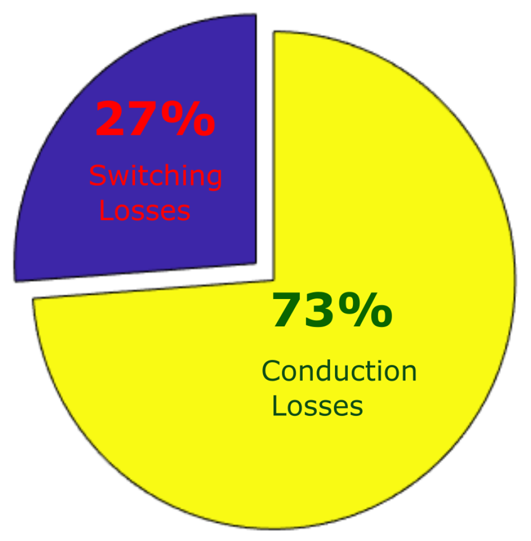
4.7. Power Losses in Inverter

Switching and conduction losses significantly contribute to determining the efficiency of a three-phase inverter, particularly in applications like motor drives.

4.7.1. Switching Losses
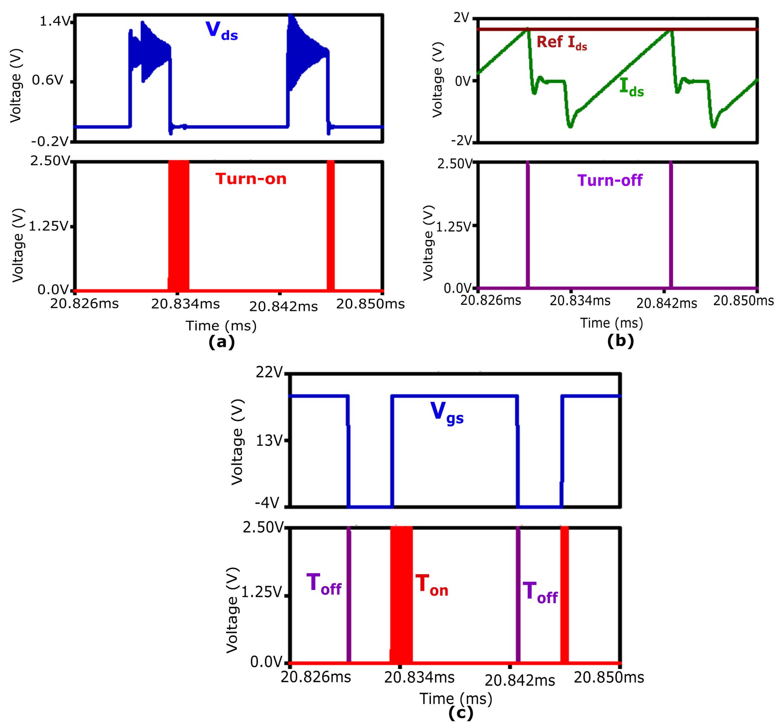
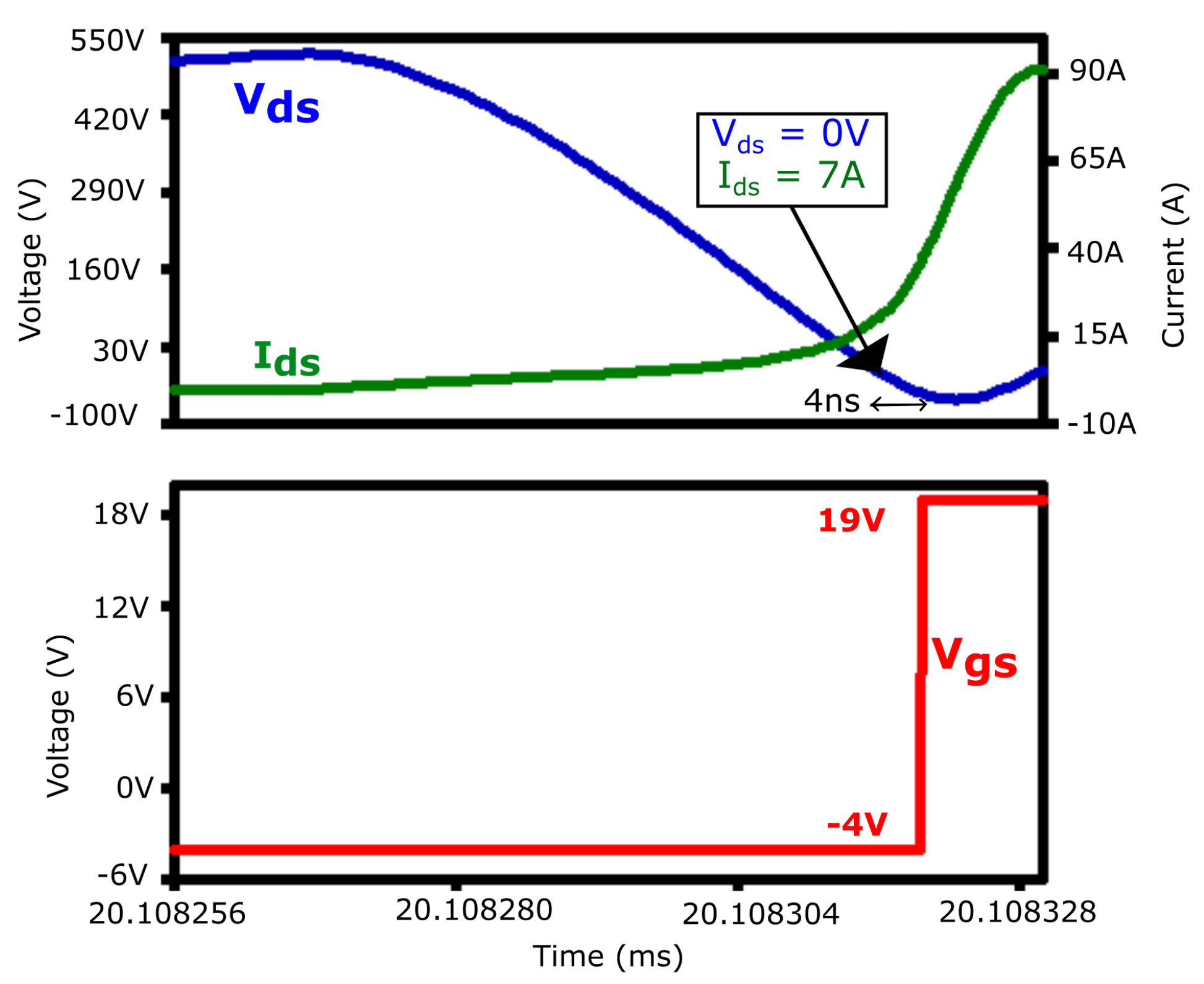
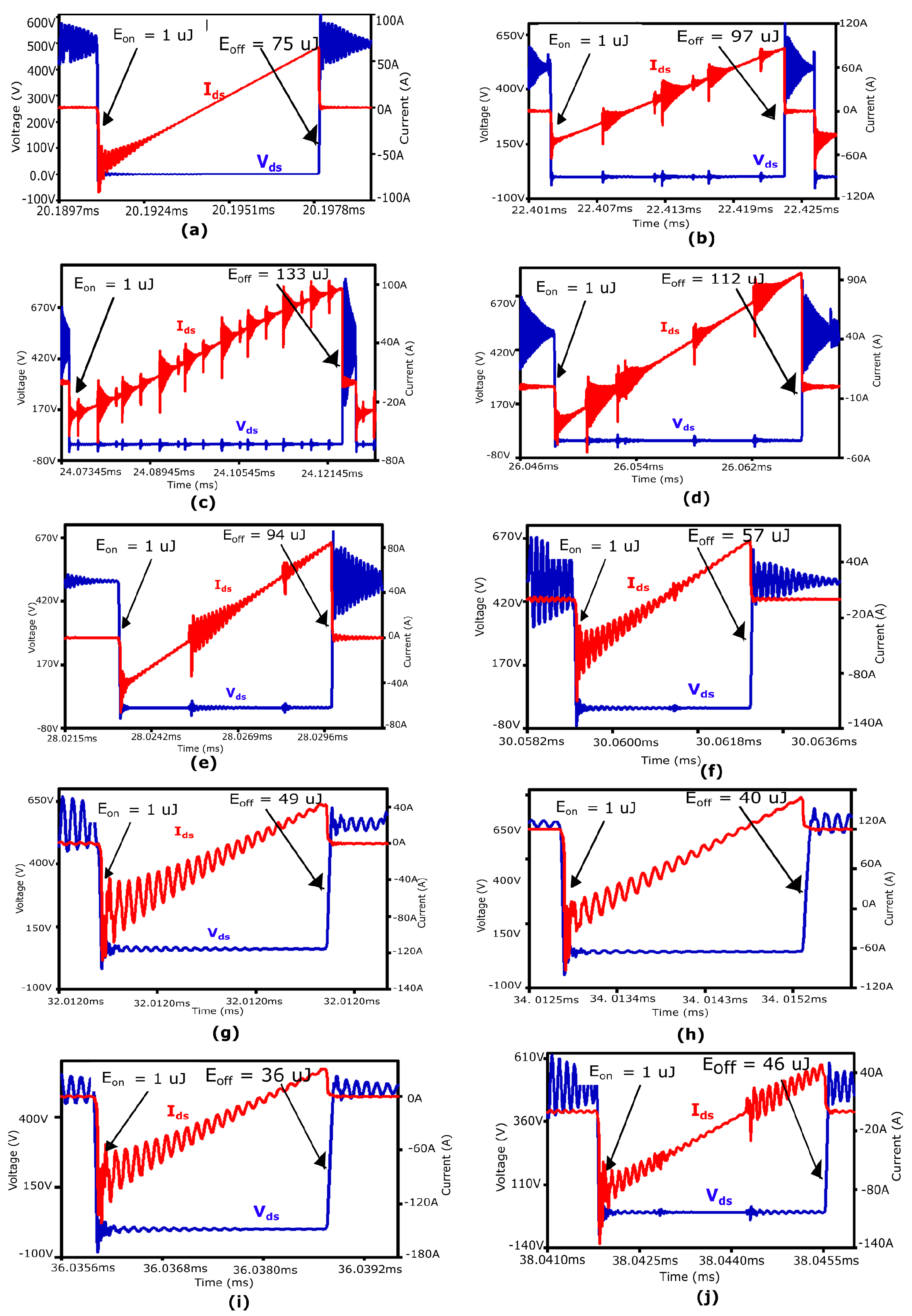
Switching losses in a MOSFET occur due to the overlap of the voltage V d s across the device and the current I d s passing through it during the turn-on and turn-off [47].
The expression for switching loss is given by the formula:
P sw = f sw × ( E on + E off ) × 6 ,
where E o n and E o f f represent the turn-on and turn-off energies of SiC MOSFET.
  • Turn-On Switching Losses
    In the proposed inverter, the turn-on switching losses are almost negligible due to the ZVS turn-on. Figure 16 illustrates that when the voltage across the switch is less than zero, the high-speed comparator of AGD detects it. After a delay of 4 nanoseconds, the AGD turns on the switch at zero voltage. Following the ZVS turn-on, the current starts flowing through the channel of the MOSFET.
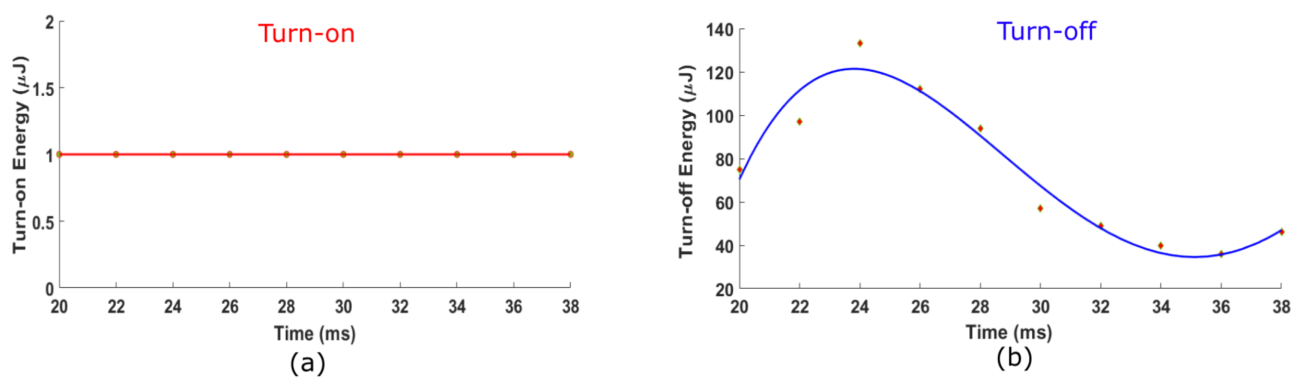
  • Turn-Off Switching Losses
Achieving turn-off ZVS can be accomplished by placing an appropriate snubber capacitance across the switch. However, there is no single snubber capacitance value that can consistently achieve ZVS turn-off due to the variations in the line current. Consequently, there are instances when turn-off switching losses are high.
A 10 kW power-rated inverter is examined in LTspice to calculate power losses. The power loss of the proposed inverter at a 10 kW power rating under steady-state conditions is determined to be 102 W, as calculated by LTspice software. Subsequently, a breakdown of the power loss (102 W) into switching and conduction losses is conducted.
To calculate the turn-on and turn-off switching losses after implementing the ZVS approach through the proposed AGDs, the one-line cycle (50 Hz, 20 ms) is subdivided into 10 points. All points are equally distributed throughout the entire cycle with a gap of 2 ms to obtain the best estimation of energy losses during each switching current as shown in Figure 17. These switching energies are calculated by LTspice simulation software.
Notably in Figure 17, the absence of high current peaks during switch turn-on and turn-off stages signifies a soft switching operation. Any oscillations observed while the switch is conducting are attributed to the turn-on of other switches in the remaining two legs, spaced at 120 and 240 degrees.
To better understand the behavior of switching energies, correlation-regression analysis was carried out for both turn-on and turn-off switching energies, as shown in Figure 18.
The correlation regression analysis shows that the turn-on energies do not depend on the amount of switch current due to the ZVS turn-on as illustrated in Figure 18a. However, the turn-off energies exhibit sinusoidal variation with the current as shown in Figure 18b. When the switch current is high in the positive cycle, the turn-off losses gradually increase with the switch current. At 25 ms, the switch current is maximum, resulting in higher turn-off energies. The same pattern is repeated for the negative cycle. However, the turn-off energies are comparatively lower in the negative half cycle due to the smaller amount of switch current.
After calculating the turn-off energies at 10 different points of one cycle, the average turn-off energy is taken into account, which is equal to 74 μ J, whereas turn-on energy is equal to 1 μ J.
  • The average switching energy for one switch is 75 μ J.
  • The average switching frequency for one line cycle = 64 kHz
The total switching losses in one line cycle can be calculated by (6) and it is equal to 29 W for 6 switches.

4.7.2. Conduction Losses

To attain ZVS during turn-on, a bidirectional inductor current is utilized. However, the inherent high ripples in the inductor current lead to elevated conduction losses, quantified by the formula:
P cd = 3 × ( I rms ) 2 × R DS ( on ) ,
where P c d represents the conduction power loss, and R D S ( o n ) depicts the on-state drain-source resistance of the SiC MOSFET channel. The value of switch current ( I rms ) has been calculated by LTspice software and is equal to 40 A. The total conduction losses in the proposed inverter are calculated by (7), and it is equal to 77 W for a 10 kW power-rated inverter.

4.7.3. Total Inverter Power Losses

The total power losses in the inverter calculated by LTspice are 102 W. The total power losses, manually calculated by individually determining the switching and conduction losses, amount to 106 W. The total power losses (switching and conduction losses) in the inverter are mentioned in Figure 19. The losses in the LC filter are not included in the power loss breakdown as the filter components were assumed to be lossless in the simulation model. However, in reality, losses in the filter inductor might be greater than the total losses in the inverter.
In Figure 19, it can be seen that switching losses account for 27% of the total losses, nearly equivalent to one-fourth of the total. However, conduction losses have increased significantly due to the high ripple in the inductor current.

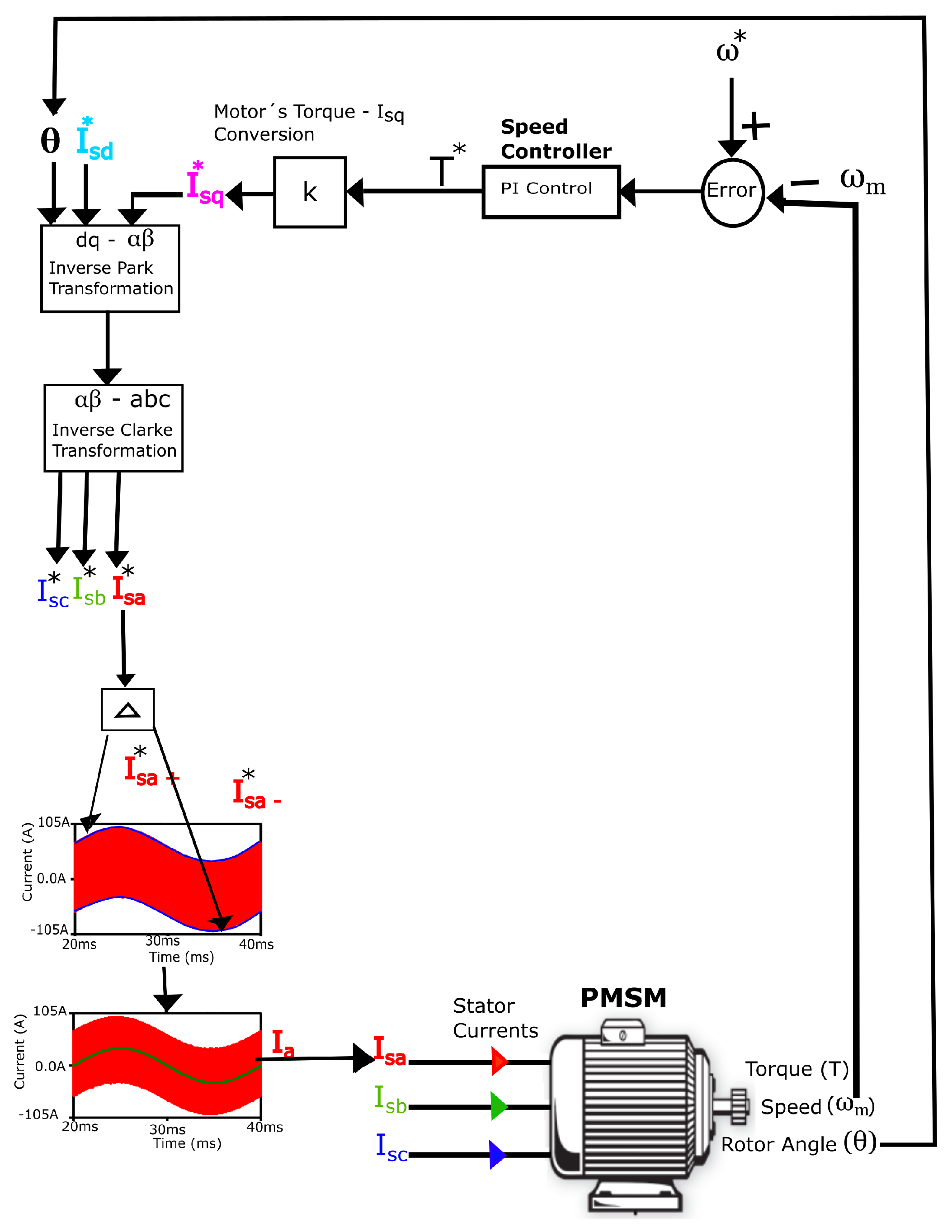
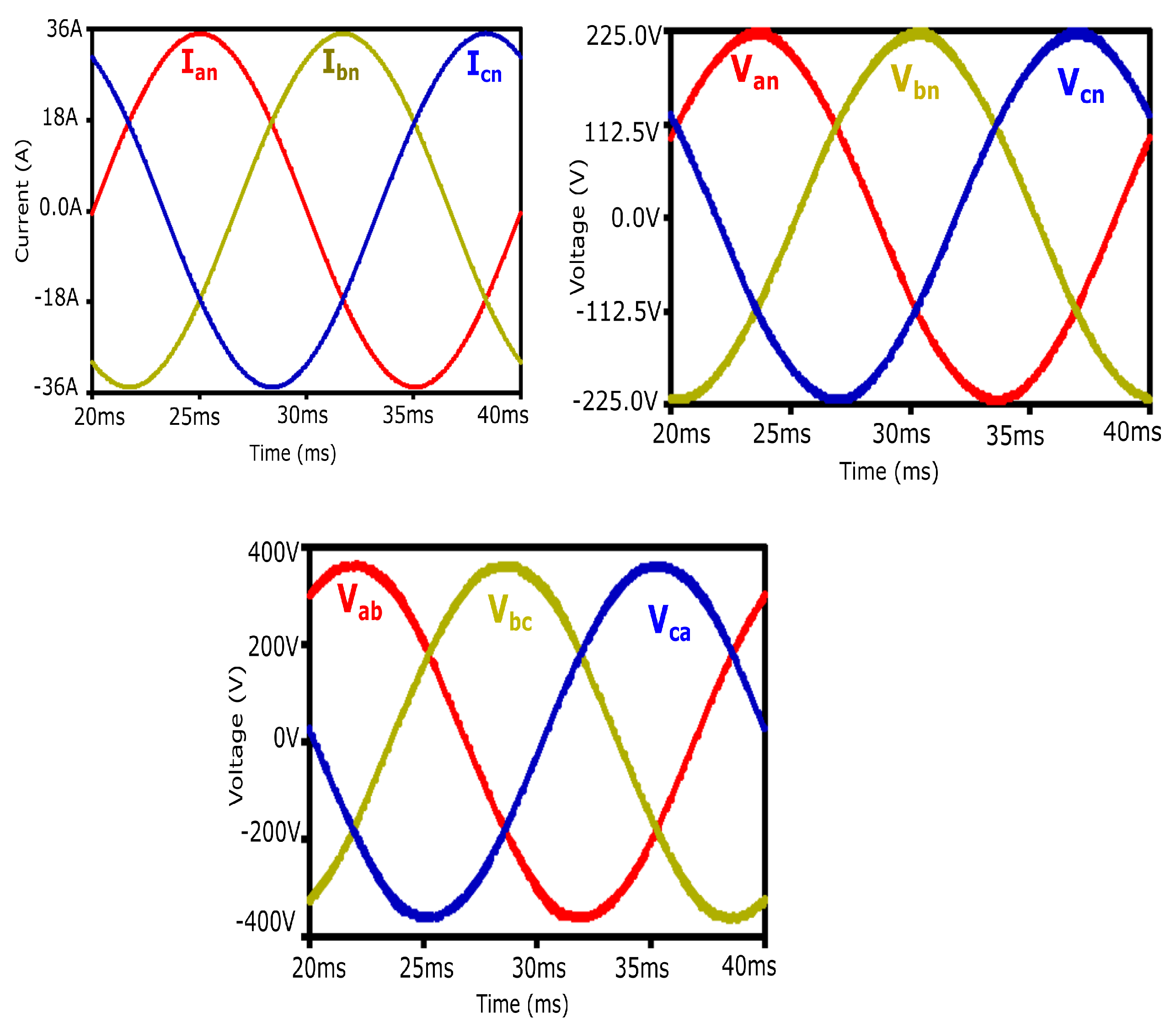
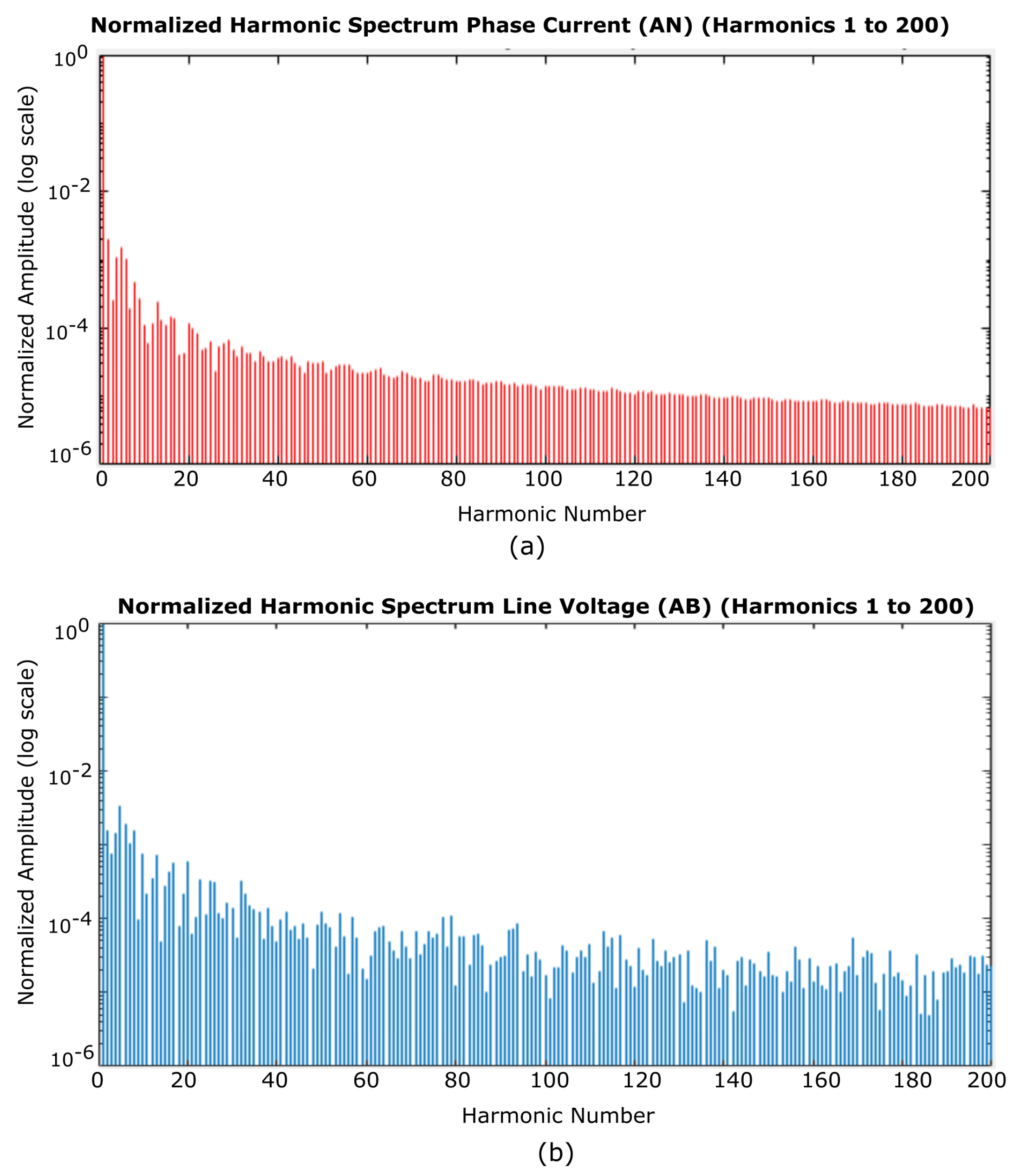
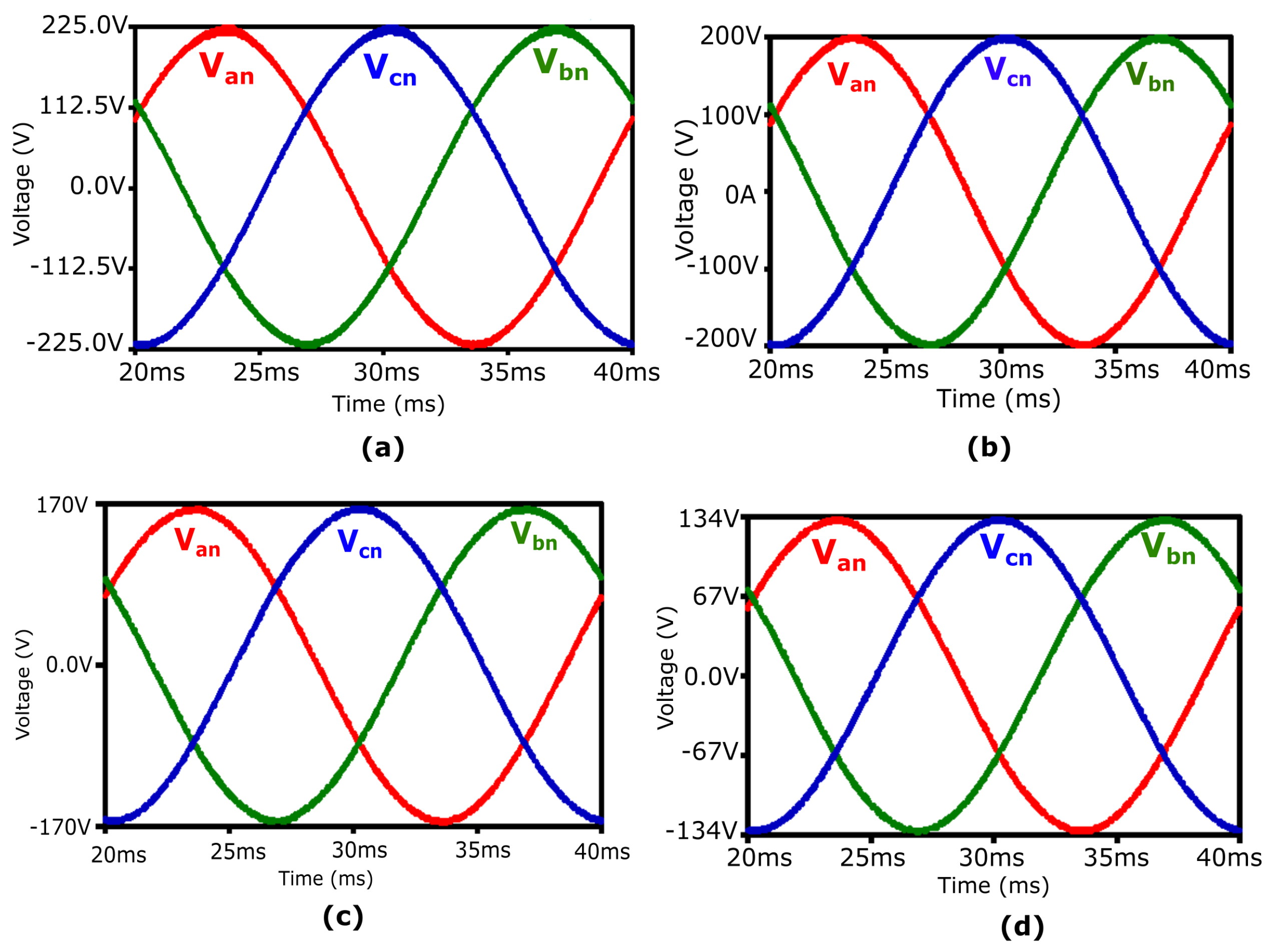
4.8. Sinusoidal Output Waveforms

One of the aims of this research work is to design ideal operating conditions for electric motor life. Sinusoidal output waveforms will preserve the motor windings and bearings, thereby enhancing the lifespan of the electric motor. With this goal in mind, the proposed inverter output waveforms are taken into consideration, as shown in Figure 20.
The observed current and voltage waveforms display sinusoidal characteristics. After observing these waveforms, the next step is to evaluate their quality. This is performed by analyzing their harmonic content. Harmonic spectra provide crucial insights into the presence and amplitudes of harmonic frequencies within the waveform. These harmonics, which are multiples of the fundamental frequency (typically the main frequency such as 50 Hz), can significantly impact the waveform’s characteristics.
To thoroughly assess the quality of the sinusoidal output waveforms, the harmonic spectra of both the phase current ( I an ) and the line voltage ( V a b ) are depicted in Figure 21.
In Figure 21a, the harmonic spectrum of the phase current shows minimized harmonic amplitudes, indicating a favorable waveform.
The harmonics in line voltage depend on the chosen filter capacitance value. A higher capacitance value results in lower harmonic components. However, choosing too high of a capacitance value should be avoided because it will increase the volume of the filter components in the inverter. Therefore, there is a trade-off between volume and harmonic content in the line voltage. The harmonic components have a significantly lower magnitude in the harmonic spectrum of the line voltage, as shown in Figure 21b. The harmonic spectrum up to the 200th harmonics is considered for ease of analysis. The amplitude of the harmonics is thousands of times smaller than the fundamental component of the line voltage. To further reduce the harmonic content, increasing the filter capacitance value is necessary.
To gain a comprehensive understanding of the impact of harmonic components on the sinusoidal waveforms, Total Harmonic Distortion (THD) values were calculated using LTspice software.
  • For phase current ( I an ), the THD is 0.3%.
  • For line voltage ( V ab ), the THD is 0.5%.
For a capacitance value of 80 μ F, the THD of the line voltage is 0.5%, which is much lower compared to the line voltage of a hard-switched three-phase inverter.
These findings indicate a significant reduction in harmonic distortions, which is essential for preserving system efficiency and reliability.

4.9. Adaptive Control Features of Proposed AGDs
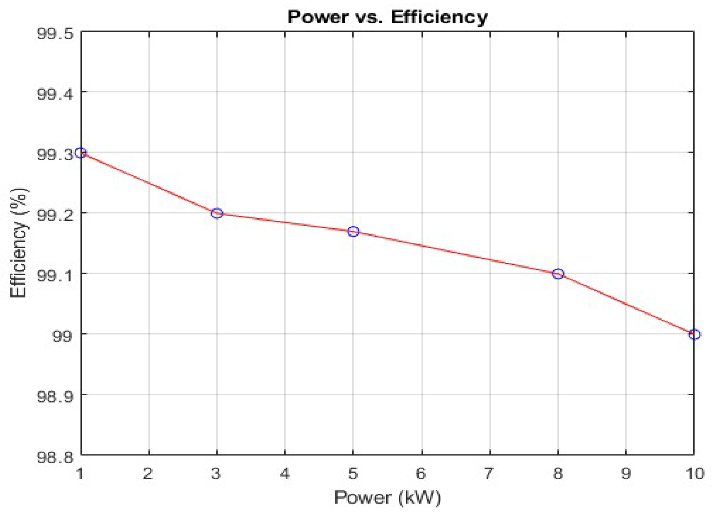
The AGD system demonstrates remarkable adaptability to varying conditions. By adjusting the reference current, the inductor ripples vary accordingly, as depicted in Figure 22. The output current is directly influenced by the inductor current ripple, where a higher ripple leads to higher average output currents, and vice versa, as shown in Figure 23. Robustness testing with four different reference currents confirms the AGD’s reliability. The adaptability of the proposed AGD is particularly advantageous in EVs, where low reference currents result in reduced inductor current ripple.
The phase voltages for four different reference currents are given in Figure 24.

4.10. Efficiency

To compute the efficiency of the inverter, LTspice software is employed to calculate both input and output powers. The input power of a three-phase inverter is derived as
P in ( avg ) = V d · I d ( avg ) .
Here, V d is assumed to be constant, and I d ( a v g ) represents the average value of the dc-link current.
The output power of a three-phase inverter is given by
P out ( avg ) = 1 T V a ( t ) I a ( t ) d t + V b ( t ) I b ( t ) d t + V c ( t ) I c ( t ) d t .
where V a , V b , and V c are the phase voltages of the load and I a , I b , and I c are the phase currents of the load.
The efficiency ( η ) of the inverter at steady-state conditions is calculated by
η = P out ( avg ) P in ( avg ) × 100 .
The power losses and efficiency for four different cases are mentioned in Table 4.
The efficiency plot over a wide range of the load power is presented in Figure 25.
It can be concluded from the variation of reference currents that:
  • By decreasing the reference value for the inductor current, the average value of the phase current decreases.
  • The efficiency increases with a low reference value. This is due to a reduction in conduction losses as the filter inductor ripple is small now. There is a probability of reduction in turn-off losses as the current ripple is small and there is less overlapping of voltage and current at turn-off.
Experimental results have shown that a hard-switched three-phase inverter may achieve an efficiency exceeding 99.5% [48]. Moreover, there is promising potential for the proposed soft-switching inverter to achieve efficiency surpassing 99% in the experimental setup. However, this relies on a well-designed filter inductor, a topic that is not within the scope of this paper.

4.11. EMI Mitigation

The proposed inverter offers a substantial reduction in both conductive and radiated EMI compared to a conventional two-level three-phase inverter, which represents a significant advantage.
Upon analyzing the output voltage and current waveforms, it is evident that conductive EMI is virtually absent due to the sinusoidal nature of these quantities. While the fundamental component remains the primary source of EMI, its magnitude is notably diminished compared to a standard two-level converter, owing to the negligible presence of harmonic components.
Similarly, radiated EMI is minimized, primarily originating from the fundamental component. Despite its unavoidable nature, the magnitude of radiated EMI is significantly reduced.

4.12. Hardware Design Recommendations

4.12.1. New Capacitor Technology: Enhanced Inverter Performance

The inverter with proposed AGDs emerges as a competitive technology for electric vehicles. If realized with new ceramic capacitor technologies [49], it might also be feasible to operate at comparably high temperatures. This facilitates the removal of the cooling system, allowing the inverter to be placed almost anywhere in the vehicle, preferably attached to the chassis. This will increase the power density of the inverter as well.

4.12.2. Impact of Increased Die Area on SiC MOSFET Performance and Losses

Increasing the die area of SiC MOSFETs leads to a rise in input and output capacitances, impacting turn-on, turn-off switching losses, and conduction losses. The effects can be broken down into several key points:
  • Input Capacitance Increase: By increasing the input capacitance, the turn-on losses will increase for hard-switched converters. This is due to the large oscillations produced by the LC loop involving the die input capacitance and inductance of the circuit. These oscillations will increase the EMI issues. To dampen these LC oscillations, the gate resistance needs to be increased. However, it will reduce the switching speed of the converter and increase the turn-on switching losses. But for soft-switched converters, this enhanced input capacitance will not affect the turn-on switching losses as the switch turns on at ZVS.
  • Output Capacitance Increase: By increasing the output capacitance, the turn-off losses will be reduced due to the less overlapping of V d s and I d s . Then there will be no need to use the external snubber capacitance as the elevated output capacitance will serve as snubber capacitance.
  • Die Area Increase: By increasing the die area, the resistance of the channel decreases and it will reduce the conduction losses. Another way to reduce the conduction losses is to use multiple parallel-connected MOSFETs that will reduce the R d s ( o n ) .
Figure 26 illustrates that increasing the die area of the MOSFET results in a dramatic reduction in conduction losses. However, in the case of a hard-switched converter, switching losses gradually increase. Conversely, for the proposed inverter, both conduction and switching losses decrease with increasing die area.
In summary, SiC MOSFETs with larger chip areas notably reduce conduction and turn-off losses. However, the impact on turn-on losses is negligible due to the ZVS technique. Another advantage of a larger die size is the enhancement of the cooling area, contributing to more effective thermal management.

4.12.3. Filter Inductor Design

In ZVS three-phase inverters, ferrite and Kool Mu cores are vital for filter inductor design:
  • Ferrite cores [50] (with litz and/or foil windings) suppress EMI and maintain high-frequency operation, ensuring clean power output.
  • Kool Mu cores [51] offer efficient energy storage with minimal losses, optimizing power conversion efficiency. Both cores enhance inverter performance and reliability.

4.12.4. Mitigating EMI in EVs: Shielding Considerations

Shielding is essential from the output of the inverter to the input of the filter to mitigate radiated EMI caused by large current ripples and voltage slopes. Employing a metallic screen is necessary to contain these ripples effectively. Furthermore, connections to filter inductors and capacitors must be shielded to prevent both currents and voltages from emitting EMI in the electric vehicle.

5. Conclusions

This research investigates the design and implementation of AGDs for TCM-based ZVS two-level three-phase inverters tailored specifically for EV drive systems. Utilizing LTspice simulation software, a thorough evaluation of a 10 kW power-rated inverter equipped with the proposed AGDs was conducted. The results demonstrate a consistent achievement of turn-on ZVS throughout the line cycle, with turn-off ZVS dependent on the snubber capacitance value. Notably, the inverter exhibited remarkable efficiency, exceeding 99%, making it highly suitable for EV applications. The observed sinusoidal output current and voltage waveforms, coupled with minimal harmonic distortions evidenced by low THD values, highlight the inverter’s effectiveness. Furthermore, the significant reduction in both conductive and radiated EMI compared to conventional inverters, attributed to the sinusoidal output waveforms, represents a notable advancement in EV drive system efficiency and reliability. This research represents a significant step forward in advancing sustainable transportation through the development of efficient and dependable EV propulsion technologies.

6. Future Work

Future research involves injecting the third-harmonic (zero-sequence) components into the three current references to enhance the modulation index of the inverter, consequently increasing the voltages at the filter capacitors. Given the significant losses associated with the filter inductor in this proposed design, comprehensive optimization of the ferrite core, incorporating techniques such as litz winding or foil winding, and the utilization of Kool Mu powder, will be conducted. Currently, the hardware design of the AGDs is in progress. The initial focus will be on validating the intended operation of the proposed AGDs within the experimental setup of the inverter. Upon successful validation, the inverter will undergo a series of comprehensive tests, which will include assessments against EMI standards as mandated by electric car manufacturing companies.

Author Contributions

Conceptualization, K.A. and H.-P.N.; methodology, K.A. and H.-P.N.; software, K.A.; validation, H.-P.N.; formal analysis, K.A.; Software, K.A.; investigation, K.A. and H.-P.N.; writing—original draft, K.A.; writing—review and editing, H.-P.N.; visualization, K.A.; supervision, H.-P.N.; project administration, K.A.; funding acquisition, H.-P.N. All authors have read and agreed to the published version of the manuscript.

Funding

This work has received funding from the Swedish Energy Agency.

Data Availability Statement

The data presented in this study are available upon request from the corresponding author. However, the data are not publicly available at this time due to ongoing extensions for further research purposes. For inquiries regarding the data, please contact the corresponding author.

Conflicts of Interest

The authors declare no conflicts of interest.

Abbreviations

The following abbreviations are used in this manuscript:
AGDsautonomous gate drivers
BCMboundary conduction mode
C d s drain-source capacitance
CMcommon mode
CCMcontinuous conduction mode
CRMcritical conduction mode
DCMdiscontinuous conduction mode
EMIelectromagnetic interference
ESRequivalent series resistance
EVselectric vehicles
IGBTsinsulated-gate bipolar transistors
MOSFETsmetal-oxide semiconductor field-effect transistors
PMSMPermanent Magnet Synchronous Motor
SiCsilicon carbide
SSWsoft switching
TCMtriangular-current mode
THDtotal harmonic distortion
V d s drain-source voltage
V g s gate-source voltage
ZCSzero-current switching
ZVSzero-voltage switching

References

  1. Nitta, N.; Wu, F.; Lee, J.T.; Yushin, G. Li-ion battery materials: Present and future. Mater. Today 2015, 18, 252–264. [Google Scholar] [CrossRef]
  2. Kong, L.; Wang, L.; Zhu, J.; Bian, J.; Xia, W.; Zhao, R.; Lin, H.; Zhao, Y. Configuring solid-state batteries to power electric vehicles: A deliberation on technology, chemistry and energy. Chem. Commun. 2021, 57, 12587–12594. [Google Scholar] [CrossRef]
  3. Jan, W.; Khan, A.D.; Iftikhar, F.J.; Ali, G. Recent advancements and challenges in deploying lithium-sulfur batteries as economical energy storage devices. J. Energy Storage 2023, 72, 108559. [Google Scholar] [CrossRef]
  4. Mazumder, H.; Ektesabi, M.; Kapoor, A. Effect of mass distribution on cornering dynamics of retrofitted EV. In Proceedings of the 2012 IEEE International Electric Vehicle Conference, Greenville, SC, USA, 4–8 March 2012; pp. 1–6. [Google Scholar] [CrossRef]
  5. Kretschmar, K.; Nee, H.-P. An AC Converter with a Small DC link Capacitor for a 15 kW Permanent Magnet Synchronous Integral Motor. In Proceedings of the International Conference on Power Electronics and Variable Speed Drives, London, UK, 21–23 September 1998; pp. 622–625. [Google Scholar] [CrossRef]
  6. Miric, S.; Niklaus, P.S.; Huber, J.; Stäger, C.; Haider, M.; Kolar, J.W. Analysis and Experimental Verification of the EMI Signature of Three-Phase Three-Level TCM Soft-Switching Converter Systems. IEEE Access 2023, 11, 57391–57400. [Google Scholar] [CrossRef]
  7. Ranstad, P.; Nee, H.-P. On Dynamic Effects Influencing IGBT Losses in Soft-Switching Converters. IEEE Trans. Power Electron. 2011, 26, 260–271. [Google Scholar] [CrossRef]
  8. Shirabe, K.; Swamy, M.; Kang, J.-K.; Hisatsune, M.; Wu, Y.; Kebort, D.; Honea, J. Advantages of high frequency PWM in AC motor drive applications. In Proceedings of the 2012 IEEE Energy Conversion Congress and Exposition (ECCE), Raleigh, NC, USA, 15–20 September 2012; pp. 2977–2984. [Google Scholar] [CrossRef]
  9. Nee, H.-P.; Kolar, J.W.; Friedrichs, P.; Rabkowski, J. Editorial: Special Issue on Wide Bandgap Power Devices and Their Applications. IEEE Trans. Power Electron. 2014, 29, 2153–2154. [Google Scholar] [CrossRef]
  10. Ranstad, P.; Nee, H.-P.; Linner, J.; Peftitsis, D. An Experimental Evaluation of SiC Switches in Soft-Switching Converters. IEEE Trans. Power Electron. 2014, 29, 2527–2538. [Google Scholar] [CrossRef]
  11. Zhang, L.; Yuan, X.; Wu, X.; Shi, C.; Zhang, J.; Zhang, Y. Performance evaluation of high-power SiC MOSFET modules in comparison to si IGBT modules. IEEE Trans. Power Electron. 2019, 34, 1181–1196. [Google Scholar] [CrossRef]
  12. Yan, Q.; Yuan, X.; Geng, Y.; Charalambous, A.; Wu, X. Performance evaluation of split output converters with SiC MOSFETs and SiC schottky diodes. IEEE Trans. Power Electron. 2017, 32, 406–422. [Google Scholar] [CrossRef]
  13. Haider, M.; Niklaus, P.S.; Madlener, M.; Rohner, G.; Kolar, J.W. Comparative Evaluation of Gate Driver and LC-Filter Based dv/dt-Limitation for SiC-Based Motor-Integrated Variable Speed Drive Inverters. IEEE Open J. Power Electron. 2023, 4, 450–462. [Google Scholar] [CrossRef]
  14. Jia, X.; Hu, C.; Dong, B.; He, F.; Wang, H.; Xu, D. Influence of system layout on CM EMI noise of SiC electric vehicle powertrains. CPSS Trans. Power Electron. Appl. 2021, 6, 298–309. [Google Scholar] [CrossRef]
  15. He, Y.; Zhu, J.; Zhou, B.; Zhao, X. EMI Issues and Reduction in 800 V Electrical Vehicle Systems by Incorporating Cable Effects. In Proceedings of the 2023 IEEE 6th Student Conference on Electric Machines and Systems (SCEMS), Huzhou, China, 7–9 December 2023; pp. 1–5. [Google Scholar] [CrossRef]
  16. Bosi, M.; Campanini, A.; Peretto, L.; Sanchez, A.M.; Pajares, F.J. Measurement equipment and optimal approach for power line filter design for automotive. In Proceedings of the 2022 IEEE International Workshop on Metrology for Automotive (MetroAutomotive), Modena, Italy, 4–6 July 2022; pp. 53–58. [Google Scholar] [CrossRef]
  17. Rao, H.; Zhou, B.; Zhang, F.; Xu, Y.; Hong, C.; Yang, J. Electromagnetic Compatibility of Power Electronic Devices in Electric Vehicle Drive System. In Proceedings of the 2021 IEEE 4th International Conference on Electronics Technology (ICET), Chengdu, China, 7–10 May 2021; pp. 509–512. [Google Scholar] [CrossRef]
  18. Xu, D.; Li, R.; He, N.; Deng, J.; Wu, Y. Soft-Switching Technology for Three-Phase Power Electronics Converters; Wiley: Hoboken, NJ, USA, 2021. [Google Scholar]
  19. Henze, C.; Martin, H.; Parsley, D. Zero-voltage switching in high frequency power converters using pulse width modulation. In Proceedings of the 3rd Annual IEEE Applied Power Electronics Conference and Exposition, New Orleans, LA, USA, 1–5 February 1988; pp. 33–40. [Google Scholar] [CrossRef]
  20. Xu, S.; Cao, B.; Chang, L.; Shao, R. Pulse Energy Modulation for a Single-Phase Bridge Inverter with Active Power Decoupling Capability. IEEE J. Emerg. Sel. Top. Power Electron. 2020, 9, 2014–2026. [Google Scholar] [CrossRef]
  21. Su, B.; Zhang, J.; Lu, Z. Totem-Pole Boost Bridgeless PFC Rectifier with Simple Zero-Current Detection and Full-Range ZVS Operating at the Boundary of DCM/CCM. IEEE Trans. Power Electron. 2011, 26, 427–435. [Google Scholar] [CrossRef]
  22. Cho, J.; Hu, D.; Cho, G. Three phase sine wave voltage source inverter using the soft switched resonant poles. In Proceedings of the 15th Annual Conference IEEE Industrial Electronics Society, Philadelphia, PA, USA, 6–10 November 1989; pp. 48–53. [Google Scholar] [CrossRef]
  23. Haryani, N.; Ohn, S.J.; Hu, J.; Rankin, P.; Burgos, R.; Boroyevich, D. A Novel ZVS Turn-on Triangular Current Mode Control with Phase Synchronization for Three Level Inverters. In Proceedings of the 2018 IEEE Energy Conversion Congress and Exposition (ECCE), Portland, OR, USA, 23–27 September 2018; pp. 2207–2214. [Google Scholar] [CrossRef]
  24. Cimendag, A.; Duman, T.; Yilmaz, M. 250W GaN Hybrid BCM Micro-inverter Design for Avionic Applications. In Proceedings of the 2022 IEEE Applied Power Electronics Conference and Exposition (APEC), Houston, TX, USA, 20–24 March 2022; pp. 838–842. [Google Scholar] [CrossRef]
  25. Marxgut, C.; Biela, J.; Kolar, J.W. Interleaved Triangular Current Mode (TCM) resonant transition single phase PFC rectifier with high efficiency and high power density. In Proceedings of the 2010 International Power Electronics Conference—ECCE Asia—IPEC, Sapporo, Japan, 21–24 June 2010; pp. 1725–1732. [Google Scholar] [CrossRef]
  26. Marxgut, C.; Krismer, F.; Bortis, D.; Kolar, J.W. Ultraflat Interleaved Triangular Current Mode (TCM) Single-Phase PFC Rectifier. IEEE Trans. Power Electron. 2014, 29, 873–882. [Google Scholar] [CrossRef]
  27. Haryani, N.; Sun, B.; Burgos, R. A novel soft switching ZVS sinusoidal input boundary current mode control of 6-switch three phase 2-level boost rectifier for active and active + reactive power generation. In Proceedings of the IEEE Applied Power Electronics Conference and Exposition (APEC), San Antonio, TX, USA, 4–8 March 2018; pp. 8–15. [Google Scholar] [CrossRef]
  28. Amirahmadi, A.; Hu, H.; Grishina, A.; Zhang, Q.; Chen, L.; Somani, U.; Batarseh, I. Hybrid ZVS BCM current controlled three-phase microinverter. IEEE Trans. Power Electron. 2014, 29, 2124–2134. [Google Scholar] [CrossRef]
  29. Chen, J.; Sha, D.; Zhang, J.; Liao, X. An SiC MOSFET based three-phase ZVS inverter employing variable switching frequency space vector PWM control. IEEE Trans. Power Electron. 2019, 34, 6320–6331. [Google Scholar] [CrossRef]
  30. Haryani, N.; Sun, B.; Burgos, R. ZVS turn-on triangular current mode (TCM) control for three phase 2-level inverters with reactive power control. In Proceedings of the IEEE Energy Conversion Congress and Exposition (ECCE), Portland, OR, USA, 23–27 September 2018; pp. 4940–4947. [Google Scholar] [CrossRef]
  31. Huang, Z.; Li, Q.; Lee, F.C. Digital-based soft-switching modulation for high-frequency three-phase inverters with reactive power transfer capability. In Proceedings of the IEEE Energy Conversion Congress and Exposition (ECCE), Portland, OR, USA, 23–27 September 2018; pp. 6751–6758. [Google Scholar] [CrossRef]
  32. Huang, Z.; Liu, Z.; Lee, F.C.; Li, Q. Critical-mode-based soft-switching modulation for high-frequency three-phase bidirectional AC–DC converters. IEEE Trans. Power Electron. 2019, 34, 3888–3898. [Google Scholar] [CrossRef]
  33. De Doncker, R.W.; Lyons, J. The auxiliary resonant commutated pole converter. In Proceedings of the Conference Record of the 1990 IEEE—Industry Applications Society Annual Meeting 1990, Seattle, WA, USA, 7–12 October 1990; Volume 2, pp. 1228–1235. [Google Scholar] [CrossRef]
  34. Haider, M.; Anderson, J.A.; Nain, N.; Zulauf, G.; Kolar, J.W.; Xu, D.M.; Deboy, G. Analytical Calculation of the Residual ZVS Losses of TCM-Operated Single-Phase PFC Rectifiers. IEEE Open J. Power Electron. 2021, 2, 250–264. [Google Scholar] [CrossRef]
  35. Anderson, J.A.; Zulauf, G.; Kolar, J.W.; Deboy, G. New Figure-of-Merit Combining Semiconductor and Multi-Level Converter Properties. IEEE Open J. Power Electron. 2020, 1, 322–338. [Google Scholar] [CrossRef]
  36. Zhang, D.; Zhang, Q.; Hu, H.; Grishina, A.; Shen, J.; Batarseh, I. High efficiency current mode control for three-phase micro-inverters. In Proceedings of the 2012 Twenty-Seventh Annual IEEE Applied Power Electronics Conference and Exposition (APEC), Orlando, FL, USA, 5–9 February 2012; pp. 892–897. [Google Scholar] [CrossRef]
  37. Sadik, D.-P.; Heinig, S.; Jacobs, K.; Johannesson, D.; Lim, J.-K.; Nawaz, M.; Dijkhuizen, F.; Bakowski, M.; Norrga, S.; Nee, H.-P. Investigation of the surge current capability of the body diode of SiC MOSFETs for HVDC applications. In Proceedings of the 2016 18th European Conference on Power Electronics and Applications (EPE’16 ECCE Europe), Karlsruhe, Germany, 5–9 September 2016; pp. 1–10. [Google Scholar]
  38. Agrawal, B.; Preindl, M.; Emadi, A. Turn-off energy minimization for soft-switching power converters with wide bandgap devices. In Proceedings of the 2017 IEEE International Conference on Industrial Technology (ICIT), Toronto, ON, Canada, 22–25 March 2017; pp. 236–241. [Google Scholar] [CrossRef]
  39. Wang, Q.; Burgos, R. A Method for Increasing Modulation Index of Three Phase Triangular Conduction Mode Converter. In Proceedings of the 2018 IEEE 19th Workshop on Control and Modeling for Power Electronics (COMPEL), Padua, Italy, 25–28 June 2018; pp. 1–5. [Google Scholar] [CrossRef]
  40. Serban, I. Power Decoupling Method for Single-Phase H-Bridge Inverters with No Additional Power Electronics. IEEE Trans. Ind. Electron. 2015, 62, 4805–4813. [Google Scholar] [CrossRef]
  41. Eull, M.; Preindl, M. A Soft Switching Inverter Minimizing Bearing Currents in 800V Electric Vehicle Drives. In Proceedings of the 2021 IEEE 13th International Symposium on Diagnostics for Electrical Machines, Power Electronics and Drives (SDEMPED), Dallas, TX, USA, 22–25 August 2021; pp. 457–463. [Google Scholar] [CrossRef]
  42. Eull, M.; Zhou, L.; Jahnes, M.; Preindl, M. Bidirectional Nonisolated Fast Charger Integrated in the Electric Vehicle Traction Drivetrain. IEEE Trans. Transp. Electrif. 2022, 8, 180–195. [Google Scholar] [CrossRef]
  43. Zhou, L.; Eull, M.; Wang, W.; Preindl, M. Modular Model-Predictive Control with Regulated Third-Harmonic Injection for Zero-Sequence Stabilized Inverter. IEEE Trans. Ind. Appl. 2022, 58, 7634–7647. [Google Scholar] [CrossRef]
  44. Tang, Y.; Yao, W.; Loh, P.C.; Blaabjerg, F. Highly Reliable Transformerless Photovoltaic Inverters with Leakage Current and Pulsating Power Elimination. IEEE Trans. Ind. Electron. 2016, 63, 1016–1026. [Google Scholar] [CrossRef]
  45. Abbas, K.; Nee, H.-P.; Kostov, K. Autonomously Modulating Gate Drivers for Triangular-Current Mode (TCM) Zero-Voltage Switching (ZVS) Buck Converter. In Proceedings of the 2023 22nd International Symposium on Power Electronics (Ee), Novi Sad, Serbia, 25–28 October 2023; pp. 1–6. [Google Scholar] [CrossRef]
  46. Fan, B.; Wang, Q.; Burgos, R.; Ismail, A.; Boroyevich, D. Adaptive hysteresis current based ZVS modulation and voltage gain compensation for high-frequency three-phase converters. IEEE Trans. Power Electron. 2021, 36, 1143–1156. [Google Scholar] [CrossRef]
  47. Mohan, N.; Undeland, T.M.; Robbins, W.P. Power Electronics: Converters, Applications, and Design; John Wiley & Sons: Hoboken, NJ, USA, 2003. [Google Scholar]
  48. Rabkowski, J.; Peftitsis, D.; Nee, H.-P. Design Steps Toward a 40-kVA SiC JFET Inverter with Natural-Convection Cooling and an Efficiency Exceeding 99.5%. IEEE Trans. Ind. Appl. 2013, 49, 1589–1598. [Google Scholar] [CrossRef]
  49. Neumayr, D.; Bortis, D.; Kolar, J.W.; Koini, M.; Konrad, J. Comprehensive Large-Signal Performance Analysis of Ceramic Capacitors for Power Pulsation Buffers. In Proceedings of the 17th IEEE Workshop on Control and Modeling of Power Electronics (COMPEL), Trondheim, Norway, 27–30 June 2016. [Google Scholar] [CrossRef]
  50. Burkart, R.M.; Uemura, H.; Kolar, J.W. Optimal inductor design for 3-phase voltage-source PWM converters considering different magnetic materials and a wide switching frequency range. In Proceedings of the 2014 International Power Electronics Conference (IPEC-Hiroshima 2014—ECCE ASIA), Hiroshima, Japan, 18–21 May 2014; pp. 891–898. [Google Scholar] [CrossRef]
  51. Nielsen, A.B.; Davari, P.; Blaabjerg, F.; Nielsen, B.V. Power Density and Loss Optimization Design Methodology of a 10 kW 2-Level 3-Phase SiC Inverter. In Proceedings of the 2020 IEEE 21st Workshop on Control and Modeling for Power Electronics (COMPEL), Aalborg, Denmark, 9–12 November 2020; pp. 1–7. [Google Scholar] [CrossRef]
Figure 1. Schematic representation of the proposed inverter.
Energies 17 01060 g001
Figure 2. Switch ( S 1 ) is conducting a positive current. (a) Positive current direction in a single-phase half-bridge inverter. (b) Highlighted switch current direction in the TCM of the filter inductor.
Energies 17 01060 g002
Figure 3. Blanking time-I. (a) Current directions during charging of C 1 and discharging of C 2 in a single-phase half-bridge inverter. (b) Highlighted blanking time ( t b 1 ) in the TCM of the filter inductor.
Energies 17 01060 g003
Figure 4. Body diode ( D 2 ) is conducting a positive current. (a) Positive current direction in a single-phase half-bridge inverter. (b) Highlighted diode current direction in the TCM of the filter inductor.
Energies 17 01060 g004
Figure 5. Switch ( S 2 ) is conducting a positive current. (a) Positive current direction in a single-phase half-bridge inverter. (b) Highlighted switch current direction in the TCM of the filter inductor.
Energies 17 01060 g005
Figure 6. Switch ( S 2 ) is conducting a negative current. (a) Negative current direction in a single-phase half-bridge inverter. (b) Highlighted switch current direction in the TCM of the filter inductor.
Energies 17 01060 g006
Figure 7. Blanking time-II. (a) Current directions during discharging of C 1 and charging of C 2 in a single-phase half-bridge inverter. (b) Highlighted blanking time ( t b 2 ) in the TCM of the filter inductor.
Energies 17 01060 g007
Figure 8. Body diode ( D 1 ) is conducting a negative current. (a) Negative current direction in a single-phase half-bridge inverter. (b) Highlighted diode current direction in the TCM of the filter inductor.
Energies 17 01060 g008
Figure 9. Switch ( S 1 ) is conducting a negative current. (a) Negative current direction in a single-phase half-bridge inverter. (b) Highlighted switch current direction in the TCM of the filter inductor.
Energies 17 01060 g009
Figure 10. Schematic diagram of AGDs.
Energies 17 01060 g010
Figure 11. Motor control scheme for generation of reference currents.
Energies 17 01060 g011
Figure 12. Operation of the proposed AGD. (a) Generation of turn-on signal. (b) Generation of turn-off signal. (c) Generation of V g s signal.
Energies 17 01060 g012
Figure 13. Adaptive blanking time for high-side ( S 1 ) and low-side ( S 2 ) switches. The dark blue rectangle represents V g s of the low-side switch ( S 2 ), while the light blue rectangle represents V g s of the high-side switch ( S 1 ). The red curve represents the filter inductor current.
Energies 17 01060 g013
Figure 14. Filter inductor current with (a) reference currents and (b) average output current.
Energies 17 01060 g014
Figure 15. Variations in switching frequency based on filter inductor current (red) and impact of filter inductor current on capacitor voltage ripples (dark blue) in one line cycle from 20 ms to 40 ms at (a) 20 ms, (b) 25 ms, (c) 30 ms, (d) 35 ms.
Energies 17 01060 g015
Figure 16. Turn-on ZVS analysis.
Energies 17 01060 g016
Figure 17. Turn-off switching losses for one line cycle (50 Hz, 20 ms): (a) 20 ms, (b) 22 ms, (c) 24 ms, (d) 26 ms, (e) 28 ms, (f) 30 ms, (g) 32 ms, (h) 34 ms, (i) 36 ms, (j) 38 ms.
Energies 17 01060 g017
Figure 18. Estimation of switching energies for one line cycle (50 Hz, 20 ms) with equally distributed 10 points. (a) Turn-on switching energy. (b) Turn-off switching energy.
Energies 17 01060 g018
Figure 19. Inverter power losses breakdown.
Energies 17 01060 g019
Figure 20. Sinusoidal output waveforms of phase currents, phase voltages, and line voltages.
Energies 17 01060 g020
Figure 21. Harmonic spectrum: (a) phase current ( I an ) and (b) line voltage ( V ab ).
Energies 17 01060 g021
Figure 22. Variation in filter inductor current ripples due to changes in reference currents: (a) 140 A, (b) 124 A, (c) 104 A, (d) 80 A.
Energies 17 01060 g022
Figure 23. Variation in phase current (average inductor current) due to changes in reference currents: (a) 35 A, (b) 31 A, (c) 26 A, (d) 20 A.
Energies 17 01060 g023
Figure 24. Variation in phase voltages due to changes in reference currents: (a) 225 V, (b) 200 V, (c) 170 V, (d) 134 V.
Energies 17 01060 g024
Figure 25. Variation in efficiency with changes in load power.
Energies 17 01060 g025
Figure 26. Impact of die area on conduction losses (red dash curve) and switching losses (black dash-dotted curve) for the hard-switched converter.
Energies 17 01060 g026
Table 1. Electrical parameters of the proposed inverter.
ParametersValues
SiC MOSFETC3M0016120K
On-state resistance ( R d s ( o n ) )16 m Ω
Fundamental frequency ( f o )50 Hz
Input voltage500 V d c
Power rating10 kW
Modulation index (m)0.9
Filter inductance9 μ H
Filter capacitance80 μ F
Snubber capacitance2 nF
Phase voltage (peak)225 V
Phase current (peak)35 A
Table 2. Electrical parameters of the PMSM.
ParametersValues
Power factor ( cos ϕ )0.9
Resistance (R)5.63 Ω
Inductance (L)8.83 mH
Table 3. Variation in switching frequency with fundamental line cycle.
Time (ms)Switching Frequency (kHz )
2095
2526
30100
3538
Table 4. Effect of variation in reference current on input power ( P in ), output power ( P out ), power loss ( P loss ), and efficiency ( η ).
Phase Current (A) P in (W) P out (W) P loss (W)Efficiency
3510,28710,18510299.00%
31845183757699.10%
26583857904899.17%
20369036603099.20%
Disclaimer/Publisher’s Note: The statements, opinions and data contained in all publications are solely those of the individual author(s) and contributor(s) and not of MDPI and/or the editor(s). MDPI and/or the editor(s) disclaim responsibility for any injury to people or property resulting from any ideas, methods, instructions or products referred to in the content.

