Article

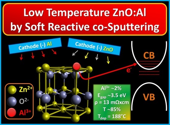
Controlled Al3+ Incorporation in the ZnO Lattice at 188 °C by Soft Reactive Co-Sputtering for Transparent Conductive Oxides

1
Department of Mathematical and Computational Sciences, Physics and Earth Sciences, University of Messina, V. le F. Stagno d’Alcontres 31, Messina 98166, Italy
2
National Research Council-Institute for Microelectronics and Microsystems (CNR-IMM), Zona industriale Strada VIII n°5, Catania 95121, Italy
*
Authors to whom correspondence should be addressed.
Submission received: 31 March 2016 / Revised: 25 May 2016 / Accepted: 27 May 2016 / Published: 3 June 2016
(This article belongs to the Special Issue Dye Sensitized Solar Cells)

Abstract

:
Transparent conductive oxide (TCO) layers, to be implemented in photo-anodes for dye-sensitized solar cells (DSCs), were prepared by co-deposition of ZnO and Al using pulsed-direct current (DC)-magnetron reactive sputtering processes. The films were deposited at low deposition temperatures (RT-188 °C) and at fixed working pressure (1.4 Pa) using soft power loading conditions to avoid intrinsic extra-heating. To compensate the layer stoichiometry, O2 was selectively injected close to the sample in a small percentage (Ar:O2 = 69 sccm:2 sccm). We expressly applied the deposition temperature as a controlling parameter to tune the incorporation of the Al3+ species in the targeted position inside the ZnO lattice. With this method, Aluminum-doped Zinc Oxide films (ZnO:Al) were grown following the typical wurtzite structure, as demonstrated by X-ray Diffraction analyses. A combination of micro-Raman, X-ray photoelectron spectroscopy (XPS) and spectroscopic ellipsometry (SE) analyses has shown that the incorporated host-atoms are Al3+ species in Zn2+ substitutional position; their amount increases following a direct monotonic trend with the deposition temperature. Correspondently, the c-axis strain into the layer decreases due to the progressive ordering of the lattice structure and reducing clustering phenomena. The maximum average Al content inside the film was ~2%, as measured by energy dispersive X-ray (EDX) spectroscopy, with a uniform distribution of the dopant species along the layer thickness traced by depth-profile XPS analyses. The optimised ZnO:Al layer, deposited at a rate of ~7 nm/min, exhibits high transmittance in the visible range (~85%) and low resistivity values (~13 mΩ × cm). The material therefore fulfils all the requirements to be candidate as TCO for low-cost DSCs on flexible substrates for large area technologies.

Graphical Abstract

1. Introduction

Transparent conductive oxide (TCO) films are currently of great importance for applications in transparent electrodes for flat panel displays [1], commercial semiconductors solar cells [2,3], hybrid solar cells [4,5] and organic light emitting diodes due to the high transmittance in the visible range (>80%), low electrical resistivity (10−2–10−4 Ω × cm), good adhesion to substrate and chemical inertness.
Among the others, dye-sensitized solar cells (DSCs) [6,7,8,9], being a third generation hybrid technology of large impact, benefits from the high performances of TCO [4,5,10,11]. Nowadays, indium tin oxide (ITO) films are predominant as TCO in practical applications. However, Al doped ZnO (ZnO:Al or AZO) films represent a potential alternative choice to ITO mainly because of their competitive electrical and optical properties, cheap and abundant raw materials, nontoxic nature, long term environmental stability and easy fabrication. In the DSC [2,3,8,10], the AZO films serve as collector of the electrons injected through the dye/TiO2 interface [12,13]. It could be even deposited at low temperature for applications on flexible substrates [14].
AZO layers can be prepared by various deposition techniques including pulsed laser deposition (PLD) [15], chemical vapor deposition (CVD) [16,17], sol-gel [18] and magnetron sputtering [19]. Among those approaches, magnetron sputtering from a composite target (98% ZnO + 2% Al2O3) has outstanding advantages such as simple apparatus, high deposition rates, low temperature and large deposition area. The method allows depositing doped ZnO films and assures contamination-free materials. Some literature works have also explored the possibility to deposit AZO conductive layers by co-sputtering using a double source (ZnO or Zn and Al or Al2O3) [19,20,21]. This configuration would in principle allow a tuning of the Al content in the AZO matrix. In this respect, it was however observed that a thermal budget at 400 °C is needed [20] in order to grow AZO layers with low resistivity. The annealing promotes Al3+ species replacing Zn2+ in the ZnO lattice. Nevertheless, due to the need of high thermal budgets, this method cannot be straightforwardly transferred to plastic substrates. Some other attempts were done to deposit doped materials at nominally low temperatures [14,21], but high power loadings, often combined with low chamber pressure, generate energetic ad-atoms that raise the effective temperature of the substrate during deposition (intrinsic heating). To our opinion, a good compromise needs to be targeted between the sputtering rate and the intrinsic substrate heating due to ad-atoms energy, in order to render the deposition process compatible with the use of low-cost substrates (e.g., plastics). Effective doping by substitutional Al, rather than by oxygen vacancies or other donor lattice defects, still remains crucial.
As the pervasive dissemination of DSCs technology needs to pass through a drastic cost reduction of the TCO, we focused our attention to an implementable approach able to produce ZnO:Al transparent conductive layers at low temperature. We thus propose a method based on direct current (DC) pulsed magnetron co-sputtering deposition under soft power loading using a double source (i.e., ZnO and Al) at moderate pressure (1.4 Pa) and real deposition temperatures below 200 °C. The deposition temperature, monitored directly on the sample surface by commercial thermo-strips (Racetech-Thermal indicator strips), was used as a parameter to incorporate an increasing amount of Al3+ species in the appropriate ZnO lattice position, during growth that allowed the dopant to be electrically active. The resulting material has optical-structural-electrical properties as good as those of a typical TCO film. The mutual correlation of these properties has been additionally discussed.

2. Experimental Section

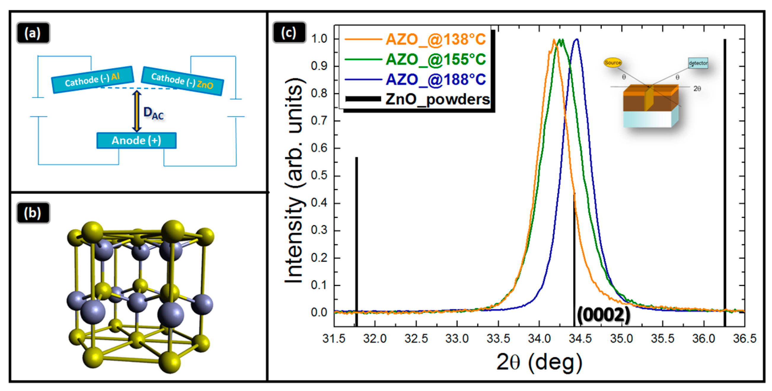
2.1. Deposition of the ZnO:Al Layers by Magnetron Direct Current Pulsed Sputtering

Aluminum-doped Zinc Oxide layers were deposited by using a DC Magnetron Sputter equipment (Kenosistec S.r.l.) in co-sputtering mode from separated Zinc Oxide and Aluminum targets plates (2 inch circular targets), placed in co-focal geometry. The depositions were done at real temperature < 200 °C (as measured on top of the sample by commercial thermo-strip, whose precision is ±1°) by using an Ar flow rate of 69 sccm, a sputtering power at the ZnO target of 40 W and sputtering power at the Al target of 20 W (above this threshold, clustering phenomena are observed in the sample). The power loading applied on the ZnO and Al targets was limited to ~2 W/cm2 and ~1 W/cm2, respectively, that avoided intrinsic heating of the substrate. A small additional supply of oxygen (2 sccm) was inflated into the chamber, in proximity to the sample surface, in order to compensate a slight deficit of oxygen in the deposited layer with respect to the target composition; the working pressure was 1.4 Pa. The deposition rate was of ~7 nm/min, and the thickness of the deposited material spans in the range of ~400–1000 nm, as determined by field emission-scanning electron microscopy (FE-SEM) analyses in cross section and further supported by spectroscopic ellipsometry (SE)/transmittance modelling which provided average values over large areas (~mm). Thereby, the spread of the thickness values at distances of 1.2 cm over the sample area was ~3%. Thermal treatments were done in situ by using a halogen short-wave lamp emitting in the range of 1.1–1.4 microns. A schematic of the chamber is shown in Figure 1a. Figure 1b shows the expected wurtzite structure of the ZnO lattice. We used the deposition temperature as the main parameter to tune the structure of the AZO layer (anode-cathode distance = 2 cm, rotation speed = five revolutions per minute (rpm), as resulted from the optimization procedure). Ex situ annealing were done in a horizontal oven filled with nitrogen and oxygen at flow rate of 78 sccm and 22 sccm, respectively.

2.2. Characterization Equipments

X-ray diffraction (XRD) (Bruker AXS Advanced X-ray Solutions GmbH, Karlsruhe, Germany) analyses were performed by using a D8-Discover Bruker AXS diffractometer, equipped with a Cu-Kα source and a thin film attachment (long soller slits). UV-VIS measurements were carried out by a Lambda 750 Perkin-Elmer spectrophotometer in the UV-VIS spectral range (PerkinElmer, Waltham, MA, USA). Spectra were recorded with a ±1nm resolution. FE-SEM (Zeiss, Oberkochen, Germany) images were collected with a Zeiss-Gemini 2 electron microscope operating at an accelerating voltage of 1.50 kV. To carry out energy dispersive X-ray (EDX) analysis, FE-SEM apparatus is coupled with a Quantax-EDX-spectrometer (Bruker AXS Advanced X-ray Solutions GmbH). The EDX detected pear-shaped dimension is about 0.7 micron. X-ray photoelectron spectroscopy (XPS) was carried out in ultra-high-vacuum (UHV) condition (about 1.33 × 10⁻⁷ Pa) using a Thermo Scientific Instrument (Thermo Fisher Scientific, Waltham, MA, USA) equipped with a monochromatic Al Kα source (hν = 1486.6 eV) and a hemispherical analyzer (spherical sector 180°). The constant-pass energy was set at 200 eV for survey scans and at 50 eV for the XPS high-resolution spectra. Being a surface technique, XPS is able to probe only a few monolayers. Hence, to estimate the composition of the layers in depth, it was necessary to progressively remove the surface layer using a scanning 3 KeV Ar+ ion gun, with a raster area of about 4 mm × 2 mm. SE data were collected using a J.A. Woollam VASE instrument (J.A. Woollam Co., Lincoln, NE, USA). Measurements were performed in a vertical configuration, which is better suited for transparent samples in order to measure on the same position ellipsometric and transmittance data. Optical spectra were recorded from 300 nm to 3200 nm at 55° and 65° incident angle values. The AZO layer was modeled by using one single Tauc-Lorentz and a Drude oscillators. Special care was taken to evaluate the optical constants for the glass substrate taking into account backside reflection and unpolarized light. Sheet resistance (Rs) measurements (Jandel Engineering Limited, Bedford, UK) were done by a four-point probe method; the layer resistivity was extracted from the sheet resistance values on the basis of the layer thickness (ρ = Rs × thickness). Micro-Raman measurements were carried at room temperature using a Horiba XploRA spectrometer equipped with a confocal microscope and a Peltier-cooled charge-coupled detector (CCD) (HORIBA Ltd., Fukuoka, Japan). The samples were excited using the 532 nm line from a solid-state laser and integrated for 80 s, using a 100X microscope objective. To check the uniformity of the deposited films, the measurements were acquired on some different portions of the samples.

3. Results and Discussion

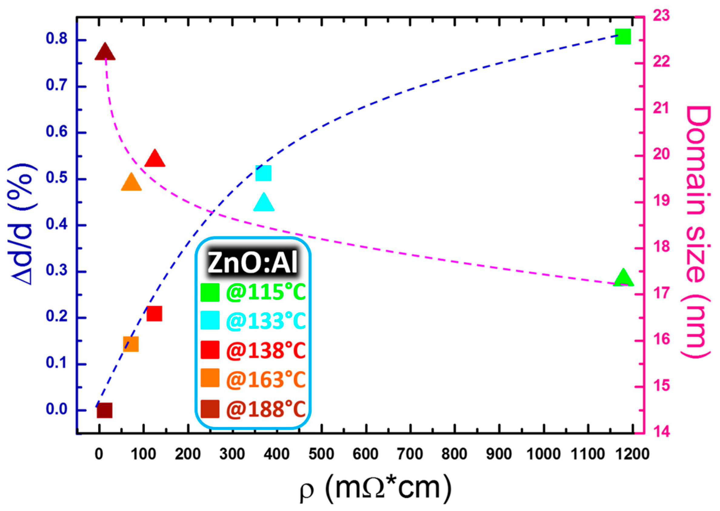
3.1. X-ray Diffraction Analysis

The crystallographic properties of the ZnO:Al layers were investigated by XRD analyses, using a symmetric configuration (2θ-ω). The diffraction patterns of layers prepared at different deposition temperature, namely 138, 155, and 188 °C, are shown in Figure 1c, with the maximum normalized to 1. The vertical bars refer to a random ZnO powder, with their relative scattering factors indicated by the bars height. All the patterns show a single contribution at 2θ ≅ 34.4°, which is related to the (0002) planes of the hexagonal wurtzite lattice (Figure 1b). Due to the acquisition geometry (2θ-ω), those lattice planes lie parallel to the sample surface, indeed with their growth direction along the c-axis of the wurtzite structure. The lack of the other intense contributions, which are expected in a random layer (see bars in Figure 1c), indicates a high texturing degree of the grown layers along the c-axis. This selectivity renders the layer structurally uniform in its extent. As a difference introduced by the deposition temperature modulation, the samples grown at temperature lower than 188 °C have the (0002) peak shifted leftwards with respect to the reference bar. The corresponding dspacing are 0.2623 nm and 0.2616 nm for the samples deposited at 138 °C and 155 °C, respectively. On the contrary, the ZnO:Al layer deposited at 188 °C has the peak associated to the (0002) planes at the position expected for an unstrained reference layer, whose dspacing is 0.2606 nm. This finding will be further discussed in what follows.

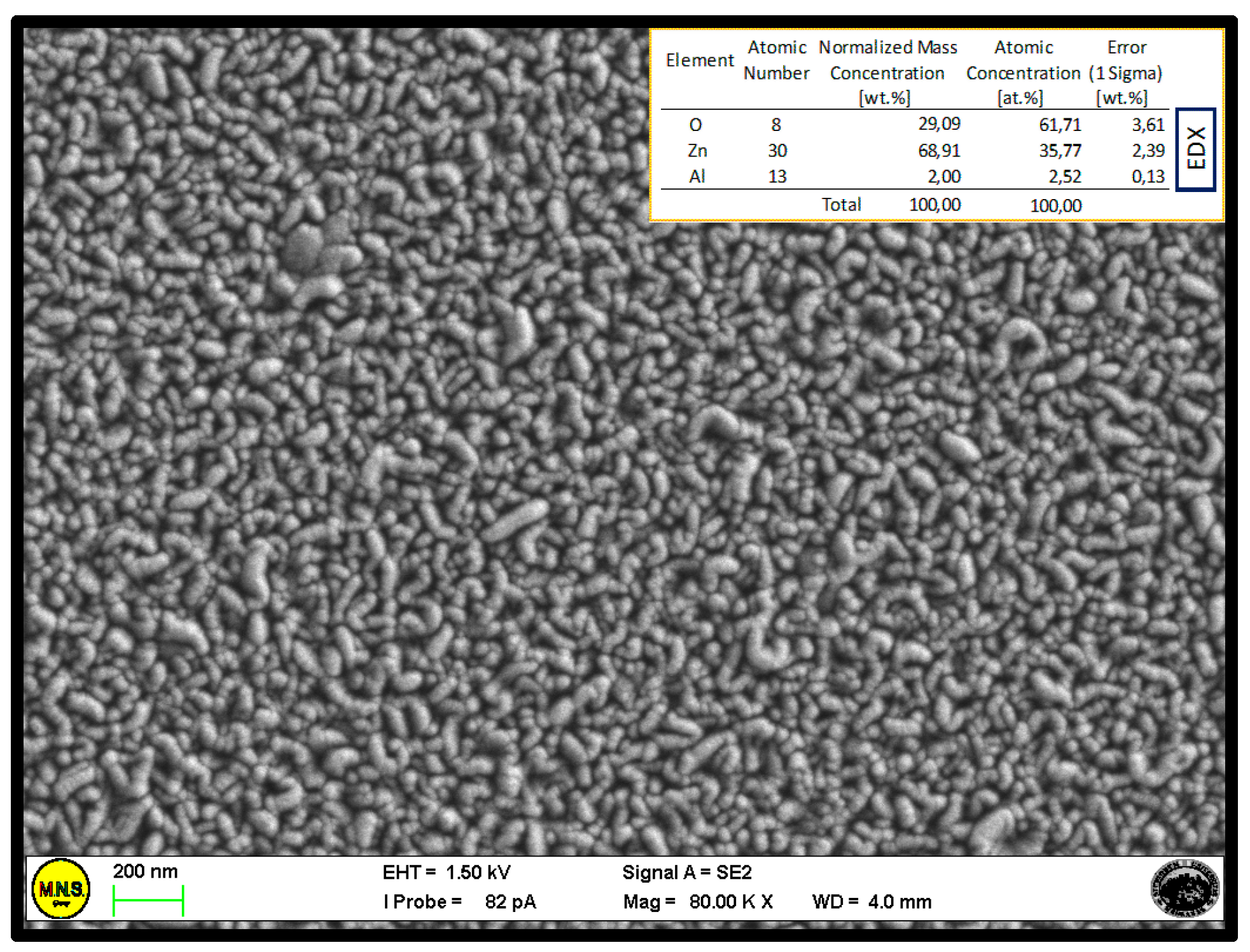
3.2. Field Emission-Scanning Electron Microscopy/Energy Dispersive X-ray Analyses

The morphology of all the films was investigated by FE-SEM. The average thickness of the ZnO:Al layer deposited at 188 °C, measured by FE-SEM images in cross section (not shown), was ~1 μm.
As can be appreciated in Figure 2, the material creates a uniform coating with homogeneous morphology that is fundamental to guarantee an effective charge transfer from the scaffold towards the TCO in a DSC. Spatial disuniformities in the layer thickness or in its surface roughness, with the eventual presence of deleterious protrusions, would affect the series resistance or generate parasitic currents (respectively) [10,22,23]. In situ EDX analyses provided an average atomic percentage of Al3+ inside the ZnO lattice of ~2%, (inset of Figure 2). Moreover, it was verified that the morphology does not significantly change from sample to sample.

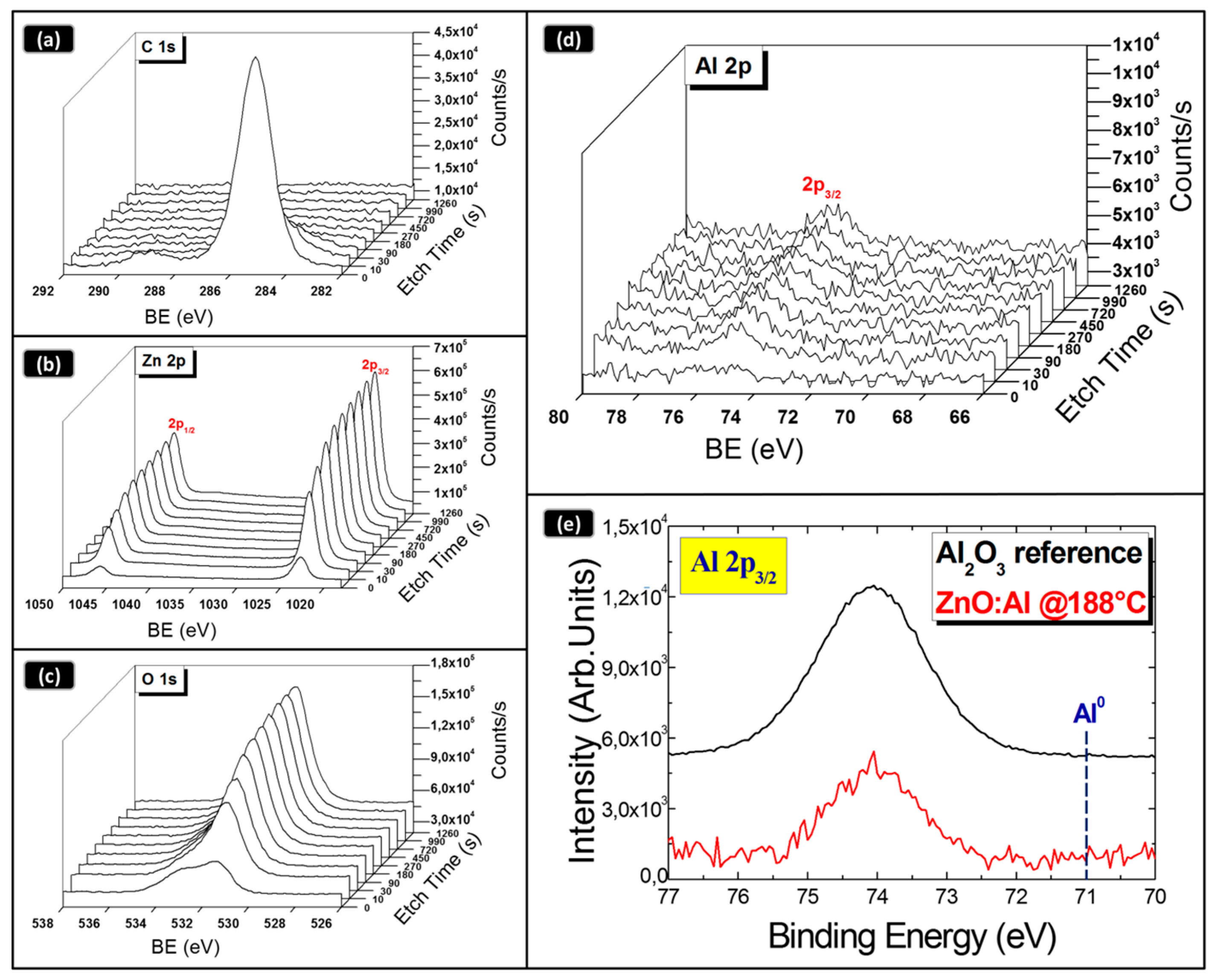
3.3. X-ray Photoelectron Spectroscopy Analysis

A detailed investigation on the composition of all the sputtered ZnO:Al layers was performed by XPS analyses. In particular, we collected a depth profile of all the involved species to study the composition along the layer thickness. The erosion rate was 16.2 nm/min, with the end-point given by the silicon atoms in the glass substrate.
The representative XPS wide scans of the AZO layer prepared at 188 °C, collected at different depth with respect to the film surface, are shown in Figure 3. The peaks due to C, Ar, Al, O and Zn were preliminary identified in the survey. High-resolution spectra were acquired to carry out appropriate composition and depth profile analyses. HR-XPS spectra for:
  • C 1s (at 284.7 eV);
  • O 1s (at 531.4 eV);
  • Zn 2p1/2 and 2p3/2 (at 1045 eV and 1022.8 eV respectively);
  • Al 2p3/2 (at 74.7 eV) regions are shown in Figure 4a–d.
We note that the surface of the material has a different composition with respect to the bulk, most likely due to surface contaminations. In fact, we found the presence of both –OH groups at binding energy (BE) of 532.5 eV and of carbonaceous species at about 284.7 eV (Figure 4a). The atomic percentage of all the species was estimated by the HR spectra, taking into account the relative atomic Scofield’s sensitivity factors [24]. The atomic composition does not vary significantly along the samples thickness. The estimated values are: Zn 52%, O 45%, Al 1.8% and C 1.2%, respectively (the relative values depend on the erosion procedure). Thereby, as a main result, the stoichiometry of the ZnO:Al layer is constant along the layer thickness, evidencing that a uniform Al content was inserted into the ZnO lattice during growth.
Figure 4e shows a detail of the XPS peak related to Al 2p3/2 taken on the ZnO:Al layer in comparison with what found in a Al2O3 reference material, to emphasize that the chemical environment of the Aluminum atoms does not show a metallic character (BE = 71 eV). On the contrary, the measured BE depicts a typical coordination of Al species by Oxygen atoms (BE = 74 eV).

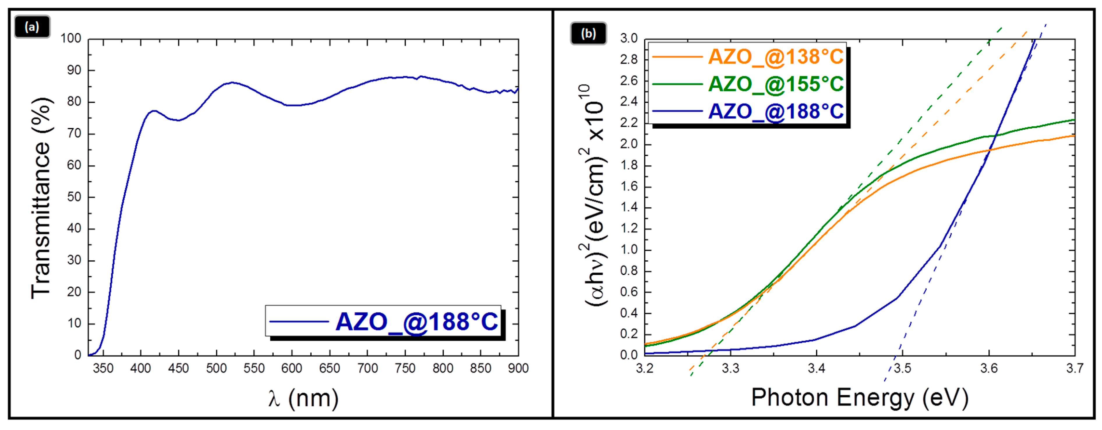
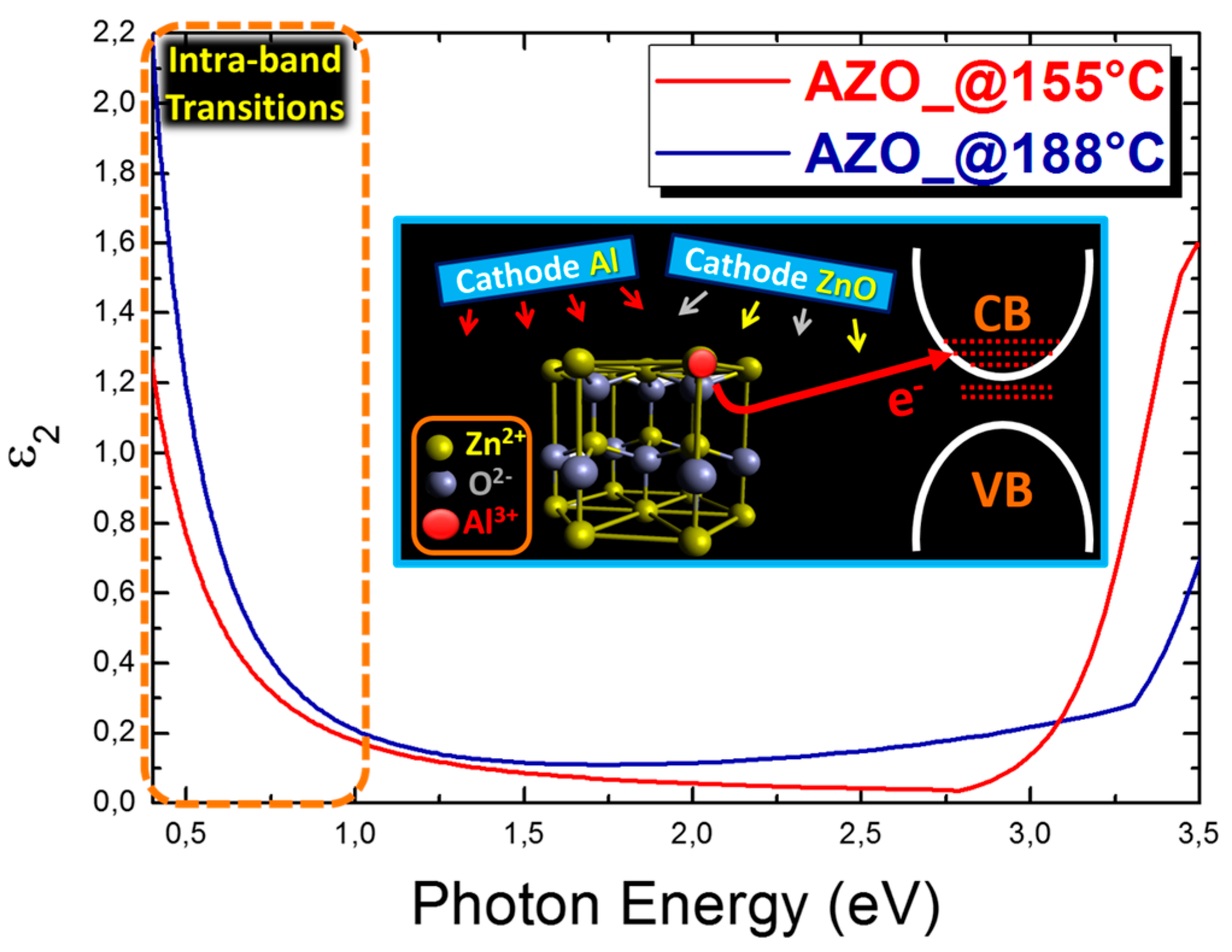
3.4. UV-VIS Measurements

The optical behavior of the deposited films was evaluated by investigation of the optical response of the material in the UV-VIS range. The mean transmittance of a 420 nm-thick AZO layer, deposited at 188 °C, settles around 85% in the visible range, as shown in Figure 5a. The optical band gap (Eg) of the films was estimated by the Tauc plot [25] of the absorption data for direct bandgap. With this procedure, the band gap is given by fitting the linear part of (αhν)2 vs. hν at the curve onset and by extracting the intercept with the x-axis. Figure 5b compares the Tauc plots of the ZnO:Al layers grown at different temperatures. The band gap values measured in the layer grown at 138 °C and at 155 °C are similar (~3.3 eV), whilst the layer grown at 188 °C exhibits a higher value, namely ~3.5 eV. The band gap widening was associated to the well-known Burstein-Moss effect [26], which derives from the electrons furnished by the dopant atoms populating states within the conduction band (CB). This occurs at high doping level and causes the Fermi level entering the CB. Our findings indeed provide a first indication on the effectiveness of the doping procedure by applying a deposition temperature of 188 °C.

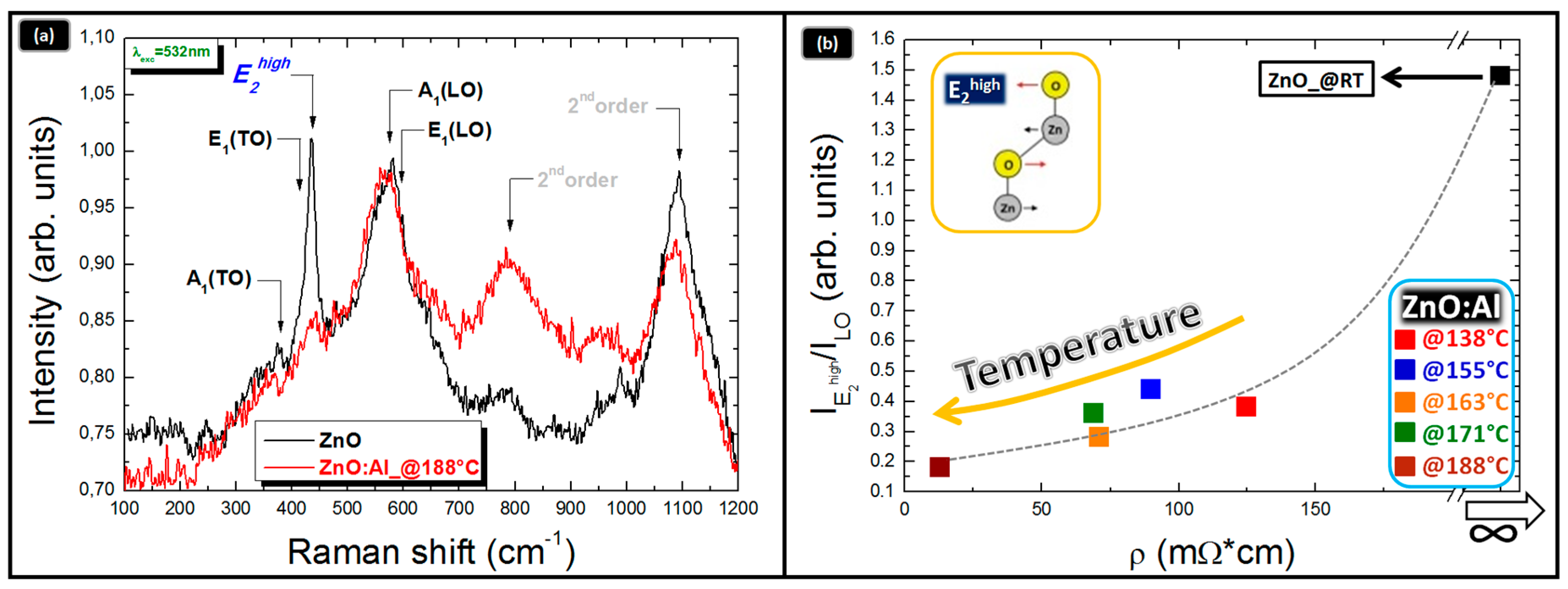
3.5. Micro-Raman Analysis

The optical results open a real perspective on the capability to replace Zn2+ with Al3+ species in the ZnO lattice by applying mild thermal budgets during co-sputtering (fixed all the other conditions). To closely enter the structure of the mixed material, Micro-Raman spectroscopy offered crucial details on the Al3+ location. The effects of the Al incorporation on the Raman peaks are shown in Figure 6a. The data refer to the ZnO:Al layer deposited at 188 °C. For comparison, a reference spectrum collected over an undoped ZnO layer is also reported. Vibrational modes in the ZnO lattice are expected at: ~380 cm−1 (ascribed to A1(TO) mode), ~413 cm−1 (ascribed to E1(TO) mode), ~440 cm−1 (ascribed to non-polar E 2 high mode, schematically represented in the inset of Figure 6b) and ~580-610 cm−1 (ascribed to A1(LO) and E1(LO)). Their positions are labeled in Figure 6a. Additionally, second orders of Raman modes are visible at ~800 cm−1 and 1100 cm−1 [27,28]. All those peaks account for the wurtzite C6v space group with four atoms per unit cell: among the 12 possible vibrational modes, only the A1, E1 and E2 are Raman-active. Furthermore, due to the ionic character of Zn-O bonds, polar modes (A1 and E1) exhibit a large splitting and second order modes [29].
According to the UV-VIS optical transmittance values, being in all samples > 70% at 532 nm (the excitation wavelength used to carry out the Raman measurements), we assess that the Raman beam has always probed the entire thickness of the ZnO:Al films. Moreover, to avoid specific thickness effects, the I E 2 high / I LO ratio (i.e., I LO indicated the longitudinal modes: A1(LO) and E1(LO)) was taken as a diagnostic parameter rather than E 2 high alone [28] and evaluated as a function of the deposition temperature. From the comparison between the spectra in Figure 6a it emerges that the E 2 high mode is much stronger in the pure ZnO sample with respect to what found in the ZnO:Al layer deposited at 188 °C. An analogous behavior was found in all the samples grown at the different temperatures. The reduction of the I E 2 high / I LO ratio by increasing the deposition temperature, as shown in Figure 6b, was related to structural changes in the lattice arrangement associated to the Al introduction into the ZnO matrix, compatible with Al3+ ions substituting Zn2+ species into the ZnO lattice [28]. Additional effects can be provided by the generation of oxygen-defects in the lattice [30,31]. Nevertheless, in this respect, an adjustment of the lattice structure is expected by increasing the deposition temperature rather than a progressive generation of oxygen defects, since the oxygen pressure in the chamber during sputtering was constant (as well as all the other deposition parameters except for the temperature).
On the basis of our findings we reasoned that the Al introduction into ZnO lattice is assisted by a controlled (external heating) slight increase of the temperature during deposition.

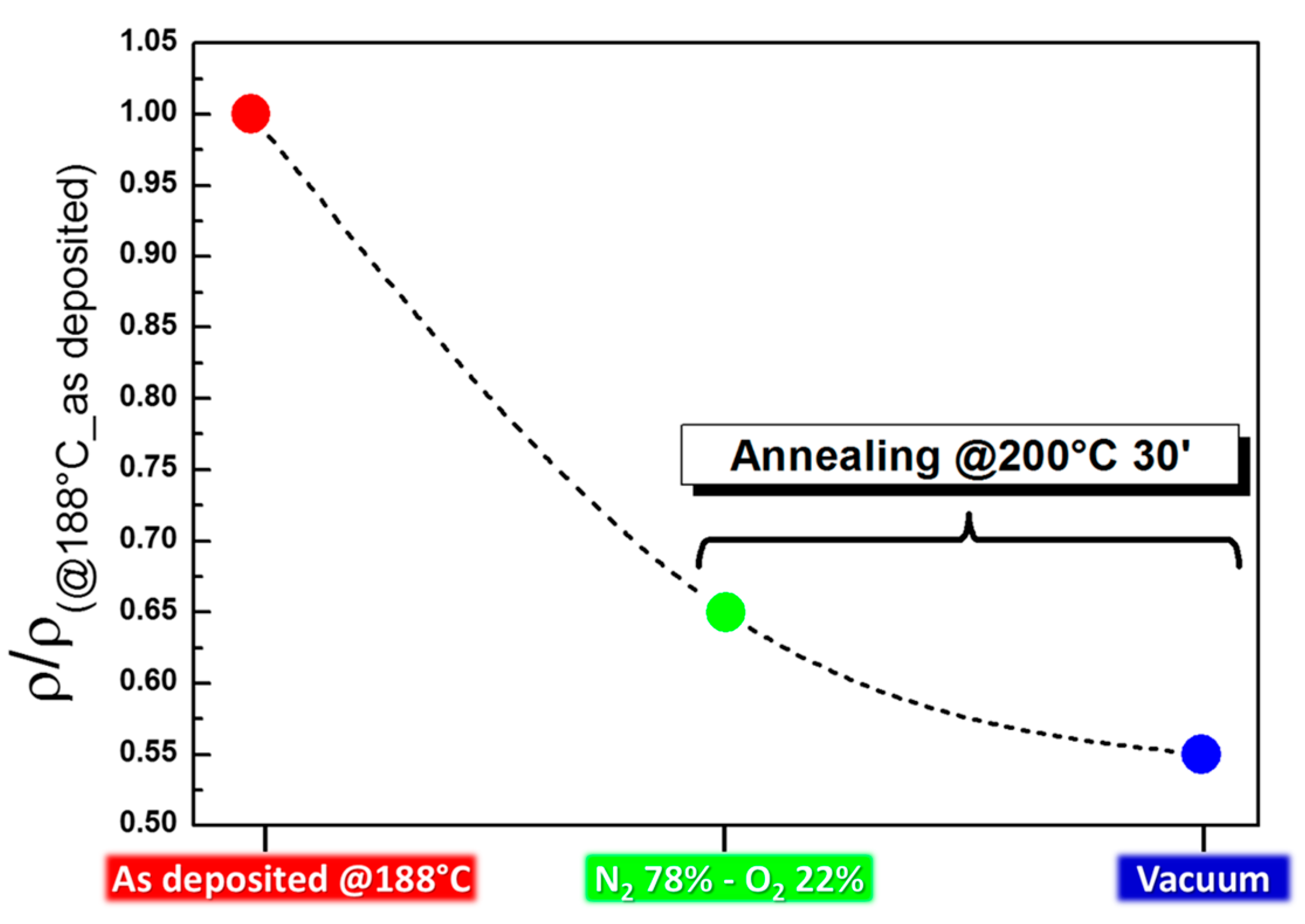
3.6. Electrical Characterizations

A monotonic reduction of the I E 2 high / I LO ratio was recorded as a function of the deposition temperature (RT < T < 200 °C), as shown in Figure 6b (T increases from right to left along x-axis) and Table 1. The data, correlated to the layer resistivity, elucidate that a progressive inhibition of the E 2 high Raman mode corresponds to a progressive improvement of the AZO layer conductivity [28,32]. We are inclined to exclude that the observed reduction of the I E 2 high / I LO parameter is due to an increase of residual lattice strain, as a possibility prospected in ref. [28]. This observation is based on our independent strain analyses done by XRD (see the following section). Thereby, we associate our findings to a progressive incorporation of Al3+ species in Zn2+ position, as an effect of increasing the deposition temperature. These structural properties render the incorporated species electrically active and thus able to increment the density of free carriers in the CB. As a matter of fact, the lowest resistivity value was measured in the AZO layer grown at 188 °C. The data are summarized in Table 1.
Since the resistivity value is affected not only by the carrier density but also by their scattering time (due to grain boundaries, aggregates, other defects, etc.), we additionally provide a correlation with the lattice strain and grain size. The average (crystallographic) domain size was measured by applying the Scherrer’s equation [33] to the full width at half maximum of the (0002) peak [28] and represented in the right panel of Figure 7 (right axis, pink curve). In addition to the grain size (related to the density of grain boundaries), the evaluation of the residual strain in the ZnO:Al lattice was provided as an indirect measure of the average effect of the presence of extended defects in the ZnO:Al lattice. The residual strain was evaluated by measuring the (0002) lattice planes distances (XRD, Figure 1) as compared to reference values (unstrained ZnO lattice) [28]. It was expressed as Δd/d (%) and plotted as a function of the layer resistivity in Figure 7 (left axis, blue curve). We note a decreasing trend of the strain measured along the c-axis accompaining the resistivity reduction, towards a zero strain condition (unstrained: Δd/d (%) = 0) corresponding to the most conductive layer (188 °C).
This result gives evidence of a progressive reduction of the defects inside the wurtzite lattice, likely associated to less severe Al-based clustering (e.g., Al2O3) and/or to atomic disorder. Since oxygen vacancies and substitutional Al can both affect the intensity of the E 2 high Raman mode, it was crucial to establish that the deposition temperature (at fixed oxygen pressure) causes a reduction of the residual strain in the film. This observed behavior argues in favor of Al3+ substituting Zn2+, with direct positive impact on the layer resistivity.
On the other hand, the eventual formation of charged V 0 2 + states (under non equilibrium conditions), with the consequent injection of electrons into the ZnO CB [30,34], would imply that the Zn-Zn bonding distances around the defect would experience an outwards stretching [30]. If this relaxation was extended in average to the entire lattice, this should cause a shift of the diffraction peaks towards lower angles. This is the opposite of what experimentally found, since the peak systematically moves upwards in the direction of the unstrained reference if the deposition temperature is increased (<200 °C). A major defective material when increasing the deposition temperature is also counterintuitive. Moreover, in all the deposition process, a slight supply of oxygen was used to avoid growth condition under deficiency of oxygen [31]. All those consideration are in favor of Al atoms rather replacing Zn in a certain (even partial with respect to the 2 at% introduced) amount. To further reinforce our conclusions, we performed mild ex situ annealing (at 200 °C) on the as deposited sample, using dry air (N2:O2 = 78 sccm:22 sccm) vs. vacuum conditions (1.33 Pa). The presence of oxygen in the annealing ambient is expected to impact on the concentration of oxygen vacancies. Nonetheless, in both cases the sample experienced an improvement of the electrical performances, with the resistivity reducing to 8.5 and 7 mΩ × cm in air and vacuum, respectively (Figure 8). This finding was thus correlated to a further adjustment of the lattice structure, including better positioning of substitutional Al species.
Figure 7 additionally shows (pink curve) an increase of the ZnO:Al domain size, which consistently goes in the direction of a better carrier transport. We indeed argue that the resistivity reduction also benefits from less severe carrier scattering events from grain boundary or extended defects.
To have further details on the optical-electrical response of the doped material, we used SE measurements. Figure 9 shows the imaginary part of the dielectric constant, ε2, for two samples grown at 155 °C and 188 °C. It is of particular interest the behavior of ε2 in the infrared region (<1 eV). In particular, we observe that the material deposited at 188 °C shows a typical behavior from intra-band transitions experienced by the electrical carriers [35]. This was associated to the electrons, provided by the dopant atoms, which enter in the CB with their energetic levels and in total behave as a free electron gas, as translated in the applied Drude’s model to fit the raw data. Although high doping levels tend to affect the transmittance of the material, we emphasize that the average transmittance measured on this sample stays as high as 85% (Figure 5a). On the other hand, the ZnO:Al deposited at 155 °C exhibits a lower absorption in the Infra-Red (IR) region, depicting a material with a lower amount of free electrons charges. The analysis gives a further clear evidence of the effectiveness of our methodology on the capability to tune the Al3+ species incorporation in the ZnO lattice as substitutional dopant. Consistently with the Tauc’s plot results (Figure 5b), the onset of the absorption behavior over the band gap is clearly triggered at higher energies in the sample deposited at 188 °C (right part of the curves in Figure 9).

4. Conclusions

We have explored a sputtering approach at low temperature and at soft power loading in compensated oxygen ambient to effectively dope ZnO layers with Aluminum atoms such to gain convenient optical and electrical responses. The approach is based on the co-deposition of the component materials (ZnO and Al) at T < 200 °C by using a co-focal geometry. The deposition conditions settled a compromise between power loading and working pressure in order to provide relatively high deposition rate coupled with low intrinsic substrate heating. We currently pushed the deposition process at a level of maturity that provides the material with:
(1)
Al3+ species effectively incorporated in the ZnO structure with negligible residual strain;
(2)
uniform ZnO:Al stoichiometry at least over 1 μm of grown thickness;
(3)
optical bandgap of ~3.5 eV;
(4)
~85% transmittance in the visible range;
(5)
deposition rate as high as ~7 nm/min.
The overall structural optimization, as achieved at a real deposition temperature of 188 °C (measured on the sample surface), allowed producing a material with resistivity as low as ~13 mΩ × cm, namely 13 Ω/sq in 1 μm. The large potentiality of our approach, in summary, resides in:
(1)
avoiding intrinsic overheating and instead using a mild controlled extrinsic heating;
(2)
compensating oxygen deficiency to limit the formation of oxygen defects;
(3)
guaranteeing a uniform incorporation of Al during growth.
All those advantages add up with the availability of an independent Al source for complementary stacked materials (e.g., Al or Al2O3). They represent a progress in the material reliability and stability for application on low cost substrates.

Acknowledgments

The authors thank Stefano Perugini, Giovanni Barbieri and Carlo Aliberti (Kenosistec S.r.l.) for the technical collaboration and assistance on the sputtering equipments. This work was partially supported by the Italian Project “Elettronica su Plastica per Sistemi Smart disposable” (Electronics on Plastics for “Smart disposable” Systems) funded by Ministero Istruzione Università e Ricerca (MIUR) to the Distretto Tecnologico Sicilia Micro e Nano Sistemi by means of the Italian Program PON02_00355_3416798.

Author Contributions

Alessandra Alberti and Fortunato Neri conceived and designed the experiment, equally contributing to the data interpretation. Salvatore Sanzaro performed the deposition of all the materials discussed in the paper and dealt with most of the data analyses. Antonino La Magna critically revised the manuscript and contributed to data interpretation. Enza Fazio performed Micro-Raman, depth-profile-XPS and FE-SEM analyses. Giovanna Pellegrino performed surface HR-XPS and UV-VIS analyses. XRD measurements were done by Emanuele Smecca. Giovanni Mannino performed SE measurements and data modeling.

Conflicts of Interest

The authors declare no conflict of interest.

Abbreviations

TCOTransparent conductive oxide
AZOAl doped ZnO
ITOIndium Tin Oxide
PLDPulsed laser deposition
CVDChemical vapor deposition
DCDirect current
DSCDye-sensitized solar cells
XRDX-ray diffraction
FE-SEMField emission-scanning electron microscopy
EDXEnergy dispersive X-ray
HRHigh resolution
XPSX-ray photoelectron spectroscopy
UHVUltra high vacuum
CCDCharge-coupled detector
SESpectroscopic ellipsometry
BEBinding energy
CBConduction band
RsSheet resistance
sccmstandard cubic centimeter minute
rpmrevolutions per minute

References

  1. Ko, Y.D.; Kim, J.Y.; Joung, H.C.; Ahn, S.H.; Jang, K.S.; Lee, Y.J.; Yi, J. Low temperature deposited transparent conductive ITO and IZTO films for flat panel display applications. J. Ceram. Process. Res. 2013, 14, 183–187. [Google Scholar]
  2. Fortunato, E.; Ginley, D.; Hosono, H.; Paine, D.C. Transparent conducting oxides for photovoltaics. MRS Bull. 2007, 32, 242–247. [Google Scholar] [CrossRef]
  3. Abrinaei, F.; Shirazi, M.; Hosseinnejad, M.T. Investigation of growth dynamics of nanostructured aluminum doped zinc oxide thin films deposited for the solar cell applications. J. Inorg. Organomet. Polym. 2016, 26, 233–241. [Google Scholar] [CrossRef]
  4. Dong, P.; Zhu, Y.; Zhang, J.; Hao, F.; Wu, J.; Lei, S.; Lin, H.; Hauge, R.H.; Tour, J.M.; Lou, J. Vertically aligned carbon nanotubes/graphene hybrid electrode as a TCO- and Pt-Free flexible cathode for application in solar cells. J. Mater. Chem. A 2014, 2, 20902–20907. [Google Scholar] [CrossRef]
  5. Huang, M.; Hameiri, Z.; Gong, H.; Wong, W.C.; Aberle, A.G.; Mueller, T. Novel hybrid electrode using transparent conductive oxide and silver nanoparticle mesh for silicon solar cell applications. Energy Procedia 2014, 55, 670–678. [Google Scholar] [CrossRef]
  6. Grätzel, M. Solar energy conversion by dye-sensitized photovoltaic cells. Inorg. Chem. 2005, 44, 6841–6851. [Google Scholar] [CrossRef] [PubMed]
  7. Grisorio, R.; De Marco, L.; Giannuzzi, R.; Gigli, G.; Suranna, G.P. Molecular engineering of largely π-extended metal-free sensitizers containing benzothiadiazole units: Approaching 10% efficiency dye-sensitized solar cells using iodine-based electrolytes. Dye. Pigment. 2016, 131, 282–292. [Google Scholar] [CrossRef]
  8. Chou, T.P.; Zhang, Q.; Cao, G. Effects of dye loading conditions on the energy conversion efficiency of ZnO and TiO2 dye-sensitized solar cells. J. Phys. Chem. C 2007, 111, 18804–18811. [Google Scholar] [CrossRef]
  9. Noh, J.H.; Han, H.S.; Lee, S.; Kim, D.H.; Park, J.H.; Park, S.; Kim, J.Y.; Jung, H.S.; Hong, K.S. A newly designed Nb-doped TiO2/Al-doped ZnO transparent conducting oxide multilayer for electrochemical photoenergy conversion devices. J. Phys. Chem. C 2010, 114, 13867–13871. [Google Scholar] [CrossRef]
  10. Alberti, A.; De Marco, L.; Pellegrino, G.; Condorelli, G.G.; Giannuzzi, R.; Scarfiello, R.; Manca, M.; Spinella, C.; Gigli, G.; La Magna, A. A combined strategy to realize efficient photoelectrodes for low temperature fabrication of dye solar cells. ACS Appl. Mater. Interfaces 2014, 6, 6425–6433. [Google Scholar] [CrossRef] [PubMed]
  11. Alberti, A.; Pellegrino, G.; Condorelli, G.G.; Bongiorno, C.; Morita, S.; La Magna, A.; Miyasaka, T. Efficiency enhancement in ZnO:Al-based dye-sensitized solar cells structured with sputtered TiO2 blocking layers. J. Phys. Chem. C 2014, 118, 6576–6585. [Google Scholar] [CrossRef]
  12. Sanzaro, S.; Pellegrino, G.; Smecca, E.; Malandrino, G.; Catalano, R.; La Magna, A.; Alberti, A. Deposition of ZnO:Al/TiO2 Bi-Layers at Low Temperature by Reactive Sputtering for Application as Photoanodes in Dye-Sensitized Solar Cells; Activity Report 2014-Dip. Di Fisica; University of Messina: Messina, Italy, 2014; pp. 87–90. [Google Scholar]
  13. Pellegrino, G.; Condorelli, G.G.; De Rossi, F.; Brown, T.; Giovenale, F.; Bongiorno, C.; Alberti, A. Thermally induced structural modifications of nano-sized anatase films and the effects on the dye-TiO2 surface interactions. Appl. Surf. Sci. 2014, 296, 69–78. [Google Scholar] [CrossRef]
  14. Chung, Y.M.; Moon, C.S.; Jung, M.J.; Han, J.G. The low temperature synthesis of Al doped ZnO films on glass and polymer using magnetron co-sputtering: Working pressure effect. Surf. Coat. Technol. 2005, 200, 936–939. [Google Scholar] [CrossRef]
  15. Liu, Y.D.; Zhao, L.; Lian, J.S. Al-doped ZnO films by pulsed laser deposition at room temperature. Vacuum 2006, 81, 18–21. [Google Scholar] [CrossRef]
  16. Hu, J.; Gordon, R.G. Textured aluminum-doped zinc oxide thin films from atmospheric pressure chemical-vapor deposition. J. Appl. Phys. 1992, 71, 880–890. [Google Scholar] [CrossRef]
  17. Shirahata, T.; Kawaharamura, T.; Fujita, S.; Orita, H. Transparent conductive zinc-oxide-based films grown at low temperature by mist chemical vapor deposition. Thin Solid Films 2015, 597, 30–38. [Google Scholar] [CrossRef]
  18. Kim, Y.S.; Tai, W.P. Electrical and optical properties of Al-doped ZnO thin films by sol-gel process. Appl. Surf. Sci. 2006, 253, 4911–4916. [Google Scholar] [CrossRef]
  19. Li, Q.H.; Zhu, D.; Liu, W.; Liu, Y.; Ma, X.C. Optical properties of Al-doped ZnO thin films by ellipsometry. Appl. Surf. Sci. 2008, 254, 2922–2926. [Google Scholar] [CrossRef]
  20. Deng, Z.; Huang, C.; Huang, J.; Wang, M.; He, H.; Wang, H.; Cao, Y. Effects of Al content on the properties of ZnO:Al films prepared by Al2O3 and ZnO co-sputtering. J. Mater. Sci. Mater. Electron 2010, 21, 1030–1035. [Google Scholar] [CrossRef]
  21. Gorgulla, A.; Ertel, D.P.; Steyer, M.; Hahn, G.; Terheiden, B. Effect of Al concentration analyzed by ICP-OES on the structural, electrical and optical properties of co-sputtered ZnO:Al films. Energy Procedia 2015, 77, 687–693. [Google Scholar] [CrossRef]
  22. Caramori, S.; Cristino, V.; Boaretto, R.; Argazzi, R.; Bignozzi, C.A.; Di Carlo, A. New components for dye-sensitized solar cells. Int. J. Photoenergy 2010, 2010. [Google Scholar] [CrossRef]
  23. Grätzel, M. Photoelectrochemical cells. Nature 2001, 414, 338–344. [Google Scholar] [CrossRef] [PubMed]
  24. Scofield, J.H. Hartree-Slater subshell photoionization cross-sections at 1254 and 1487 eV. J. Electron. Spectrosc. Relat. Phenom. 1976, 8, 129–137. [Google Scholar] [CrossRef]
  25. Karunagaran, B.; Kim, K.; Mangalaraj, D.; Yi, J.; Velumani, S. Structural, optical and Raman scattering studies on DC magnetron sputtered titanium dioxide thin films. Solar Energy Mater. Solar Cells 2005, 88, 199–208. [Google Scholar] [CrossRef]
  26. Burstein, E. Anomalous optical absorption limit in InSb. Phys. Rev. 1954, 93, 632. [Google Scholar] [CrossRef]
  27. Ozgur, U.; Alivov, Y.I.; Liu, C.; Teke, A.; Reshchikov, M.A.; Dogan, S.; Avrutin, V.; Cho, S.J.; Morkoc, H.J. A comprehensive review of ZnO materials and devices. J. Appl. Phys. 2005, 98. [Google Scholar] [CrossRef]
  28. Russo, V.; Ghidelli, M.; Gondoni, P.; Casari, C.S.; Li Bassi, A. Multi-wavelength Raman scattering of nanostructured Al-doped zinc oxide. J. Appl. Phys. 2014, 115. [Google Scholar] [CrossRef]
  29. Reparaz, J.S.; Muniz, L.R.; Wagner, M.R.; Goñi, A.R.; Alonso, M.I.; Hoffmann, A.; Meyer, B.K. Reduction of the transverse effective charge of optical phonons in ZnO under pressure. Appl. Phys. Lett. 2010, 96. [Google Scholar] [CrossRef]
  30. Lany, S.; Zunger, A. Anion vacancies as a source of persistent photoconductivity in II-VI and chalcopyrite semiconductors. Phys. Rev. B 2005, 72. [Google Scholar] [CrossRef]
  31. Lany, S.; Zunger, A. Dopability, intrinsic conductivity, and nonstoichiometry of transparent conducting oxides. Phys. Rev. Lett. 2007, 98. [Google Scholar] [CrossRef] [PubMed]
  32. El Manouni, A.; Manjón, F.J.; Mollar, M.; Marí, B.; Gómez, R.; López, M.C.; Ramos-Barrado, J.R. Effect of aluminium doping on zinc oxide thin films grown by spray pyrolysis. Superlattices Microstruct. 2006, 39, 185–192. [Google Scholar] [CrossRef]
  33. Cullity, B.D. Elements of X-ray Diffraction, 2nd ed.; Addison-Wesley: Boston, MA, USA, 1978; p. 102. [Google Scholar]
  34. Clark, S.J.; Robertson, J.; Lany, S.; Zunger, A. Intrinsic defects in ZnO calculated by screened exchange and hybrid density functionals. Phys. Rev. B 2010, 81. [Google Scholar] [CrossRef]
  35. Maghanga, C.M.; Niklasson, G.A.; Granqvist, C.G. Optical properties of sputter deposited transparent and conducting TiO2:Nb films. Thin Solid Films 2009, 518, 1254–1258. [Google Scholar] [CrossRef]
Figure 1. (a) Schematic of the co-focal geometry; (b) Wurtzite structure; and (c) 2θ-ω X-ray diffraction (XRD) patterns of different Al doped ZnO (AZO) samples deposited at low temperature (T < 200 °C).
Energies 09 00433 g001
Figure 2. Field emission-scanning electron microscopy (FE-SEM) analysis of the AZO layer deposited by co-sputtering in co-focal geometry at 188 °C. Inset: the atomic percentages of the species revealed by energy dispersive X-ray (EDX) probe.
Energies 09 00433 g002
Figure 3. X-ray photoelectron spectroscopy (XPS) wide scans of AZO layers at different depth.
Energies 09 00433 g003
Figure 4. XPS depth profile analyses of the AZO layer deposited by co-sputtering in co-focal geometry at 188 °C: (a) C 1s; (b) O 1s; (c) Zn 2p; (d) Al 2p3/2 spectra; and (e) Al 2p3/2 spectrum taken on the AZO layer and on a reference Al2O3 material. Al0 is the expected peak position for a metallic layer.
Energies 09 00433 g004
Figure 5. (a) Transmittance spectra of an AZO sample deposited at 188 °C; and (b) Tauc plots of AZO layers deposited at different temperatures to evaluate the optical band gap.
Energies 09 00433 g005
Figure 6. (a) Typical Micro-Raman spectra of ZnO layers (-) undoped and (-) doped with Al at 188 °C; (b) monotonic decrease of the I E 2 high / I LO intensity ratio as a function of the layer resistivity ρ.
Energies 09 00433 g006
Figure 7. Structural properties evaluated by XRD analysis correlated to the electrical behavior of the AZO layers. On the left side (blue curve): strain along the c-axis; on the right side (pink curve): crystallographic domain size. The different colors of the data points correspond to different deposition temperatures.
Energies 09 00433 g007
Figure 8. The effect of adding ex situ heating on the layer resistivity. Note that the presence of oxygen species in the annealing ambient does not negatively affect the layer conductivity.
Energies 09 00433 g008
Figure 9. Spectroscopic ellipsometry (SE) measurements giving the dielectric constants ε2 as a function of the photon energy. Note the absorption in the Infra-Red (IR) region enhanced in the AZO layer deposited at 188 °C, which represents a marker for intra-band transitions as a consequence of the Fermi level entering the conduction band (CB) (inset).
Energies 09 00433 g009
Table 1. Micro-Raman and resistivity data.
Sample E 2 h i g h / L O Intensity RatioResistivity (mΩ × cm)Conductivity (S/cm)
AZO_@138 °C0.381258.00
AZO_@155 °C0.449011.11
AZO_@163 °C0.366914.49
AZO_@171 °C0.287114.08
AZO_@188 °C0.181376.92

