A Post-Treatment Method to Enhance the Property of Aerosol Jet Printed Electric Circuit on 3D Printed Substrate

 ,
,
Abstract
:
1. Introduction
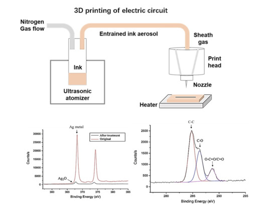
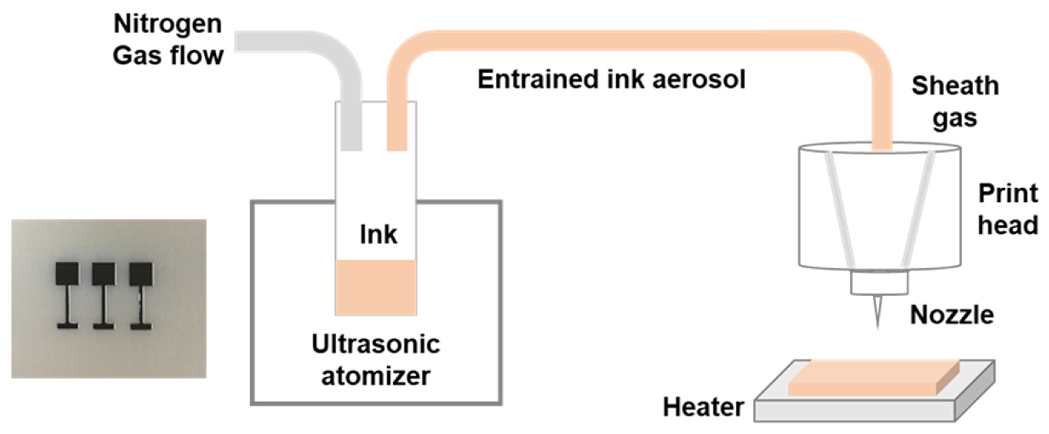
2. Materials and Methods
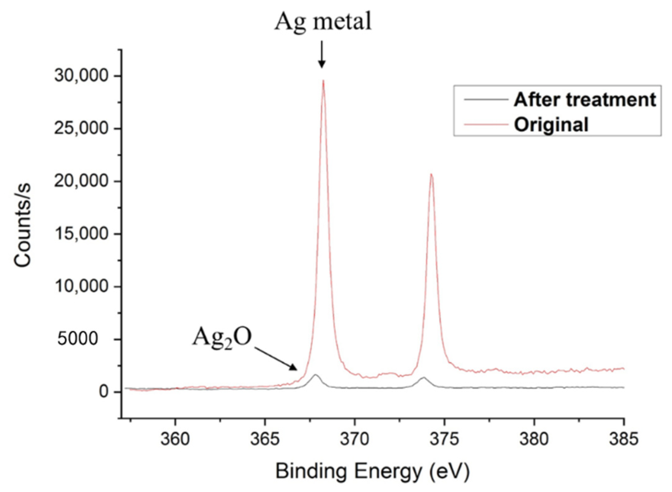
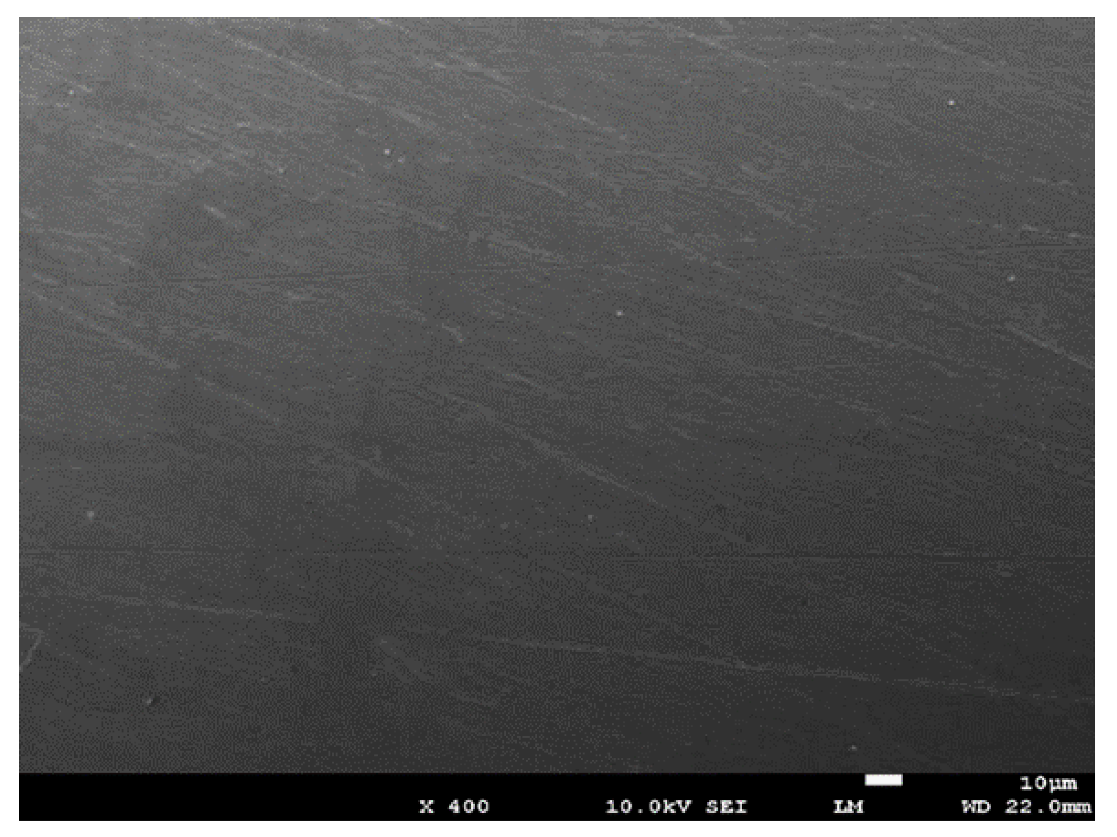
3. Results and Discussion
4. Conclusions
Author Contributions
Funding
Acknowledgments
Conflicts of Interest
References
- Calvert, P. Inkjet Printing for Materials and Devices. Chem. Mater. 2001, 13, 3299–3305. [Google Scholar] [CrossRef]
- Singh, M.; Haverinen, H.M.; Dhagat, P.; Jabbour, G.E. Inkjet Printing-Process and Its Applications. Adv. Mater. 2010, 22, 673–685. [Google Scholar] [CrossRef] [PubMed]
- Seifert, T.; Sowade, E.; Roscher, F.; Wiemer, M.; Gessner, T.; Baumann, R.R. Additive Manufacturing Technologies Compared: Morphology of Deposits of Silver Ink Using Inkjet and Aerosol Jet Printing. Ind. Eng. Chem. Res. 2015, 54, 769–779. [Google Scholar] [CrossRef]
- Najmon, J.C.; Raeisi, S.; Tovar, A. Review of Additive Manufacturing Technologies and Applications in the Aerospace Industry. In Additive Manufacturing for the Aerospace Industry; Froes, F., Boyer, R., Eds.; Elsevier: Amsterdam, The Netherlands, 2019; pp. 7–31. [Google Scholar]
- Dilberoglu, U.M.; Gharehpapagh, B.; Yaman, U.; Dolen, M. The Role of Additive Manufacturing in the Era of Industry 4.0. Procedia Manuf. 2017, 11, 545–554. [Google Scholar] [CrossRef]
- Yuan, S.; Shen, F.; Chua, C.K.; Zhou, K. Polymeric composites for powder-based additive manufacturing: Materials and applications. Prog. Polym. Sci. 2019, 91, 141–168. [Google Scholar] [CrossRef]
- Krebs, F.C. Polymer solar cell modules prepared using roll-to-roll methods: Knife-over-edge coating, slot-die coating and screen printing. Sol. Energy Mater. Sol. Cells 2009, 93, 465–475. [Google Scholar] [CrossRef]
- Chen, B.; Jiang, Y.; Tang, X.; Pan, Y.; Hu, S. Fully Packaged Carbon Nanotube Supercapacitors by Direct Ink Writing on Flexible Substrates. ACS Appl. Mater. Interfaces 2017, 9, 28433–28440. [Google Scholar] [CrossRef]
- Sirringhaus, H.; Kawase, T.; Friend, R.H.; Shimoda, T.; Inbasekaran, M.; Wu, W.; Woo, E.P. High-Resolution Inkjet Printing of All-Polymer Transistor Circuits. Science 2000, 290, 2123–2126. [Google Scholar] [CrossRef] [Green Version]
- Jones, C.S.; Lu, X.; Renn, M.; Stroder, M.; Shih, W.-S. Aerosol-jet-printed, high-speed, flexible thin-film transistor made using single-walled carbon nanotube solution. Microelectron. Eng. 2010, 87, 434–437. [Google Scholar] [CrossRef]
- Shaheen, S.E.; Radspinner, R.; Peyghambarian, N.; Jabbour, G.E. Fabrication of bulk heterojunction plastic solar cells by screen printing. Appl. Phys. Lett. 2001, 79, 2996–2998. [Google Scholar] [CrossRef]
- Pardo, D.A.; Jabbour, G.E.; Peyghambarian, N. Application of Screen Printing in the Fabrication of Organic Light-Emitting Devices. Adv. Mater. 2000, 12, 1249–1252. [Google Scholar] [CrossRef]
- Zhang, H.; Moon, S.K.; Ngo, T.H. 3D Printed Electronics of Non-contact Ink Writing Techniques: Status and Promise. Int. J. Precis. Eng. Manuf. Technol. 2019, 7, 511–524. [Google Scholar] [CrossRef]
- Min, K.; Kim, H.-C.; Choi, J.-W.; Lee, I.H. A review on 3D printed smart devices for 4D printing. Int. J. Precis. Eng. Manuf. Technol. 2017, 4, 373–383. [Google Scholar] [CrossRef]
- Park, S.-I.; Quan, Y.-J.; Kim, S.-H.; Kim, H.; Kim, S.; Chun, D.-M.; Lee, C.S.; Taya, M.; Chu, W.-S.; Ahn, S.-H. A review on fabrication processes for electrochromic devices. Int. J. Precis. Eng. Manuf. Technol. 2016, 3, 397–421. [Google Scholar] [CrossRef]
- Wilkinson, N.J.; Smith, M.A.A.; Kay, R.W.; Harris, R.A. A review of aerosol jet printing—A non-traditional hybrid process for micro-manufacturing. Int. J. Adv. Manuf. Technol. 2019, 105, 4599–4619. [Google Scholar] [CrossRef] [Green Version]
- Smith, M.; Choi, Y.S.; Boughey, C.; Kar-Narayan, S. Controlling and assessing the quality of aerosol jet printed features for large area and flexible electronics. Flex. Print. Electron. 2017, 2, 015004. [Google Scholar] [CrossRef]
- Zhang, H.; Moon, S.K.; Ngo, T.H. Hybrid Machine Learning Method to Determine the Optimal Operating Process Window in Aerosol Jet 3D Printing. ACS Appl. Mater. Interfaces 2019, 11, 17994–18003. [Google Scholar] [CrossRef]
- Clifford, B.; Beynon, D.; Phillips, C.; Deganello, D. Printed-Sensor-on-Chip devices—Aerosol jet deposition of thin film relative humidity sensors onto packaged integrated circuits. Sens. Actuators B Chem. 2018, 255, 1031–1038. [Google Scholar] [CrossRef] [Green Version]
- Cantù, E.; Tonello, S.; Abate, G.; Uberti, D.; Sardini, E.; Serpelloni, M. Aerosol Jet Printed 3D Electrochemical Sensors for Protein Detection. Sensors 2018, 18, 3719. [Google Scholar] [CrossRef] [Green Version]
- Cao, C.; Andrews, J.B.; Franklin, A.D. Completely Printed, Flexible, Stable, and Hysteresis-Free Carbon Nanotube Thin-Film Transistors via Aerosol Jet Printing. Adv. Electron. Mater. 2017, 3, 1700057. [Google Scholar] [CrossRef]
- Maiwald, M.; Werner, C.; Zoellmer, V.; Busse, M.L. INKtelligent printed strain gauges. Sens. Actuators A Phys. 2010, 162, 198–201. [Google Scholar] [CrossRef]
- Zhao, D.; Liu, T.; Zhang, M.; Liang, R.; Wang, B. Fabrication and characterization of aerosol-jet printed strain sensors for multifunctional composite structures. Smart Mater. Struct. 2012, 21, 115008. [Google Scholar] [CrossRef]
- Rahman, T.; Moser, R.; Zbib, H.M.; Ramana, C.V.; Panat, R. 3D printed high performance strain sensors for high temperature applications. J. Appl. Phys. 2018, 123, 024501. [Google Scholar] [CrossRef]
- Yang, H.; Leow, W.R.; Chen, X. 3D Printing of Flexible Electronic Devices. Small Methods 2018, 2, 1700259. [Google Scholar] [CrossRef] [Green Version]
- Mahajan, A.; Frisbie, C.D.; Francis, L.F. Optimization of Aerosol Jet Printing for High-Resolution, High-Aspect Ratio Silver Lines. ACS Appl. Mater. Interfaces 2013, 5, 4856–4864. [Google Scholar] [CrossRef]
- Binder, S.; Glatthaar, M.; Rädlein, E. Analytical Investigation of Aerosol Jet Printing. Aerosol Sci. Technol. 2014, 48, 924–929. [Google Scholar] [CrossRef] [Green Version]
- Bourassa, J.; Ramm, A.; Feng, J.Q.; Renn, M.J. Water vapor-assisted sintering of silver nanoparticle inks for printed electronics. SN Appl. Sci. 2019, 1, 517. [Google Scholar] [CrossRef] [Green Version]
- Efimov, A.; Minkov, K.N.; Arsenov, P.V.; Protas, N.V.; Ivanov, V.V. Investigation of sintering of silver lines on a heated plastic substrate in the dry aerosol jet printing. J. Phys. Conf. Ser. 2018, 1124, 081041. [Google Scholar] [CrossRef]
- Halonen, E.; Viiru, T.; Ostman, K.; Cabezas, A.L.; Mantysalo, M. Oven Sintering Process Optimization for Inkjet-Printed Ag Nanoparticle Ink. IEEE Trans. Compon. Packag. Manuf. Technol. 2012, 3, 350–356. [Google Scholar] [CrossRef]
- Hwang, J.Y.; Moon, S.-J. The characteristic variations of inkjet-printed silver nanoparticle ink during furnace sintering. J. Nanosci. Nanotechnol. 2013, 13, 6145–6149. [Google Scholar] [CrossRef]
- Weise, D.; Mitra, K.Y.; Sowade, E.; Baumann, R.R. Intense Pulsed Light Sintering of Inkjet Printed Silver Nanoparticle Ink: Influence of Flashing Parameters and Substrate. In MRS Online Proceedings Library Archive; Cambridge University Press: Cambridge, UK, 2015; Volume 1761. [Google Scholar]
- Goth, C.; Putzo, S.; Franke, J. Aerosol Jet Printing on Rapid Prototyping Materials for Fine Pitch Electronic Applications. In Proceedings of the 2011 IEEE 61st Electronic Components and Technology Conference (ECTC), Lake Buena Vista, FL, USA, 31 May–3 June 2011; pp. 1211–1216. [Google Scholar]
- Cicala, G.; Ognibene, G.; Portuesi, S.; Blanco, I.; Rapisarda, M.; Pergolizzi, E.; Recca, G. Comparison of Ultem 9085 Used in Fused Deposition Modelling (FDM) with Polytherimide Blends. Materials 2018, 11, 285. [Google Scholar] [CrossRef] [PubMed] [Green Version]
- Fischer, M.; Schöppner, V. Fatigue Behavior of FDM Parts Manufactured with Ultem 9085. JOM 2017, 69, 563–568. [Google Scholar] [CrossRef]
- Gebisa, A.W.; Lemu, H.G. Investigating Effects of Fused-Deposition Modeling (FDM) Processing Parameters on Flexural Properties of ULTEM 9085 using Designed Experiment. Materials 2018, 11, 500. [Google Scholar] [CrossRef] [PubMed] [Green Version]
- Jiao, L.; Chua, Z.Y.; Moon, S.K.; Song, J.; Bi, G.; Zheng, H.; Lee, B.; Koo, J. Laser-Induced Graphene on Additive Manufacturing Parts. Nanomaterials 2019, 9, 90. [Google Scholar] [CrossRef] [Green Version]
- Kao, H.-L.; Chuang, C.-H.; Chang, L.-C.; Cho, C.-L.; Chiu, H.-C. Inkjet-printed silver films on textiles for wearable electronics applications. Surf. Coat. Technol. 2019, 362, 328–332. [Google Scholar] [CrossRef]
- Zhang, H.; Choi, J.P.; Moon, S.K.; Ngo, T.H. A hybrid multi-objective optimization of aerosol jet printing process via response surface methodology. Addit. Manuf. 2020, 33, 101096. [Google Scholar] [CrossRef]
- Matikainen, A.; Nuutinen, T.; Itkonen, T.; Heinilehto, S.; Puustinen, J.; Hiltunen, J.; Lappalainen, J.; Karioja, P.; Vahimaa, P. Atmospheric oxidation and carbon contamination of silver and its effect on surface-enhanced Raman spectroscopy (SERS). Sci. Rep. 2016, 6, 37192. [Google Scholar] [CrossRef] [Green Version]
- Taylor, C.E.; Garvey, S.D.; Pemberton, J.E. Carbon Contamination at Silver Surfaces: Surface Preparation Procedures Evaluated by Raman Spectroscopy and X-ray Photoelectron Spectroscopy. Anal. Chem. 1996, 68, 2401–2408. [Google Scholar] [CrossRef]
- Jagdheesh, R.; Diaz, M.; Marimuthu, S.; Ocaña, J. Hybrid laser and vacuum process for rapid ultrahydrophobic Ti-6Al-4 V surface formation. Appl. Surf. Sci. 2019, 471, 759–766. [Google Scholar] [CrossRef]
- Kietzig, A.-M.; Hatzikiriakos, S.G.; Englezos, P. Patterned Superhydrophobic Metallic Surfaces. Langmuir 2009, 25, 4821–4827. [Google Scholar] [CrossRef]
- Yang, Z.; Zhu, C.; Zheng, N.; Le, D.; Zhou, J. Superhydrophobic Surface Preparation and Wettability Transition of Titanium Alloy with Micro/Nano Hierarchical Texture. Materials 2018, 11, 2210. [Google Scholar] [CrossRef] [PubMed] [Green Version]
- Yang, Z.; Liu, X.; Tian, Y. Insights into the wettability transition of nanosecond laser ablated surface under ambient air exposure. J. Colloid Interface Sci. 2019, 533, 268–277. [Google Scholar] [CrossRef] [PubMed] [Green Version]
- Boinovich, L.B.; Emelyanenko, A.; Emelyanenko, K.; Domantovsky, A.; Shiryaev, A. Comment on “Nanosecond laser textured superhydrophobic metallic surfaces and their chemical sensing applications” by Duong V. Ta, Andrew Dunn, Thomas J. Wasley, Robert W. Kay, Jonathan Stringer, Patrick J. Smith, Colm Connaughton, Jonathan D. Shephard (Appl. Surf. Sci. 357 (2015) 248–254). Appl. Surf. Sci. 2016, 379, 111–113. [Google Scholar] [CrossRef]
- Wang, B.; Lam, Y.C.; Zheng, H.; Wang, X. Femtosecond laser-induced surface wettability modification of polystyrene surface. Sci. China Ser. G Phys. Mech. Astron. 2016, 59, 124211. [Google Scholar] [CrossRef]
- Ngo, C.-V.; Chun, D.-M. Fast wettability transition from hydrophilic to superhydrophobic laser-textured stainless steel surfaces under low-temperature annealing. Appl. Surf. Sci. 2017, 409, 232–240. [Google Scholar] [CrossRef]
- Lian, Z.; Xu, J.; Yu, Z.; Yu, P.; Ren, W.; Wang, Z.; Yu, H. Bioinspired Reversible Switch between Underwater Superoleophobicity/Superaerophobicity and Oleophilicity/Aerophilicity and Improved Antireflective Property on the Nanosecond Laser-Ablated Superhydrophobic Titanium Surfaces. ACS Appl. Mater. Interfaces 2019, 12, 6573–6580. [Google Scholar] [CrossRef]
- Chang, F.-M.; Cheng, S.L.; Hong, S.-J.; Sheng, Y.-J.; Tsao, H.-K. Superhydrophilicity to superhydrophobicity transition of CuO nanowire films. Appl. Phys. Lett. 2010, 96, 114101. [Google Scholar] [CrossRef]
- Ta, D.V.; Dunn, A.K.; Wasley, T.J.; Kay, R.W.; Stringer, J.; Smith, P.J.; Connaughton, C.; Shephard, J.D. Nanosecond laser textured superhydrophobic metallic surfaces and their chemical sensing applications. Appl. Surf. Sci. 2015, 357, 248–254. [Google Scholar] [CrossRef] [Green Version]
- Long, J.; Zhong, M.; Zhang, H.; Fan, P. Superhydrophilicity to superhydrophobicity transition of picosecond laser microstructured aluminum in ambient air. J. Colloid Interface Sci. 2015, 441, 1–9. [Google Scholar] [CrossRef]
- Long, J.; Zhong, M.; Fan, P.; Gong, D.; Zhang, H. Wettability conversion of ultrafast laser structured copper surface. J. Laser Appl. 2015, 27, S29107. [Google Scholar] [CrossRef] [Green Version]
- Liu, W.; Cai, M.; Luo, X.; Chen, C.; Pan, R.; Zhang, H.; Zhong, M. Wettability transition modes of aluminum surfaces with various micro/nanostructures produced by a femtosecond laser. J. Laser Appl. 2019, 31, 022503. [Google Scholar] [CrossRef]
- Boinovich, L.B.; Emelyanenko, A.M.; Modestov, A.D.; Domantovsky, A.G.; Emelyanenko, K.A. Synergistic Effect of Superhydrophobicity and Oxidized Layers on Corrosion Resistance of Aluminum Alloy Surface Textured by Nanosecond Laser Treatment. ACS Appl. Mater. Interfaces 2015, 7, 19500–19508. [Google Scholar] [CrossRef] [PubMed] [Green Version]
- Yan, H.; Rashid, M.R.B.A.; Khew, S.Y.; Li, F.; Hong, M. Wettability transition of laser textured brass surfaces inside different mediums. Appl. Surf. Sci. 2018, 427, 369–375. [Google Scholar] [CrossRef]
- Lee, J.; Shin, S.; Kang, S.; Lee, S.; Seo, J.; Lee, T. Highly Stable Surface-Enhanced Raman Spectroscopy Substrates Using Few-Layer Graphene on Silver Nanoparticles. J. Nanomater. 2015, 2015, 1–7. [Google Scholar] [CrossRef]
- Sun, Z.; Yan, Z.; Yao, J.; Beitler, E.; Zhu, Y.; Tour, J.M. Growth of graphene from solid carbon sources. Nat. Cell Biol. 2010, 468, 549–552. [Google Scholar] [CrossRef]


| Sample | Post-Treatment Method |
|---|---|
| Original | NA (Stored in air) |
| Treatment A | −40 °C to 85 °C for 100 cycles |
| Treatment B | 80 °C, 80% humidity for 120 h |
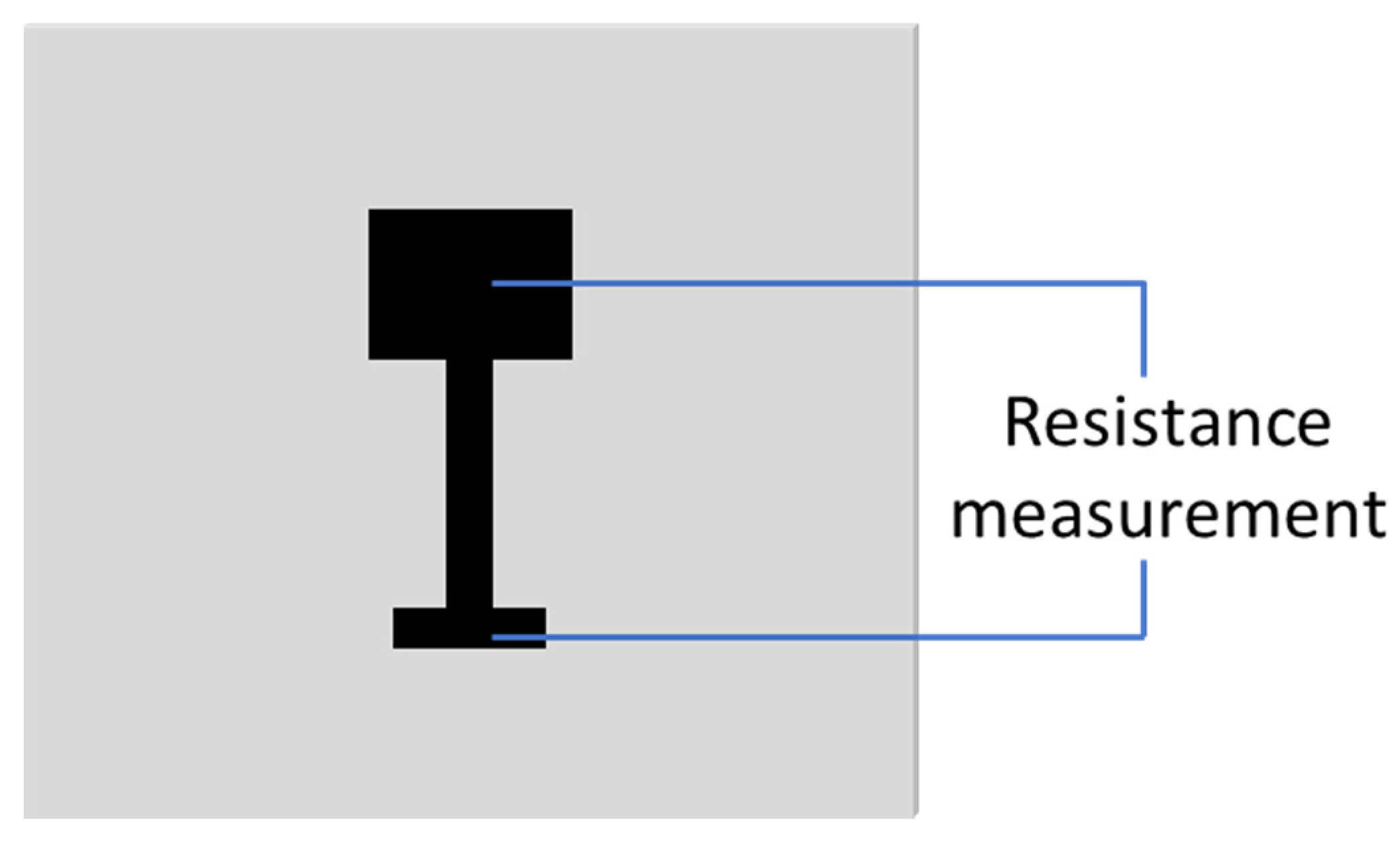
| Sample | Resistance (mΩ) |
|---|---|
| Original | 236 ± 1.8 |
| Treatment A | 230 ± 1.8 |
| Treatment B | 47 ± 6.9 |
| Silver film [38] | 45 |
| Atomic Concentration (%) | ||
|---|---|---|
| Sample | Original | After treatment B |
| O 1s | 18.3 ± 4.7 | 23.4 ± 2.7 |
| Ag 3d | 38.9 ± 1.8 | 1.0 ± 6.7 |
| C 1s | 41.2 ± 2.3 | 75.6 ± 0.8 |
| Cl 2p | 1.6 ± 18.5 | - |
| Atomic Concentration (%) | ||
|---|---|---|
| Sample | Original | After treatment B |
| C 1s 284.8 (C-C) | 42.3 ± 3.1 | 54.4 ± 1.2 |
| C 1s 286.3 (C-O) | 39.4 ± 3.1 | 32.8 ± 1.2 |
| C 1s 287.6 (C-Cl) | 9.2 ± 2.9 | - |
| C 1s 288.6(O-C=O/C=O) | 9.2 ± 2.8 | 12.8 ± 1.0 |
| Atomic Concentration (%) | |||
|---|---|---|---|
| O 1s | Ag 3d | C 1s | Cl 2p |
| 12.0 ± 13.1 | 39.5 ± 2.1 | 46.1 ± 1.9 | 2.4 ± 8.2 |
Publisher’s Note: MDPI stays neutral with regard to jurisdictional claims in published maps and institutional affiliations. |
© 2020 by the authors. Licensee MDPI, Basel, Switzerland. This article is an open access article distributed under the terms and conditions of the Creative Commons Attribution (CC BY) license (http://creativecommons.org/licenses/by/4.0/).
Share and Cite
Wang, B.; Zhang, H.; Choi, J.P.; Moon, S.K.; Lee, B.; Koo, J. A Post-Treatment Method to Enhance the Property of Aerosol Jet Printed Electric Circuit on 3D Printed Substrate. Materials 2020, 13, 5602. https://0-doi-org.brum.beds.ac.uk/10.3390/ma13245602
Wang B, Zhang H, Choi JP, Moon SK, Lee B, Koo J. A Post-Treatment Method to Enhance the Property of Aerosol Jet Printed Electric Circuit on 3D Printed Substrate. Materials. 2020; 13(24):5602. https://0-doi-org.brum.beds.ac.uk/10.3390/ma13245602
Chicago/Turabian StyleWang, Bing, Haining Zhang, Joon Phil Choi, Seung Ki Moon, Byunghoon Lee, and Jamyeong Koo. 2020. "A Post-Treatment Method to Enhance the Property of Aerosol Jet Printed Electric Circuit on 3D Printed Substrate" Materials 13, no. 24: 5602. https://0-doi-org.brum.beds.ac.uk/10.3390/ma13245602