1. Introduction
In the past few years, cadmium telluride (CdTe) solar cells have experienced a rapid performance improvement, with certified record power conversion efficiencies (PCEs) reaching 22.1% for cells and over 18.6% for modules [
1,
2]. Benefitting from its multi-advantages, including low manufacturing costs, a suitable bandgap, high light absorption coefficients, and, thus, a high theoretical efficiency of over 30% [
3], CdTe technology currently dominates the thin-film photovoltaic market. Despite the success in commercialization, it is still challenging to reproduce the record efficiency of CdTe solar cells in research institutes over the world. The efficiency loss is mainly caused by the low p-type conductivity and high electron affinity of CdTe films [
4,
5], which make them crucial challenges to form a good ohmic contact between CdTe and a metal electrode. The existence of non-ohmic contact produces a back barrier and increases the recombination at the interface of CdTe and the metal electrode, significantly limiting the open-circuit voltage (V
OC) and fill factor (FF) of CdTe solar cells. To overcome this issue, copper (Cu) is commonly used to improve the conductivity of CdTe and reduce the back-barrier height. However, the concern of long-time stability, due to the ease of Cu migration, inhibits its commercial applications [
6]. Group V element (e.g., As and P) doping, as an alternative to Cu doping for the desired long-time stability, has recently attracted intensive investigations. [
7,
8,
9] However, limited by the high capital costs of the equipment used for the in-situ doping and low effective doping level for the ex situ doping (due to aggregations at grain boundaries), group V doping has not been widely used by the researchers [
7,
10].
Copper thiocyanate (CuSCN), a low-cost and solution-processable material with a high work function of 5.3 eV [
11], has been widely used in dye-sensitized and organic-inorganic perovskite solar cells as the hole transport layer to facilitate the carrier extraction [
12,
13,
14]. In 2015, CuSCN was first reported by our group as copper source instead of metallic copper in CdTe solar cells, which delivers an impressive improvement in V
OC. [
11] Recently, CuSCN was successfully used in CdSeTe solar cells, showing an impressive V
OC of around 0.860 V and an efficiency of ~17.0%, which makes it a promising back-contact for CdTe solar cells [
15]. In this work, the application of solution processed CuSCN as the back contact in pure CdTe solar cells with zinc magnesium oxide (ZMO) as the buffer layer is investigated. ZMO is an emerging buffer layer in CdTe solar cells and helps boost their device performance, due to the reduction in interface recombination at the buffer layer/CdTe interface and parasitic light absorption by the buffer layer [
16]. Recently, PCEs of 19.1% and 18.6% for CdSeTe and pure CdTe solar cells, respectively, with ZMO buffer layers have been demonstrated [
17]. However, it has also been reported that an oxygen-free atmosphere is required for ZMO/CdTe devices during the CdTe deposition, as well as the post treatments; otherwise, the devices show poor performances, due to the presence of severe S-kinks [
18,
19]. Additionally, it is reported that the finished ZMO/CdTe devices degrade rapidly when exposing to the ambient atmosphere, likely due to the reaction between water and the ZMO film [
20]. All of these suggest that the post treatment of ZMO/CdTe solar cells should be done with great alertness.
Till now, there are only few reports on the optimization of post treatments, especially the back-contact treatment for ZMO/CdTe solar cells. During the optimization processes, we have tried different hole transport materials (e.g., metallic Cu [
21], carbon paste [
22]) and back surface treatments (e.g., hydroiodic (HI) solution [
23], Br methanol solution [
24] and MAI solution [
25] etching), which have been demonstrated effective in improving the CdS/CdTe device performance. However, most of these processes show adverse effects on the ZMO/CdTe devices, probably caused by the degradation of the ZMO films during the depositions or treatments. In this work, CuSCN dissolved in ammonium hydroxide solution (30 wt.% in water) was used to deposit CuSCN as a back contact for ZMO/CdTe solar cells. ZMO/CdTe devices with metallic Cu doping were used as a reference. Through the optimization of post annealing temperature and the CuSCN film thickness, the solar cells based on the ZMO/CdTe/CuSCN stack show a high PCE of 16.7%, with a V
OC of 0.857 V, a short-circuit current density (J
SC) of 26.2 mA/cm
2, and a FF of 74.0%. The result demonstrates that CuSCN is a robust hole transport material for CdTe solar cells with ZMO as the buffer layer.
2. Materials and Methods
The Schematic illustration of technological steps and investigation design in this work is shown in
Figure S1. The devices in this work were fabricated according to our previous report [
18]. Fluorine doped tin oxide coated glass (FTO, TEC12; Pilkington NA, Toledo, OH, USA) is used as the substrate after thermal ultrasonic cleaning in Micro-90 detergent (St. Louis, MO, USA) and deionized water at 70 °C. A 80 nm ZMO film was then deposited on the cleaned FTO glass, using a radio frequency sputter system at ambient temperature. The deposition was conducted at 6 mTorr pressure under a mix gas flow of 3% oxygen and 97% helium at a 25 W sputtering power, using a 2-inch ZMO target with 8 wt.% magnesium oxide. Then, a ~3.5 μm CdTe film was deposited in a close-space sublimation (CSS) chamber, with the source temperature of 560 °C, the substrate temperature of 495 °C, and a chamber pressure of 1 Torr. The CdCl
2 activation treatment was carried out by drop-casting a saturated CdCl
2 in methanol solution on the CdTe surface, followed with drying naturally and annealing at 420 °C for 20 min at 400 Torr with a 500 sccm helium gas flow. After cooling down, the CdTe film was rinsed by methanol thoroughly to clean the excess CdCl
2. The CuSCN solution was prepared by dissolving the CuSCN powder in ammonium hydroxide (30 wt.%), or diethyl sulfide with different concentrations (2 mg/mL and 10 mg/mL), and then stirring at room temperature for more than 5 h to facilitate the dissolution. Then, the solution was filtered using a 0.45 μm pore size PTFE filter for the later use. The thickness of CuSCN film was tuned by varying the spin coating speed (2000 rpm and 6000 rpm), and the solution concentration (2 mg/mL and 10 mg/mL). After the CuSCN deposition, the film was heated in our CSS chamber to different temperatures (140 °C, 160 °C, 180 °C) at a ramp rate of ~35 °C/min with a 500 sccm helium flow under ambient pressure. After cooling down naturally, a 40 nm of thick gold was deposited via a shadow mask with an individual area of 0.08 cm
2 in a thermal evaporator. The optimized reference ZMO/CdTe devices with evaporated Cu metal were fabricated in the same procedure, except evaporating a 3 nm Cu and 40 nm Au bilayer then annealing in ambient pressure at 200 °C for 20 min. The samples for the photoluminescence (PL) measurements were fabricated by depositing 2.5 μm CdTe films followed with the standard CdCl
2 treatment and the CuSCN or metallic Cu treatment, respectively. All the completed devices described above are listed in
Table 1.
The device bandgap diagram simulation was performed using the solar cell capacitance simulator (SACPS) [
26], and the parameters were used according to our previous publication [
18]. Steady-state photoluminescence (PL) measurement was performed utilizing a 532 nm continuous wave laser at ~5 W·cm
−2. Samples were excited through the film side. PL signal was detected by a symphony-II Si (CCD) detector (Horiba Scientific, NJ, USA) after a Horiba iHR320 monochromator (Horiba Scientific). The morphological microstructures of the CdTe films were characterized by a nanoscope atomic force microscope (Troy, MI, USA). The solar cell performance was characterized by measuring the current density-voltage (J-V) curves under AM1.5G illumination using a solar simulator (PV Measurements Inc. Point Roberts, WA, USA) and a source meter (Keithley 2400, Beaverton, OR USA). External quantum efficiency (EQE) spectra were performed on a QE system (PV Measurements, Beaverton, OR, USA). Temperature-dependent current-voltage (J-V-T) measurements were performed in a closed-cycle helium cryostat, with a tungsten lamp as a light source, and the temperature was varied from 200 to 310 K, with a step size of 10 K. An inhouse designed LabVIEW (National Instruments, Inc. Beaverton, OR, USA) control program was used to operate the temperature controller, and the Keithley 2400 source-meter for current and voltage data acquisition.
3. Results and Discussion
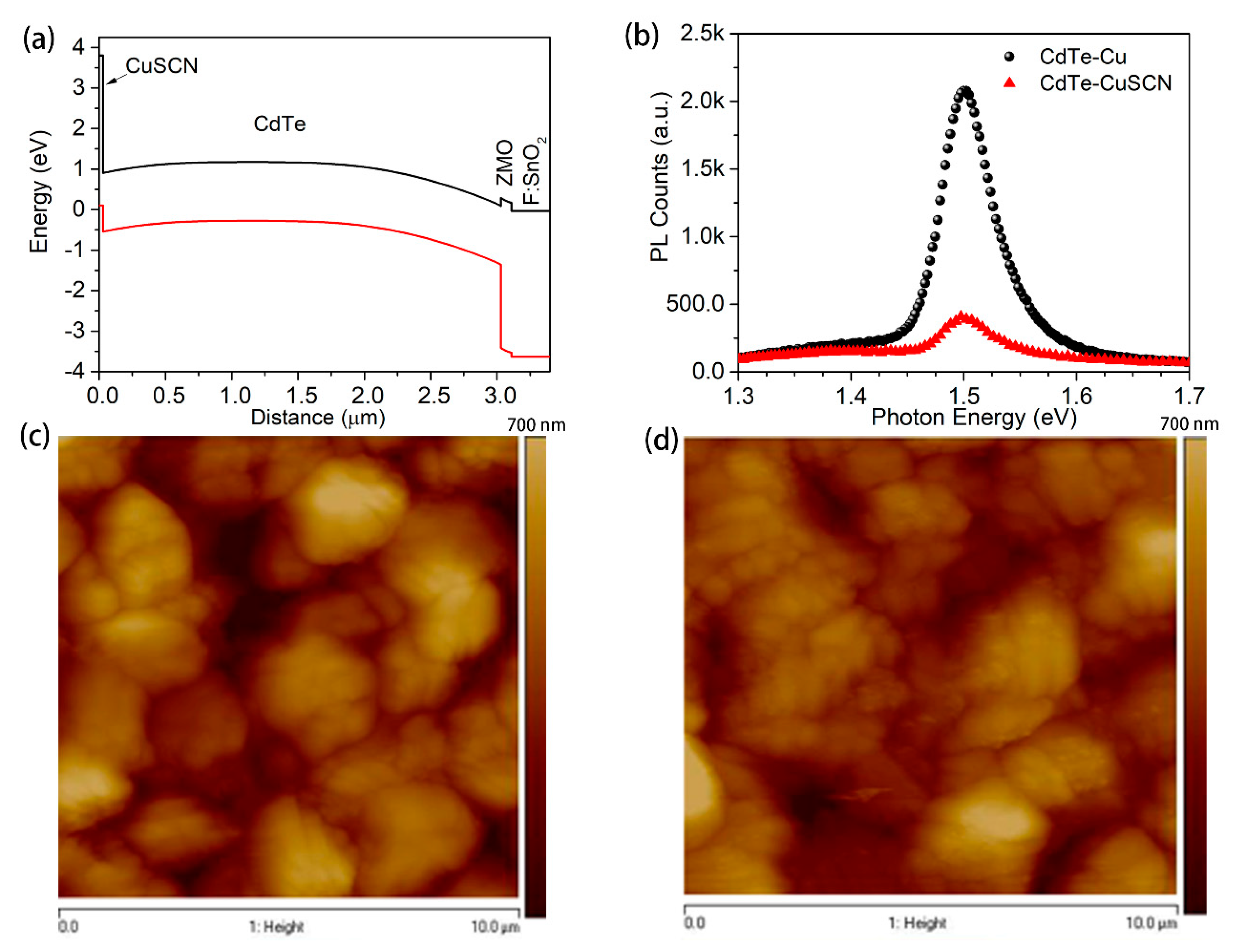
Figure 1a shows the simulated bandgap diagram of ZMO/CdTe solar cells, with CuSCN as the hole transport layer. The valence band offset between CdTe and CuSCN is favorable for the holes to be extracted from the CdTe layer. Additionally, the low electron affinity with respect to CdTe can favorably repel electrons and prevent them from diffusing into the back electrode. This CdTe/CuSCN heterostructure can eliminate the carrier recombination on the rear side of CdTe, consequently enhancing carrier collection efficiency. The steady-state PL was carried out to further confirm the carrier extraction efficiency (
Figure 1b). The CdTe-Cu reference sample exhibits a high intense PL emission peak, centered at 1.50 eV. With the presence of the CuSCN film, the PL emission peak shows pronounced intensity quenching, suggesting strong carrier extraction from the CdTe into the CuSCN. Atomic force microscopy (AFM) measurements were performed to confirm the uniformity of CuSCN film deposited on the CdTe films. The AFM image of bare CdTe film as shown in
Figure 1c, exhibits a uniform grain size of ~2 µm, with a root mean squared (RMS) roughness of 147 nm. With the spin-coated CuSCN layer (
Figure 1d), the RMS is slightly decreased to 139 nm, indicating a smooth coating of CuSCN particles.
The diffusion of Cu into the CdTe film is a necessary step to improve the ohmic contact between CdTe and the metal electrode. In CdTe/CuSCN stacks, the diffusion of Cu from CuSCN into CdTe not only increases the p-type conductivity of CdTe, but also leaves Cu vacancies in the CuSCN layer, which helps to further increase the work function of CuSCN [
27]. To optimize the CuSCN layer, the impact of the annealing temperature of CuSCN was investigated. As shown in
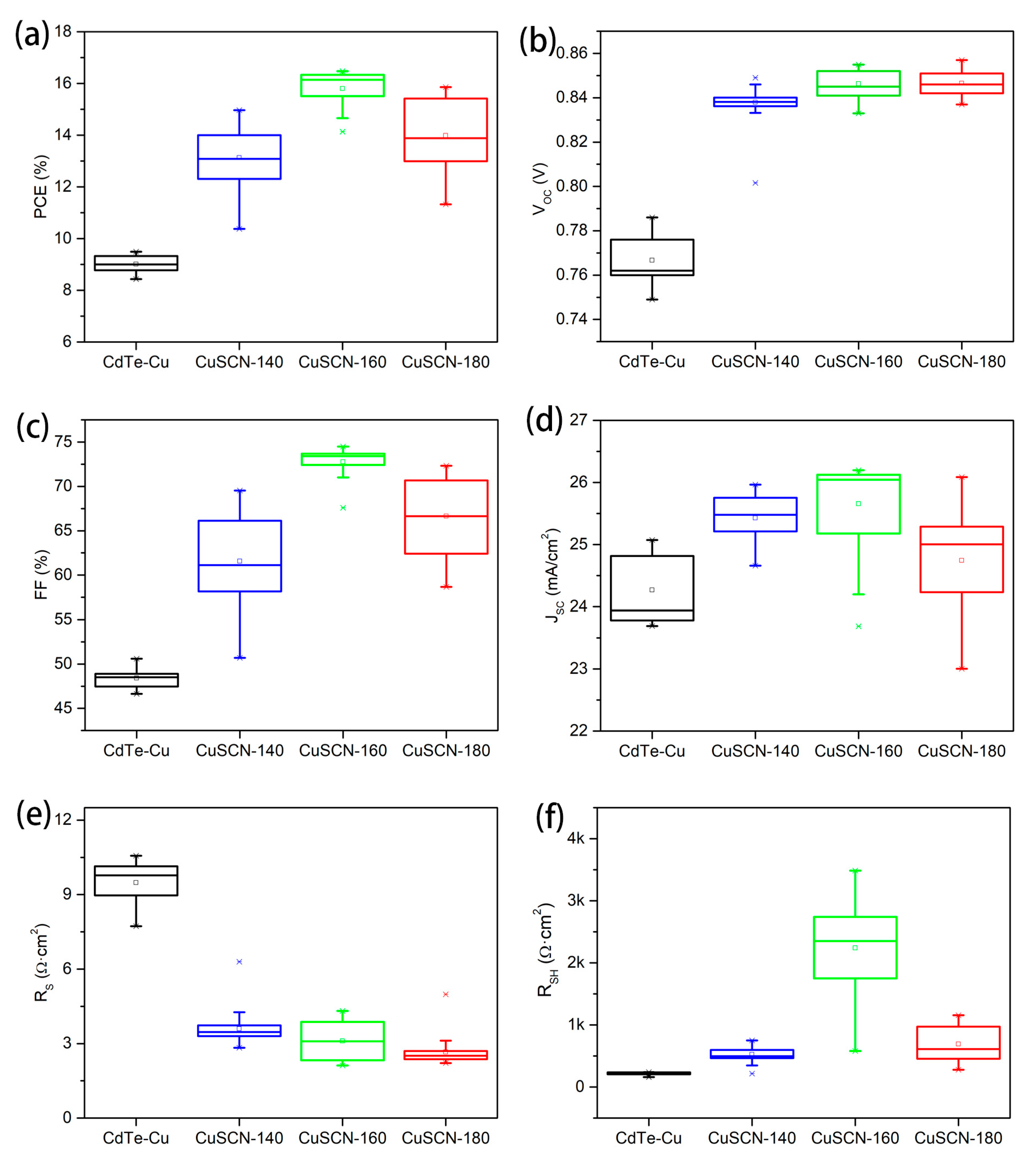
Figure 2, the ZMO/CdTe devices with the metallic Cu (named CdTe-Cu hereafter) was used as a control to compare with the ZMO/CdTe devices with a ~30 nm CuSCN layer. The devices with the CuSCN back contact were annealed at different temperatures (140 °C, 160 °C, and 180 °C, named CuSCN-140, CuSCN-160, and CuSCN-180, respectively). With the presence of CuSCN, the devices show overall higher performances than the control devices with the metallic Cu in all the PV parameters. The inferior performance of the reference devices is likely due to the over-diffusion of Cu through CdTe into the ZMO film, which significantly reduces the conductivity of ZMO film by several orders [
28,
29,
30]. We have tried to reduce the annealing temperature and time for the reference devices to reduce the diffusion length of Cu. However, the devices show even worse performances, probably due to the insufficient Cu diffusion. In comparison, CdTe-CuSCN devices annealed at 140 °C for a short duration (a few seconds) outperform the CdTe-Cu devices annealed at 200 °C for 20 min. This result indicates the possibility of reducing the adverse effect caused by the Cu over diffusion through performing Cu annealing at a lower temperature and a shorter holding time. Through lower temperature and shorter time annealing, the Cu diffused into CdTe can be easily confined on the rear side close to the back electrode. The predictable sharp copper concentration profile from the back surface to the bulk not only guarantees a proper Cu concentration on the rear side of CdTe to improve the ohmic contact, but also helps to reduce the Cu related deep trap states in the bulk and front interface caused by excess Cu concentrations [
31,
32,
33]. The proper Cu doping control through our CuSCN treatment can assist to enhance outstanding performance for the CdTe-CuSCN devices.
By increasing the annealing temperature, the mean VOC gradually increases from 0.838 V for CuSCN-140 to 0.847 V for CuSCN-180. The devices annealed at 160 °C deliver the best performance due to the largely improved FF (74.6%), compared to those devices annealed at lower or higher temperatures. This is mainly attributed to the higher hole concentration in CdTe bulk benefited from the proper copper diffusion. Higher hole concentration can boost a higher build-in potential (Vbi) and lead to less recombination in the depletion region and at the front interface, thereby resulting in larger FF, which can be further confirmed through the improvement of the shunt resistance (RSH). Accompanied with the variation of the annealing temperature, the RSH increases from the mean value 490 Ω cm2 for CuSCN-140 to 2360 Ω cm2 for CuSCN-160. When the annealing temperature is further increased to 180 °C, the mean RSH decreases to 610 Ω cm2, due to the excess Cu in the CdTe bulk and at the front interface. As the annealing temperature increases, the series resistance (RS) decreases slightly from 3.50 Ω cm2 in CuSCN-140 to 3.07 Ω cm2 in CuSCN-160, and further to 2.51 Ω cm2 in CuSCN-180. The JSC also shows similar trend as the FF and the shunt resistance at different annealing temperatures.
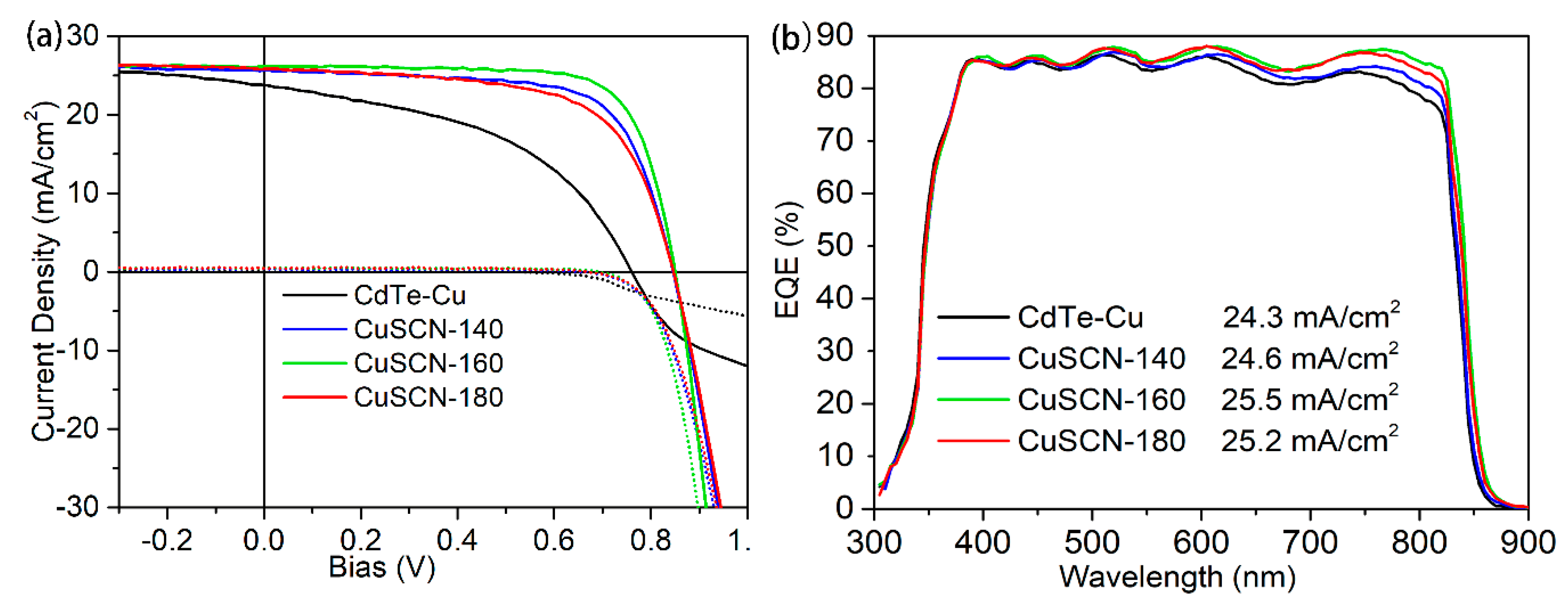
The J-V curves of the best cells of CdTe-Cu and CdTe-CuSCN are plotted in
Figure 3a, and more detailed parameters are displayed in
Table 2. Comparing to the CdTe-Cu device, the CdTe-CuSCN device shows a higher J
SC value, partially due to the reduced recombination at the depletion region and front interface as discussed above. Another reason is the reduced carrier recombination at the back interface between CdTe and the metal electrode, which can be confirmed by the absence of severe roll-over and cross-over effects in the J-V curves at high forward bias for the CdTe-CuSCN devices. The roll-over effect is commonly an indicator of insufficient copper doping on the rear side of CdTe film [
34,
35,
36], and the cross-over effect is due to photoconductivity in the buffer layer which could be caused by the aggregation of copper in the buffer layer. [
37] For this sake, the CdTe-Cu device delivers an efficiency of 9.49%, with V
OC of 0.786 V, J
SC of 24.8 mA/cm
2, and FF of 48.7%. In contrast, all the CdTe-CuSCN devices show the absence of the roll-over and cross-over effects at forward bias, indicating lower back-barrier heights, and less Cu aggregation at the front interface. Thus, the CdTe-CuSCN devices promise higher FF values (69.1% for the CuSCN-140, 74.0% for the CuSCN-160, and 71.4% for the CuSCN-180). Benefitting from the significantly improved FF, the CuSCN-160 device delivers the best efficiency of 16.5% with V
OC of 0.850 V, J
SC of 26.2 mA/cm
2 and FF of 74.0%. External quantum efficiency (EQE) curves were measured to examine the carrier extraction properties for all the devices. As shown in
Figure 3b, all the devices show the overlapped curves in short wavelength below 400 nm due to the parasitic absorption of ZMO films. Between 500 to 800 nm, the CdTe-Cu shows the lowest quantum efficiency, compared to the CuSCN ones. The deviation enlarged gradually as the wavelength increases, indicating a larger difference in the recombination properties at the CdTe and metal electrode interface. This can be attributed to two primary reasons: one is that the larger back-barrier height in CdTe-Cu for the hole extraction, and the other one is that the high conduction band offset between CdTe and CuSCN, which can reflect the unfavorable electron diffusion into the CuSCN layer, and thereby suppress the recombination at the back interface. This is consistent with the result of PL quenching for the CdTe/CuSCN film stack. For the CdTe-CuSCN devices annealed at various temperatures, the variation in the quantum efficiency is mainly located at the long wavelengths, probably due to the difference in the Cu concentration at the back surface of CdTe. At higher temperatures, more Cu in the CuSCN layer can diffuse into CdTe. The CuSCN-160 device shows the highest quantum efficiency at long wavelengths, indicating the lowest back barrier height, which can be further confirmed in the temperature dependent J-V measurement, described in the later section. When the annealing temperature is further increased to 180 °C, the Cu concentration at back side is too high, and the interstitial compensation defects Cu
i, instead of substitutional acceptor defects Cu
Cd become dominant, and the back barrier height increases, causing lower quantum efficiencies at long wavelengths for CuSCN-180. Overall, the CuSCN-160 device delivers the highest integrated current density of 25.5 mA/cm
2, with quantum efficiency over 85% in the whole wavelength range, and the highest value of 88.0% at 605 nm, showing decent carrier transport and extraction properties.
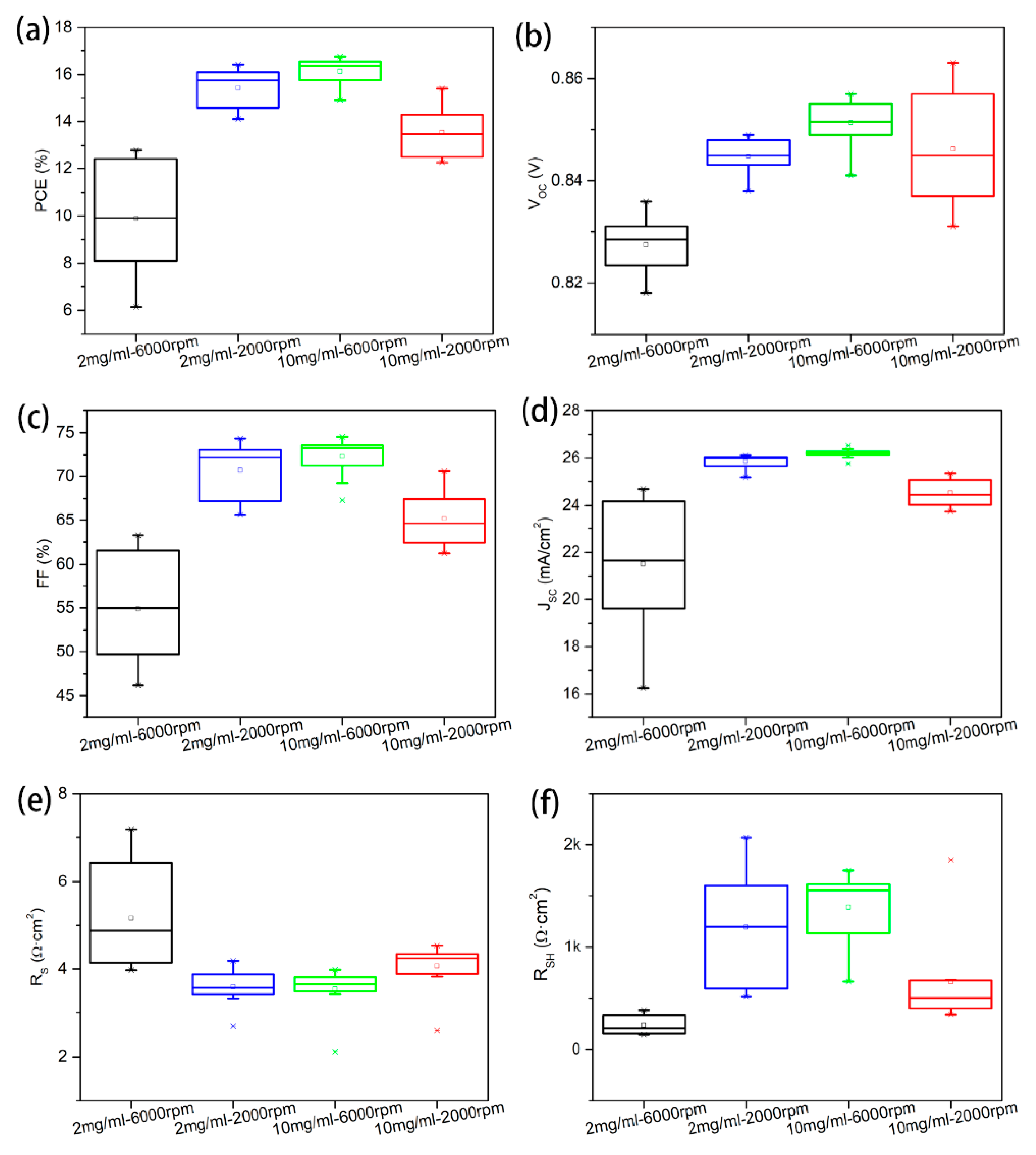
Due to the high resistivity of CuSCN, the thickness of CuSCN layer is critical for better carrier extraction efficiency. CdTe devices with different CuSCN thicknesses are fabricated using CuSCN solutions with different concentrations (2 and 10 mg/mL) and spin-coating speeds (2000 and 6000 rpm), which are named 2 mg/mL-6000 rpm, 2 mg/mL-2000 rpm, 10 mg/mL-6000 rpm, and 10 mg/mL-2000 rpm, respectively. We tried to measure the CuSCN film thicknesses with different deposition parameters through scanning electron microscopy (SEM) measurements. Unfortunately, the CuSCN films are too thin (less than 30 nm) to be accurately measured through SEM images. The cross-sectional SEM images of the whole devices with the thickest CuSCN film deposited at 2000 rpm using 10 mg/mL CuSCN solution were shown in
Figure S2, from which we can know the CuSCN film thickness is about 30 nm, and the others should be thinner than 30 nm. Based on spin-coating features, the thickness of the CuSCN films should rank as 2 mg/mL-6000 rpm < 2 mg/mL-2000 rpm < 10 mg/mL-6000 rpm < 10 mg/mL-2000 rpm, which can be further confirmed by the gradual change of device performance. As shown in
Figure 4, the V
OC increases gradually as the thickness of CuSCN increases. This can be attributed to the increase of CuSCN film thickness, which supplies more Cu for the diffusion during the annealing treatment, thus, a higher carrier concentration in the CdTe film and higher V
OC is generated. The complement of Cu doping concentration also helps to improve all the other J-V parameters, including higher FF, J
SC, R
SH, and lower R
S, yielding a highest efficiency 16.7%, with V
OC of 0.857 V, J
SC of 26.2 mA/cm
2, and FF of 74.5%. The detailed information of the best cells with different CuSCN thicknesses are shown in
Table 3, and the corresponding J-V curves are shown in
Figure S3. As the thickness of CuSCN film increases, PCEs increases from 12.8% to 16.7%. This improvement can be assigned to two major reasons: first, suggested by significant improvement in FF, the CuSCN film became more uniform and the CdTe film can be fully covered by CuSCN film; second, the Cu concentration in CdTe increases gradually due to the increase of CuSCN film thickness, and thus, higher V
OC values can be obtained. When the CuSCN film thickness is further increased by spin-coating a 10 mg/mL CuSCN solution at 2000 rpm, V
OC is further increased to over 0.863 V, but all the other parameters decrease with a J
SC to 25.3 mA/cm
2, a FF to 70.1%, yielding an efficiency to 15.4%. This is likely ascribed to the high resistance of CuSCN film because, taking an example of the same 10 mg/mL CuSCN solution, decreasing the spin speed from 6000 rpm to 2000 rpm results in increased R
S from 3.43 to 4.17 Ω cm
2.
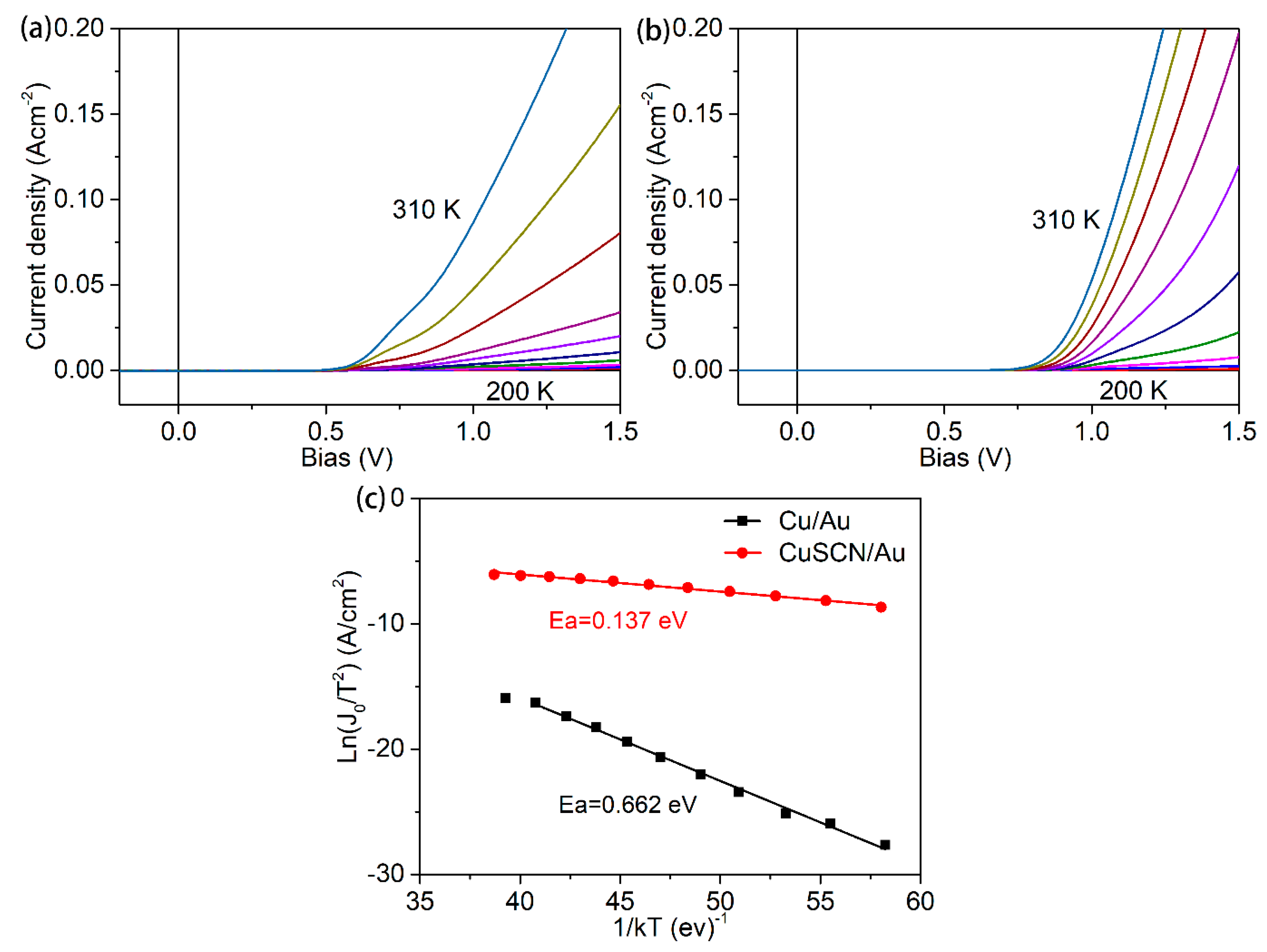
In order to investigate the origin of device performance improvement with the CuSCN as back contact, the temperature-dependent dark J-V measurements for devices with copper metal (CdTe-Cu) and CuSCN (CuSCN-160) as the back contact were carried out at temperatures ranging from 200 to 310 K, to quantify the back-barrier height as shown in (
Figure 5a,b). The temperature dependent dark J-V measurements, as shown in
Figure 5a, b, were carried out at temperatures ranging from 200 to 310 K to quantify the back-barrier heights of the devices, with Cu metal and CuSCN as the back contact. For the CdTe-Cu device, the J-V curves show a severe roll-over effect at a high forward bias at room temperature, and the roll-over becomes more pronounced as the temperature decreases to 200 K. In contrast, the CdTe-CuSCN device shows a typical diode behavior, without roll-over in the temperature range of 310 to 250 K. The presence of roll-over effect indicates the existence of a back barrier at the back interface and thereby enhanced carrier recombination. The values of the back-barrier height for the CdTe-Cu and CdTe-CuSCN are calculated according the reference. [
38] As shown in
Figure 5c, the CdTe-Cu device exhibits a back-barrier height of 0.662 eV, which is extremely high to extract the holes efficiently from the CdTe to the metal electrode. This further explains the origin of low device performances with efficiencies lower than 10%. The CuSCN-160 device possesses a 0.137 eV back-barrier height, which is much lower than that of the CdTe-Cu devices. This small back-barrier height in CuSCN-160 boosts higher carrier extraction efficiency, explaining the origin of the distinctive EQE curves shown in
Figure 3b.
Through the careful optimization of the CuSCN treatment, depositing CuSCN film using ammonium hydroxide with water as the solvent was demonstrated to be an efficient means of improving the device performances. However, it has been reported that the performance of ZMO/CdTe device degraded gradually while being exposed to ambient conditions, due to the reaction between water in atmosphere and MgO in ZMO films. [
19] To further confirm whether the water in the CuSCN solution will degrade the performance of the ZMO/CdTe solar cells during the annealing treatment, a CuSCN solution without water was used for the CuSCN film deposition. Diethyl sulfide has been widely used as the solvent of CuSCN for hole transport layer deposition. [
39,
40] For the fabrication of the CdTe-CuSCN device with Diethyl sulfide as solvent, the same procedures used for the CuSCN treatment were used. As shown in
Figure S4, the devices using CuSCN in ammonium hydroxide show slightly higher and more uniform performances than those using diethyl sulfide as the solvent. This is because that the uniformity of the CuSCN film deposited using ammonium hydroxide solvent is much better than that using diethyl sulfide as the solvent, which has been confirmed in our previous report [
15]. These results further confirm that the performance of our ZMO/CdTe devices is not affected by the water in ammonium hydroxide, demonstrating a robust hole transport layer deposition procedure for ZMO/CdTe solar cells.

 ,
, 


