Article

Synthesis and Characterization of Al- and SnO2-Doped ZnO Thermoelectric Thin Films

1
College of Engineering, Shibaura Institute of Technology, 307 Fukasaku, Minuma-ku, Saitama 337-8570, Saitama Prefecture, Japan
2
Toyota Technological Institute, Tempaku Ward, Hisakata 2-12-1, Nagoya 468-8511, Aichi Prefecture, Japan
3
Physics and Engineering Department, Dillard University, 2601 Gentilly Blvd, New Orleans, LA 70122, USA
4
SSS Optical Technologies, 515 Sparkman Drive, Huntsville, AL 35816, USA
5
Muroran Institute of Technology, 27-1 Mizumotocho, Muroran 050-8585, Hokkaido Prefecture, Japan
6
International Center for Materials Nanoarchitectonics (WPI-MANA), National Institute for Materials Science (NIMS), Namiki 1-1, Tsukuba 305-0044, Ibaraki Prefecture, Japan
7
Graduate School of Pure and Applied Sciences, University of Tsukuba, 1-1-1 Tennodai, Tsukuba 305-8577, Ibaraki Prefecture, Japan
8
Central Research Institute of Electric Power Industry (CRIEPI), 2-6-1 Nagasaka, Yokosuka 240-0196, Kanagawa Prefecture, Japan
*
Authors to whom correspondence should be addressed.
Submission received: 8 October 2021 / Revised: 6 November 2021 / Accepted: 10 November 2021 / Published: 16 November 2021

Abstract

:
The effect of SnO2 addition (0, 1, 2, 4 wt.%) on thermoelectric properties of c-axis oriented Al-doped ZnO thin films (AZO) fabricated by pulsed laser deposition on silica and Al2O3 substrates was investigated. The best thermoelectric performance was obtained on the AZO + 2% SnO2 thin film grown on silica, with a power factor (PF) of 211.8 μW/m·K2 at 573 K and a room-temperature (300 K) thermal conductivity of 8.56 W/m·K. PF was of the same order of magnitude as the value reported for typical AZO bulk material at the same measurement conditions (340 μW/m·K2) while thermal conductivity κ was reduced about four times.

1. Introduction

The increasing worldwide demand for energy and the resultant depletion of fossil fuels have brought new challenges for the scientific community [1]. One of the major issues is to develop high-efficiency devices for capturing energy from abundant natural sources such as solar, wind and geothermal energy. Another surplus, but mostly unused, source of energy is wasted heat. There are huge waste heat sources in our environments covering a wide range of temperatures (300~1200 K): industrial processes, domestic stoves and radiators, electrical lighting, pipelines, electrical substations, subway networks, automotive exhaust tubes, but also geothermal heat, body heat, and so on: about 66% of the annual world energy consumption is lost as waste heat, and the loss corresponds to the stellar amount of 3·1020 J per year, just considering the past 10 years [2,3]. A highly promising method for energy recovery from such heat sources is the utilization of thermoelectric (TE) materials that can convert various types of waste heat flow into electricity. The possibility of conversion of heat in electricity was discovered in 1821 by Thomas Seebeck [4]: a junction of two metals generates the thermoelectric voltage ΔV when a temperature gradient ΔT is created across it. In mathematical form it can be expressed as:
ΔV = S · ΔT
where S is the material-dependent Seebeck coefficient. The performance of any TE material is quantified by the figure of merit (ZT):
Z T = σ S 2 κ e l + κ p h T
where σ is the electrical conductivity, S the Seebeck coefficient, T the absolute temperature, κel the electrical thermal conductivity and κph the phononic thermal conductivity being κ = κel + κph the total thermal conductivity.
ZT is related to the efficiency η of heat/electrical energy conversion by the relation:
η = T T H 1 + Z T a v e 1 1 + Z T a v e + T C T H
State-of-the-art TE materials for heat conversion can operate at T = 300~1200 K, with ZT = 0.1~2.6, corresponding to η = 1~20%. Therefore, after two centuries, TE devices are seldom utilized in daily life. TE modules have obtained brilliant success, however, in niche applications, for example for powering the space probe Cassini [5], while high-conversion modules to harvest waste heat of car engines remained at the state of prototypes [6]. ZT and η must be strongly improved to make TE power competitive with the common thermodynamic cycles based on fossil fuel burning, solar conversion and nuclear power plants. The improvement of ZT can be obtained by enhancing σ and/or S, or the product σS2 which is called “power factor” (PF), and/or by decreasing the total thermal conductivity. However, κel = LTσ, with L = 2.44 × 10⁻⁸ W·Ω·K−2 is the Lorentz number while κph = 1/3 CvЛ where C is the heat capacity, v is the speed of phonons, Л is the phonon mean free path. It is thus necessary to decouple σ and κel and work on the depression of κph.
Since the discovery of the Seebeck effect, the benefit of TE harvesting has been understood and a wealth of TE materials has been discovered. After the discovery of BiTe with ZT = 0.5 [7] in 1954, the ZT of TE materials did not improve for a very long time. In 1993, a seminal paper [8] theoretically predicted the drastic depression of κph due to reduction of the mean free path of phonons (Л) to a few nanometers, which resulted in substantial improvement of ZT. This concept was firstly validated in Bi2Te3/Sb2Te3 multilayer thin films incorporating natural nano-sized precipitates, showing the extremely small κ value (0.22 W·m−1 K−1) and a huge value of ZT = 2.5 at T = 300 K [9].
These results were due to the scattering of phonons by nano-defects spontaneously formed inside the thin films. However, TE harvesters based on BiTe and related materials cannot be produced on a large scale because they contain rare (Te) and poisonous (Sb, Bi, Pb) elements, and require high-cost processing. Though the last ten years a great progress has been made with ZT = 2.6 for SnSe single crystals [10] and 3.1 for polycrystalline SnSe [11], there is still room for finding even more efficient TE materials in a wide T region.
In particular, the attention of researchers has been focused on the development of stable, environmentally benign, abundant, and cost-effective TE materials based on oxides. In the 1990s, extensive research in the area of bulk oxides focused on the enhancement of the TE performance using atomic substitutions and improved grain connection [12,13,14,15]. To date, the best TE performance of the currently available oxide materials is ZT = 0.64 for n-type Zn0.96Al0.02Ga0.02O [13] and 0.74 for p-type Ca2.5Tb0.5Co4O9 [14] at 1000 K. The ZT of oxides is not yet up to the level of the best conventional TE materials and needs to be drastically improved to be acceptable for practical applications. The bulk oxides also have the main disadvantages of requiring a long time for sintering and fabrication of the n- and p- elements and their assembly in modular shape, and mechanical fragility. All these drawbacks can be overcome by using oxide thin films. Thin-films have significant advantages, such as low dimensionality, rapid fabrication, control of strain at the interface with substrates, and the possibility to insert artificial nano-defects to improve the phonon scattering. Thermoelectric thin films are also attractive for their applicative potential for energy harvesting to power Internet of Things (IoT) sensors [15,16].
Recently, our group studied oxide-thin TE films and obtained encouraging preliminary results. First, epitaxial thin films of 2% Al-doped ZnO (AZO) were fabricated by pulsed laser deposition (PLD) on several single crystal (SrTiO3, Al2O3) and amorphous (silica) substrates. Regardless of a particular substrate, the films always showed higher values of ZT in comparison with the corresponding bulk AZO: for example, at T = 600 K, ZTAZO-on-STO = 0.03 while ZTbulk = 0.014 [17,18]. The superior performance of films is due to their lower thermal conductivity: κAZO-on-STO (300 K) = 6.5 W/m·K [16,17] while κbulk (300 K) = 34 W/m·K. In these series, the grain boundaries can be considered as natural nanodefects for an enhanced scattering of phonons and consequent decrease of κ. As a demonstration of this effect, the film on fused silica, showing additional grain boundaries at the seed layer on the substrate, had even lower thermal conductivity: κsilica (300 K) = 4.89 W/m·K and larger ZT: ZTsilica (600 K) = 0.045 [18].
The insertion of artificial nanodefects has been subsequently considered with the purpose of further reduction of κ and enhancing ZT. Several approaches have been tried by our group: insertion of hydroquinone nanolayers in AZO films prepared by atomic layer deposition (ALD): κALD (300 K) = 3.56 W/m·K [19]; addition of polymethylmethacrylate (PMMA) particles to AZO films prepared by multi-beam multi-target matrix-assisted PLD (MBMT/MAPLE-PLD): κMAPLE (300 K) = 5.9 W/m·K and ZTMAPLE (600 K) = 0.0061 [20]; formation of nanopores in AZO films prepared by mist-chemical vapor deposition (mist-CVD): κporous (300 K) = 0.60 W/m·K and ZTporous (300 K) = 0.057 [21]; dispersion of Al2O3 nanoparticulate in AZO films prepared by surface-modified target PLD: κnanoAl2O3 (300 K) = 3.98 W/m·K and ZTnanoAl2O3 (600 K) = 0.0007 [22]. Several groups worldwide have recently obtained excellent results with different kinds of dopant, like the κ (300 K) = 1.19 W/m·K and ZT (300 K) = 0.1 of magnetron sputtered AZO films by Loureiro et al. [23], κ (323 K) = 3.37 W/m·K and ZT (423 K) = 0.052 of CNT-added evaporated porous AZO films by Liu et al. [24], the κ (300 K) = 1.1 W/m·K and ZT (300 K) = 0.042 of amorphous ZnOxNy PLD films by Hirose et al. [25], the κ (300 K) = 1.8 W/m·K and ZT (383 K) = 0.019 of dual-doped AlGaZnO PLD films by Nguyen, et al. [26], just to cite the most impressive. All these successful examples highlight the promise of nanostructured doped ZnO films for future energy-harvesting applications.
In this work, we have focused on enhancing the thermoelectric performance of Al-doped ZnO films by the addition of a controlled amount of SnO2 as a secondary dopant. AZO has the same structure of hexagonal ZnO: wurtzite, hexagonal, space group P63mc, cell parameters a = b = 0.3289 nm and c = 0.5307 nm, while SnO2 is cassiterite, tetragonal, space group P42/mnm with cell parameters a = b = 0.4832 nm and c = 0.3243 nm. Since the mismatch between the a-axis of AZO and the c-axis of SnO2 is 1.4%, we forecasted the growth of quasi-epitaxial nanostructures (nanoparticles) of SnO2 with cSnO2//aAZO, dispersed in the AZO matrix.
The motivation of this work is to prove the presence of SnO2 nanoparticulates in the AZO matrix and verify the optimal content of SnO2 for the TE properties of the nanocomposite Al- and SnO2-doped (AZO + SnO2) thin films.

2. Materials and Methods

Two sets of four thin films were prepared using various compositions and substrate materials. All samples were deposited both on amorphous silica and c-axis oriented alumina by pulsed laser deposition (PLD) technique focusing a Nd:YAG (266 nm, 10 Hz) laser on dense pellets. Four commercial targets (Kurt Lesker Ltd., Jefferson Hills, PA, USA) used for film making had different contents of SnO2 (0, 1, 2 and 4 wt.%) dispersed in the Al-ZnO (AZO) main phase where the Al content was kept as 2 wt.%. Prior to the deposition, the substrates were cleaned at 773 K for 2 h, then glued by conductive silver glue to a rectangular Inconel plate, which was put in direct thermal contact with a cartridge heater and finally inserted into the vacuum chamber. All films were grown with an energy density of about 4.2 J/cm2 for 60 min at 573 K, in the atmosphere of 20 mtorr of oxygen. The samples deposited on silica are named AZO_xS and the ones deposited on alumina AZO_xA, with x = 0, 1, 2 and 4 referring to the concentration (wt.%) of the SnO2 in the respective targets.
Electrical conductivity (σ) and Seebeck coefficient (S) were measured by means of the four-probe method using a ZEM-3 (ULVAC Advance-Riko, Yokohama, Kanagawa, Japan) apparatus under partial He pressure to assure thermal transport between the heater and the sample. Measurements with ZEM-3 were conducted performing three cycles between 353 and 573 K and measuring both heating and cooling processes. The σ and S curves reported in Section 3.2 for each sample were those obtained from the last cooling cycle, considered as the most stable and reliable. The uncertainties of the ZEM-3 measurements were ±4% for the electrical conductivity and ±3% for the Seebeck coefficient.
For comparison and validation of data, some selected samples were also characterized by a custom-made apparatus whose working principle and measurement protocol are reported elsewhere [27,28]. The error in the thermoelectric coefficients measurements is ±5% in the case of σ, and ±7% for S.
The thickness of the thin films (in the range 295–585 nm, as summarized in Table 1) was measured using a Dektak 6M Stylus Profiler (Bruker, Billerica, MA, USA) and a Filmetrics Profilm 3D (KLA, Milpitas, CA, USA).
The X-ray diffraction analysis was conducted using a Bragg-Brentano powder diffractometer (Smart Lab 3, Rigaku Corporation, Tokyo, Japan) using the Cu Kα radiation in the 10–100° angular range with an angular step of 0.02° (power settings: 40 mA, 40 kV).
The TEM images and EDS analysis were conducted using a JEM-2100F (JEOL, Akishima, Tokyo, Japan) with EDS spectroscopy. The STEM beam size was set to 0.5 nm.
The picosecond time-domain thermo-reflectance (TD-TR) technique using a customized system PicoTR (PicoTherm, Netzsch Japan KK, Tsukuba, Japan) was utilized to measure the thermal conductivity of the samples at room temperature (T = 300 K) in the cross-plane direction.
Measurement of Hall coefficient at room temperature was performed using a standard four-terminal method with a commercial PPMS instrument (Quantum Design, San Diego, CA, USA) at an AC current of 5 mA.

3. Results and Discussion

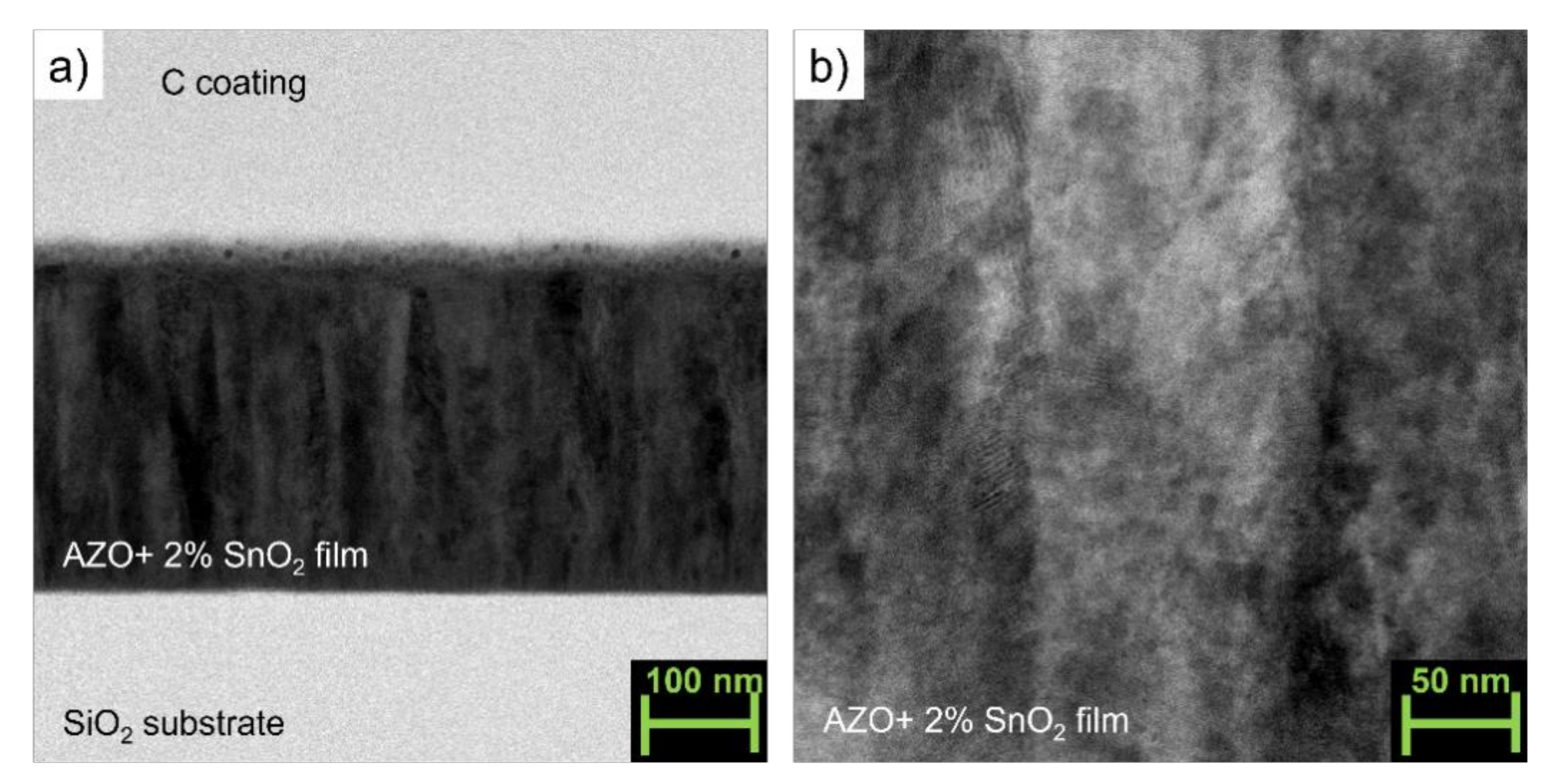
3.1. Structural and Morphological Characterization

The XRD spectra of the thin films fabricated on amorphous silica and single-crystal c-axis oriented Al2O3 are presented in Figure 1a,b, respectively.
On both substrates, the preferred orientation of AZO films was along the c-axis since only (00l) reflection appeared. The presence of SnO2 in the films of both series was undetectable by X-rays even for the highest amount (x = 4).
The cross-sectional TEM images (magnification 150,000, Figure 2a and Figure 3a of two representative samples deposited on fused silica without (AZO_0S) and with the addition of SnO2 (2 wt.%, AZO_2S) reveal a typical columnar growth along the c-axis of the films as often reported in the literature for AZO PLD thin films [16,17,19,21]. The addition of SnO2 (AZO_2S) did not affect the morphology of the films. The higher magnification images (300,000×, Figure 2b and Figure 3b for AZO_0S and AZO_2S, respectively) show that the columns were well connected without the presence of pores or misoriented grains so that the density of the films could be considered close to the theoretical value.
The TEM-EDS mapping performed on the sample AZO_2S (Figure 4) reveals a uniform distribution not only of the elements Al, Zn, O, but also of Sn. Contrary to the predictions based on the 1.4% lattice mismatch, Sn did not form nanoscale aggregates in the AZO matrix, but presumably entered as substitutional or interstitial atoms in the AZO elementary cell. According with TEM-EDS analysis, the atomic percentage of Sn in the film prepared with 2 wt.% SnO2-added AZO target is 0.49%. The atom % of oxygen is 33.91%. Since it is not possible to separate the contribution of oxygen from SnO2 and from ZnO, we can only compare the percentage of Sn in the target and in the film. The percentage of Sn in SnO2 is 78.77%, which in 2 wt.% SnO2 corresponds to 1.58%. This means that in the film the amount of Sn is about 1/3 than in the target. Si is not considered in the discussion being part of the substrate only.

3.2. Transport and Thermoelectric Characterization

Room temperature Hall measurement was taken to find the carriers’ concentration nH and mobility μH values for the AZO_xS and AZO_xA films. The results are in Figure 5, together with room temperature resistivity values from the ZEM-3 analysis.
The resistivity at room temperature has a clear ascending trend with the increase of the content of SnO2 for both substrates. The films on Al2O3 had half the resistivity of those on silica. The range of nH was almost the same for two substrates, and of the order of 1020 cm−3, as expected for a typical semiconductor such as AZO. The maximum number of carriers occurred at x = 1 on silica and at x = 2 on Al2O3. The carrier mobility had the maximum at x = 2 on both substrates but was about 20 times larger for AZO_2A than for AZO_2S. AZO_0S had greater mobility than AZO_0A and this could be explained by the larger misfit dislocations generated on Al2O3, due to a lattice misfit of 15% [18,29]. Surprisingly, by increasing the content of SnO2 doping, there was a reversal trend and the films grown on Al2O3 presented higher mobility, with the maximum value for AZO_2A-20 times larger than for AZO_0S.
The electrical conductivity (σ) for the AZO films is presented in Figure 6 as a function of temperature in the range 300–600 K. Figure 6 shows that σ increases with rising temperature, confirming the semiconductor behaviour of the samples. On both substrates, the film grown without additional SnO2 had the largest σ followed by the film with x = 2.
The temperature dependence (300–600 K) of Seebeck coefficient (S) of the AZO films is plotted in Figure 7. S had a negative sign, confirming the n-type conductivity of AZO. Figure 7 shows that S decreases with the rising temperature, a reversal trend with respect to σ as commonly expected for semiconductor materials. On both substrates, the pure AZO film had the lowest S while the sample fabricated with a target containing 4% of SnO2 presents the largest one.
The Seebeck coefficient can be expressed as [30]:
S = 8 π 2 k B 2 3 e h 2 m T 3 n 2 / 3
where kB is Boltzmann’s constant, h is Planck’s constant, T is the absolute temperature, m* is the effective mass and n is the carrier concentration. The effective mass is also expressed as m* = α me, where me is the mass of the electron and α is a positive rational number.
The room temperature (300 K) “Pisarenko plots” (S versus nH) for both series of films are presented in Figure 8. According to the graphs, m* was (0.3–0.6) me and (0.2–0.7) me for the films grown on silica and alumina, respectively. The fractional me was consistent with the parabolic band approximation and relatively simple band structure reported for ZnO [31].
The calculated power factor (PF) as a function of temperature is shown in Figure 9. The maximum power factor value was found for sample AZO_2S at 573K as 211.78 mW/m·K2. This value was of the same order of magnitude as that measured for bulk AZO at the same conditions (−340 mW/m·K2) [32] and was also comparable with the values reported for AZO thin films [17,18,23,24,25,26].
The PFs of all films at 353 K and 573 K are summarized in Figure 10, making clear that on both substrates, 2% of SnO2 represents the optimal dopant concentration.
For the films AZO_0S and AZO_2S deposited on silica the measurements were repeated using two different apparatuses to verify the accuracy of the reproducibility of data. The comparison between the pair sets of data for σ, S and PF is reported in Appendix C.
The transport and thermoelectric properties of the films are summarized in Table 1.
The room temperature (300 K) thermal conductivity (κ) of the sample with the highest PF (AZO_2S) and of a reference sample from the same batch (AZO_0S) was evaluated by the TD-TR method [32,33,34,35] according to the details described in Appendix A. The value of κ was 8.88 and 8.56 W/m·K for samples AZO_0S and AZO_2S, respectively. These values were in the same range as those reported for pure AZO films deposited by PLD [16,17,21]. Therefore, the four-fold decrease of κ with respect to bulk [32] must be attributed to the phonon scattering of grain boundaries, and not to the addition of SnO2. The calculation of ZT (T = 353 K) using Equation (2) gave the following result: ZT (AZO_0S) = 0.003 and ZT (AZO_2S) = 0.004, of the same order as for AZO thin film deposited by PLD on different substrates. Conservative estimates of ZT′ (T′ = 573 K) were ZT′ (AZO_0S) = 0.009 and ZT′ (AZO_2S) = 0.014. Since for oxide thin films κ is expected to decrease with T [33], ZT was calculated using a conservative approach from the PF values at 353 K or 573 K, κ at 300 K, and T = 353 K or 573 K.
These values of ZT did not surpass the reported performance of bulk AZO at the same conditions and were also of the same or lower level as for other AZO films prepared by PLD. This indicated that SnO2 could not be considered as an optimal dopant for AZO thin films for thermoelectric applications. On the other hand, it could be that the fine dispersion of SnO2 into AZO matrix enhanced the photoelectric response of AZO, as reported for SnO2/ZnO hierarchical nanostructures prepared by the electrospinning method [34], or could be used to fabricate compact gas sensors, as reported for ZnO–SnO2 nanofibers [35].

4. Summary

In summary, we fabricated using pulsed laser deposition (PLD) two series of thermoelectric thin films of Al-doped ZnO (AZO) doped with various concentrations of SnO2 (x = 0, 1, 2, 4 wt.%) on the substrates made of fused silica and Al2O3 (001) single crystals. The goal was to enhance the thermoelectric performance. All the films were c-axis oriented. The films deposited on silica showed the highest values of Seebeck coefficient (S) and power factor (PF) in comparison with the films on Al2O3 with the same content of SnO2. The AZO film on silica with x = 2 showed the best performance, with σ = 385.0 S/cm, S = –74.17 mV/K, and PF = 211.8 μW/m·K2 at the maximum operating temperature (573 K). The room temperature (300 K) thermal conductivity of this sample was evaluated as κ = 8.56 W/m·K, with a calculated figure of merit ZT (353 K) = 0.003 and a projected value of ZT (573 K) = 0.014, comparable with ZT of the nanostructured PLD AZO films grown on several substrates.

Author Contributions

Conceptualization, P.M. and G.L.; Data curation, G.L. and S.S. (Saurabh Singh); formal analysis, G.L.; funding acquisition, T.M. and A.D.; investigation, G.L., S.S. (Saurabh Singh), S.W.P., Y.K., S.W. and T.B.; methodology, G.L. and P.M.; resources, P.M., T.M., T.T., A.I. and A.D.; supervision, P.M.; visualization, G.L.; writing—original draft preparation, G.L. and P.M.; writing—review and editing, G.L., S.S. (Saurabh Singh), S.W.P., Y.K., C.S., T.M., S.S. (Sergey Sarkisov), A.D. and P.M. All authors have read and agreed to the published version of the manuscript.

Funding

A.D. appreciates the financial support from US Air Force Office of Scientific Research Grant FA9550-18-1-0364 AFOSR, Army Research Office Grant No W911-NF-19-1-0451, and the partial support from Dillard University Minority Health and Health Disparity Research Center MHHDRC. T.B and T.M. acknowledge support from JST Mirai Program JPMJMI19A1 and JSPS KAKENHI JP19H00833.

Institutional Review Board Statement

Not applicable.

Informed Consent Statement

Not applicable.

Data Availability Statement

The data presented in this research study are available in this article.

Acknowledgments

P.M. and G.L. acknowledge the endorsement of the International Research Center for Green Electronics (IRCGE), Shibaura Institute of Technology. P.M. and G.L. appreciate Shrikant Saini (Kyushu Institute of Technology, Kitakyushu, Japan) and Marco Antonio de la Torre Hidalgo (University Castilla-La Mancha, Ciudad Real, Spain) for the insightful discussions. P.M. acknowledges Masami Yamashita of Filmetrics, KLA corporation, for her support on part of the thickness measurements. P.M. and G.L. thank Cristina Artini (University of Genova, Genova, Italy) for the support on XRD data interpretation.

Conflicts of Interest

The authors declare no conflict of interest. The funders had no role in the design of the study; in the collection, analyses, or interpretation of data; in the writing of the manuscript, or in the decision to publish the results.

Appendix A

The picosecond time-domain thermo-reflectance (TD-TR) was utilized to measure the thermal conductivity of two samples in the cross-plane direction using the front-heat front-detect (FF) configuration. Prior to the measurements, a 100 nm layer of Pt was sputtered on the surfaces of the thin films (see Figure A1). As a reference sample, we used 100 nm-thick Pt film deposited on a silica substrate. Rear-heat front-detect (RF) configuration was used for the reference sample (see Figure A1b). Figure A3 shows the thermo-reflectance signal obtained from the reference sample. We determined 1946 [J/(s0.5 m2 K)] as the thermal effusivity of the silica substrate by curve fitting. (see Figure A1b).
Figure A1. Diagram of thermo-reflectance measurement with (a) front-detect (FF) configuration and (b) rear-heat front-detect (RF) configuration.
Materials 14 06929 g0a1
After depositing the Pt layer on the surface, samples consisted of three layers (see Figure A2).
Figure A2. Diagram of the applied model.
Materials 14 06929 g0a2
The thermal conductivities of the thin films were determined by the picosecond time-domain thermo-reflectance (TD-TR) technique, using the original focused beam system [36,37,38].
For the analysis, the mirror image method was used [39]. In the mirror image method, the temperature history of FF configuration could be described as:
T f t = 1 b f π t 1 + 2 n = 1 γ n exp n 2 τ f t  
τ f   = d f 2 α f = C f b f 2  
γ = b f     b s b f   +   b s  
where τ f is the heat diffusion time (in Pt layer), γ is the dimensionless parameter, b f is the thermal effusivity of the Pt layer, b s is the thermal effusivity of the sample, d f is the thickness of the Pt layer and α f is the thermal diffusivity of the Pt layer.
We already knew the value of C f , thus we could determine the thermal effusivity of the sample b s . We could also determine the thermal conductivity of the samples κ s using the following equation:
κ s = b s 2 c s ρ s    
where cS and ρS are the specific heat capacity and density of the AZO layer, respectively.
The aforementioned model assumed that the sample consisted of two layers and the second layer (AZO) was semi-infinite. This model could be derived from the relationship between the temperature and heat density of the sample layers using quadrupole matrix expression [39]:
q ˜ 2 ξ T ˜ 2 ξ = cosh τ 1 ξ b f ξ sinh τ 1 ξ 1 b 1 ξ sinh τ 1 ξ cosh τ 1 ξ q ˜ 1 ξ T ˜ 1 ξ T ˜ 2 ξ = 1 b 2 ξ q ˜ 2 ξ
However, we found that the effect of the third layer (silica substrate) was significant, so we modified the model in order to account for the substrate. In the three-layered sample, quadrupole matrices were expressed as:
q ˜ 3 ξ T ˜ 3 ξ = cosh τ 2 ξ b 2 ξ sinh τ 2 ξ 1 b 2 ξ sinh τ 2 ξ cosh τ 2 ξ cosh τ 1 ξ b 1 ξ sinh τ 1 ξ 1 b 1 ξ sinh τ 1 ξ cosh τ 1 ξ q ˜ 1 ξ T ˜ 1 ξ T ˜ 3 ξ = 1 b 3 ξ q ˜ 3 ξ τ 2 = C 2 b 2 2
where C2 is the heat capacity of the AZO layer, b3 is the thermal effusivity of the silica substrate. We could derive the temperature response of the three-layered sample by solving this equation. This time we used the thermal diffusivity of the silica substrate determined using the reference sample (b3 = 1946 J/(s0.5 m2 K).
Figure A3 shows the thermo-reflectance signal obtained from the samples. Table A1 shows the values determined by curve fitting.
Figure A3. Thermo-reflectance signals of the silica reference and AZO samples.
Materials 14 06929 g0a3
Table A1. Thermal properties of samples AZO_0S and AZO_2S.
SampleHeat Diffusion Time
τ f [ s ]
γ Thermal Effusivity
b s   [ J / ( s 0.5 · m 2 · K ) ]
Thermal Conductivity
κ s   [ W / ( m · K ) ]
AZO_0S5.19·10−100.54137388.88
AZO_2S5.24·10−100.52938548.56

Appendix B

The electrical conductivity σ is plotted versus the SnO2 concentration x in Figure B1.
The undoped sample had the highest σ, and x = 2 was the optimal dopant concentration.
Figure B1. Electrical conductivity plotted versus the concentration of SnO2 for the two series of films on silica and alumina.
Materials 14 06929 g0b1
The Seebeck coefficient S is plotted versus the concentration x of SnO2 in Figure B2.
The undoped sample had the lowest S while the sample with x = 4 had the largest S.
Figure B2. Seebeck coefficient plotted versus the concentration of SnO2 for the two series of films on silica and alumina.
Materials 14 06929 g0b2

Appendix C

The comparison of σ, S and PF curves obtained for the samples AZO_0S and AZO_2S is reported in the Figure C1, Figure C2 and Figure C3, respectively. Except for the case of s, the pair of curves are comparable within the experimental errors.
Figure C1. Electrical conductivity plotted vs. temperature of AZO_0S and AZO_2S obtained with two different setups. Filled symbols are the same as those reported in the plots in the main text, while the open symbols “chk” were obtained with another device.
Materials 14 06929 g0c1
Figure C2. Seebeck coefficient plotted vs. temperature of AZO_0S and AZO_2S obtained with two different setups. Filled symbols are the same as those reported in the plots in the main text, while the open symbols “chk” were obtained with another device.
Materials 14 06929 g0c2
Figure C3. Power factor plotted vs. temperature of AZO_0S and AZO_2S calculated from experimental data obtained with two different setups. Filled symbols are the same as those reported in the plots in the main text, while the open symbols “chk” were obtained with another device.
Materials 14 06929 g0c3

References

  1. Chu, S.; Majumdar, A. Opportunities and challenges for a sustainable energy future. Nature 2012, 488, 294. [Google Scholar] [CrossRef] [PubMed]
  2. BP Statistical Review of World Energy. Available online: https://www.bp.com/en/global/corporate/energy-economics/statistical-review-of-world-energy.html (accessed on 20 August 2021).
  3. Annual Energy Flow Charts by Lawrence Livermore Nat. Lab. Available online: https://flowcharts.llnl.gov/commodities/energy (accessed on 20 August 2021).
  4. Seebeck, T.J. Ueber die magnetische polarisation der metalle and erze durch temperatur-differenz. Ann. Phys. 1821, 82, 133–160. [Google Scholar]
  5. Mireles, V.; Stultz, J.W. Radioisotope Thermoelectric Generator Waste Heat System for the Cassini Propulsion Module. J. Aerosp. 1994, 103, 548. [Google Scholar]
  6. Crane, D.; LaGrandeur, J.; Jovovic, V.; Ranalli, M.; Adldinger, M.; Poliquin, E.; Dean, J.; Kossakovski, D.; Mazar, B.; Maranville, C. TEG On-Vehicle Performance and Model Validation and What It Means for Further TEG Development. J. Electron. Mater. 2013, 42, 1582–1591. [Google Scholar] [CrossRef]
  7. Goldsmid, H.J.; Douglas, R.W. The use of semiconductors in thermoelectric refrigeration. Br. J. Appl. Phys. 1954, 5, 386. [Google Scholar] [CrossRef]
  8. Hicks, L.D.; Dresselhaus, M.S. Effect of quantum-well structures on the thermoelectric figure of merit. Phys. Rev. B 1993, 47, 12727–12731. [Google Scholar] [CrossRef] [PubMed]
  9. Venkatasubramanian, R.; Siivola, E.; Colpritts, T. Thin-film thermoelectric devices with high room-temperature figures of merit. Nature 2001, 413, 597–602. [Google Scholar] [CrossRef]
  10. Zhao, L.D.; Lo, S.H.; Zhang, Y.; Sun, H.; Tan, G.; Uher, C.; Wolverton, C.; Dravid, V.P.; Kanatzidis, M.G. Ultralow thermal conductivity and high thermoelectric figure of merit in SnSe crystals. Nature 2014, 508, 373–377. [Google Scholar] [CrossRef] [PubMed]
  11. Zhou, C.; Lee, Y.K.; Yu, Y.; Byun, S.; Luo, Z.Z.; Lee, H.; Ge, B.; Lee, Y.L.; Chen, X.; Lee, J.Y.; et al. Polycrystalline SnSe with a thermoelectric figure of merit greater than the single crystal. Nat. Mater. 2021, 20, 1378–1384. [Google Scholar] [CrossRef]
  12. Fergus, J.W. Oxide materials for high temperature thermoelectric energy conversion. J. Eur. Ceram. Soc. 2012, 32, 525–540. [Google Scholar] [CrossRef]
  13. Ohtaki, M.; Araki, K.; Yamamoto, K. High Thermoelectric Performance of Dually Doped ZnO Ceramics. J. Electron. Mater. 2009, 38, 1234. [Google Scholar] [CrossRef]
  14. Saini, S.; Yaddanapudi, H.; Tian, K.; Yin, Y.; Magginetti, D.; Tiwari, A. Terbium Ion Doping in Ca3Co4O9: A Step towards High-Performance Thermoelectric Materials. Sci. Rep. 2017, 7, 44621. [Google Scholar] [CrossRef] [Green Version]
  15. Petsagkourakis, I.; Tybrandt, K.; Crispin, X.; Ohkubo, I.; Satoh, N.; Mori, T. Thermoelectric materials and applications for energy harvesting power generation. Sci. Technol. Adv. Mater. 2018, 19, 836–862. [Google Scholar] [CrossRef] [PubMed]
  16. Kishore, R.A.; Priya, S. A Review on Low-Grade Thermal Energy Harvesting: Materials, Methods and Devices. Materials 2018, 11, 1433. [Google Scholar] [CrossRef] [Green Version]
  17. Mele, P.; Saini, S.; Honda, H.; Matsumoto, K.; Miyazaki, K.; Hagino, H.; Ichinose, A. Effect of substrate on thermoelectric properties of Al-doped ZnO thin films. Appl. Phys. Lett. 2013, 102, 253903. [Google Scholar] [CrossRef]
  18. Saini, S.; Mele, P.; Honda, H.; Henry, D.J.; Hopkins, P.E.; Molina-Luna, L.; Matsumoto, K.; Miyazaki, K.; Ichinose, A. Enhanced thermoelectric performance of Al-doped ZnO thin films on amorphous substrate. Jpn. J. Appl. Phys. 2014, 53, 060306. [Google Scholar] [CrossRef] [Green Version]
  19. Tynell, T.; Giri, A.; Gaskins, J.; Hopkins, P.E.; Mele, P.; Miyazaki, K.; Karppinen, M. Efficiently suppressed thermal conductivity in ZnO thin films via periodic introduction of organic layers. J. Mater. Chem. A 2014, 2, 12150–12152. [Google Scholar] [CrossRef] [Green Version]
  20. Darwish, A.M.; Muhammad, A.; Sarkisov, S.S.; Mele, P.; Saini, S.; Liu, J.; Shiomi, J. Thermoelectric properties of Al-doped ZnO composite films with polymer nanoparticles prepared by pulsed laser deposition. Compos. Part B Eng. 2019, 167, 406–410. [Google Scholar] [CrossRef]
  21. Saini, S.; Mele, P.; Oyake, T.; Shiomi, J.; Niemelä, J.P.; Karppinen, M.; Miyazaki, K.; Li, B.; Kawaharamura, T.; Ichinose, A.; et al. Porosity-tuned thermal conductivity in thermoelectric Al-doped ZnO thin films grown by mist-chemical vapor deposition. Thin Solid Film. 2019, 685, 180–185. [Google Scholar] [CrossRef]
  22. Mele, P.; Saini, S.; Mori, T.; Kakefuda, Y.; Adam, M.I.; Singh, S.J. Thermoelectric properties of Al2O3-doped AZO thin films. article in preparation.
  23. Loureiro, J.; Neves, N.; Barros, R.; Mateus, T.; Santos, R.; Filonovich, S.; Reparaz, S.; Sotomayor-Torres, C.M.; Wyczik, F.; Divay, L.; et al. Transparent aluminium zinc oxide thin films with enhanced thermoelectric properties. J. Mater. Chem. A 2014, 2, 6649–6655. [Google Scholar] [CrossRef]
  24. Liu, S.; Lan, M.; Li, G.; Piao, Y.; Ahmoum, H.; Wang, Q. Breaking the tradeoff among thermoelectric parameters by multicomposite of porosity and CNT in AZO films. Energy 2021, 225, 120320. [Google Scholar] [CrossRef]
  25. Hirose, Y.; Tsuchii, M.; Shigematsu, K.; Kakefuda, K.; Mori, T.; Hasegawa, T. Thermoelectric properties of amorphous ZnOxNy thin films at room temperature. Appl. Phys. Lett. 2019, 114, 193903. [Google Scholar] [CrossRef]
  26. Nguyen, N.H.T.; Nguyen, T.H.; Liu, Y.-R.; Aminzare, M.; Pham, A.T.T.; Cho, S.; Wong, D.P.; Chen, K.-H.; Seetawan, T.; Pham, N.K.; et al. Thermoelectric Properties of Indium and Gallium Dually Doped ZnO Thin Films. ACS Appl. Mater. Interfaces 2016, 8, 33916–33923. [Google Scholar] [CrossRef]
  27. Singh, S.; Pandey, S.K. Fabrication of Simple Apparatus for Resistivity Measurement in High-Temperature Range 300–620 K. IEEE Trans. Instrum. Meas. 2018, 67, 2169–2176. [Google Scholar] [CrossRef] [Green Version]
  28. Byeon, D.; Sobota, R.; Singh, S.; Ghodke, S.; Choi, S.; Kubo, N.; Adachi, M.; Yamamoto, Y.; Matsunami, M.; Takeuchi, T. Long-Term Stability of the Colossal Seebeck Effect in Metallic Cu2Se. J. Electron. Mater. 2020, 49, 2855–2861. [Google Scholar] [CrossRef]
  29. Novotny, M.; Cızek, J.; Kuzel, R.; Bulır, J.; Lancok, J.; Connolly, J.; McCarthy, E.; Krishnamurthy, S.; Mosnier, J.-P.; Anwand, W.; et al. Structural characterization of ZnO thin films grown on various substrates by pulsed laser deposition. J. Phys. D Appl. Phys. 2012, 45, 225101. [Google Scholar] [CrossRef]
  30. Snyder, C.J.; Toberer, E.S. Complex thermoelectric materials. Nat. Mater. 2008, 7, 101. [Google Scholar] [CrossRef] [PubMed]
  31. Yaakob, M.K.; Hussin, N.H.; Taib, M.F.M.; Kudin, T.I.T.; Hassan, O.H.; Ali, A.M.M.; Yahya, M.Z.A. First Principles LDA + U Calculations for ZnO Materials. Integr. Ferroelectr. 2014, 155, 15–22. [Google Scholar] [CrossRef]
  32. Mele, P.; Kamei, H.; Yasumune, H.; Matsumoto, K.; Miyazaki, K. Development of Thermoelectric Module Based on Dense Ca3Co4O9 and Zn0.98Al0.02O Legs. Met. Mater. Int. 2014, 20, 389–397. [Google Scholar] [CrossRef]
  33. Nolas, G.S.; Goldsmid, H.J. Thermal Conductivity: Theory, Properties and Applications; Kluwer Academic/Plenum: New York, NY, USA, 2004; p. 114. [Google Scholar]
  34. Zhu, L.; Hong, M.; Ho, G.W. Hierarchical Assembly of SnO2/ZnO Nanostructures for Enhanced Photocatalytic Performance. Sci. Rep. 2015, 5, 11609. [Google Scholar] [CrossRef] [PubMed] [Green Version]
  35. Lu, Z.; Zhou, Q.; Wang, C.; Wei, Z.; Xu, L.; Gui, Y. Electrospun ZnO–SnO2 Composite Nanofibers and Enhanced Sensing Properties to SF6 Decomposition Byproduct H2S. Front. Chem. 2018, 6, 540. [Google Scholar] [CrossRef] [PubMed] [Green Version]
  36. Kakefuda, Y.; Yubuta, K.; Shishido, T.; Yoshikawa, A.; Okada, S.; Ogino, H.; Kawamoto, N.; Baba, T.; Mori, T. Thermal conductivity of PrRh4.8B2, a layered boride compound. APL Mater. 2017, 5, 126103. [Google Scholar] [CrossRef]
  37. Piotrowski, M.; Franco, M.; Sousa, V.; Rodrigues, J.; Deepak, F.L.; Kakefuda, Y.; Baba, T.; Kawamoto, N.; Owens-Baird, B.; Alpuim, P.; et al. Probing of thermal transport in 50 nm Thick PbTe nanocrystal films by time-domain thermoreflectance. J. Phys. Chem. C 2018, 122, 27127–27134. [Google Scholar] [CrossRef] [Green Version]
  38. Daou, R.; Pawula, F.; Lebedev, O.; Berthebaud, D.; Hebert, S.; Maignan, A.; Kakefuda, Y.; Mori, T. Anisotropic thermal transport in magnetic intercalates FexTiS2. Phys. Rev. B 2019, 99, 085422. [Google Scholar]
  39. Baba, T. Analysis of One-dimensional Heat Diffusion after Light Pulse Heating by the Response Function Method. Jpn. J. Appl. Phys. 2009, 48, 05EB04. [Google Scholar] [CrossRef]
Figure 1. X-ray diffraction (XRD) spectra of Al-doped ZnO (AZO) films deposited (a) on silica (series AZO_xS); (b) on Al2O3 (series AZO_xA). (hkl) reflections of AZO [18] are indicated, while ◊ labels the peaks of Al2O3 substrate and asterisks * the unattributed peaks.
Materials 14 06929 g001
Figure 2. (a) Cross-sectional transmission electron microscope (TEM) image (magnification 150,000) of the AZO/silica thin film AZO_0S; (b) double magnification (300,000×) taken in the central zone of Figure 2a.
Materials 14 06929 g002
Figure 3. (a) Cross-sectional TEM image (magnification 150,000) of the AZO/silica thin film AZO_2S; (b) double magnification (300,000×) taken in the central zone of Figure 3a.
Materials 14 06929 g003
Figure 4. TEM-EDS (energy-dispersive spectroscopy) elemental maps of the AZO + SnO2 2 wt.% silica thin film (AZO_2S) for the atoms Sn, Zn, Al, O and Si.
Materials 14 06929 g004
Figure 5. Hall effect measurements of the number of carriers and their mobility for films deposited (a) on silica (series AZO_xS) and (b) Al2O3 (series AZO_xA) plotted versus the % content of SnO2 (x). Note that reported is the absolute value of nH with the aim of simplifying the reading. The resistivity of both series was measured at the lowest temperature (348 K) using the ZEM-3 apparatus.
Materials 14 06929 g005
Figure 6. Electrical conductivity plotted vs. temperature of thin films deposited on (a) silica (series AZO_xS); (b) on Al2O3 (series AZO_xA).
Materials 14 06929 g006
Figure 7. Seebeck coefficient (S) plotted vs. temperature of thin films deposited on (a) silica (series AZO_xS); (b) on Al2O3 (series AZO_xA).
Materials 14 06929 g007
Figure 8. Pisarenko plot at 300 K for thin films deposited on (a) silica (series AZO_xS) and (b) on Al2O3 (series AZO_xA).
Materials 14 06929 g008
Figure 9. Power factor PF = σS2 plotted vs. temperature for thin films deposited on (a) silica (series AZO_xS) and (b) on Al2O3 (series AZO_xA).
Materials 14 06929 g009
Figure 10. The trend of power factor with the content of SnO2 for the two series of films on silica and alumina.
Materials 14 06929 g010
Table 1. Thickness, electrical and thermoelectric properties of the AZO films deposited on silica (series AZO_xS) and on Al2O3 (series AZO_xA) for different concentrations x (%) of SnO2 dopant.
SampleThickness
[nm]
nH
[cm−3]
μH
[cm2/V·s]
σ
[S/cm]
S
[μV/K]
PF
[μW/m·K2]
k
[W/m·K]
(300 K)(300 K)(353 K)(573K)(353 K)(573K)(353 K)(573K)(300 K)
AZO_0S595−7.812·10193.571394.7405.3−40.41−58.6664.47139.58.88
AZO_1S505−1.671·10204.503231.2245.0−48.07−68.0253.43113.4-
AZO_2S300−1.061·10207.119369.2385.0−48.13−74.1785.54211.88.56
AZO_4S295−5.865·10190.860659.6380.23−68.57−95.7328.0370.70-
AZO_0A535−6.832·10192.576547.8561.4−23.38−29.6129.9449.21-
AZO_1A498−1.124·10206.345229.8247.7−47.66−71.7252.19127.4-
AZO_2A535−1.986·1020125.1301.4307.6−49.00−71.8772.38158.9-
AZO_4A480−1.394·10202.143123.7155.4−44.06−67.4524.0170.70-
Publisher’s Note: MDPI stays neutral with regard to jurisdictional claims in published maps and institutional affiliations.

