
Titanium Nitride as a Plasmonic Material from Near-Ultraviolet to Very-Long-Wavelength Infrared Range

 , , , , , , and
Abstract
:
1. Introduction
2. Materials, Methods and Models
2.1. Magnetron Sputtering
2.2. SIMS
2.3. XRD
2.4. Raman Spectroscopy
2.5. Optical Properties and Models
2.6. Ab Initio Calculations
3. Results
3.1. Structural Properties
3.2. Optical Properties in the UV-VIS Range
3.3. Optical Properties in the Infrared Range
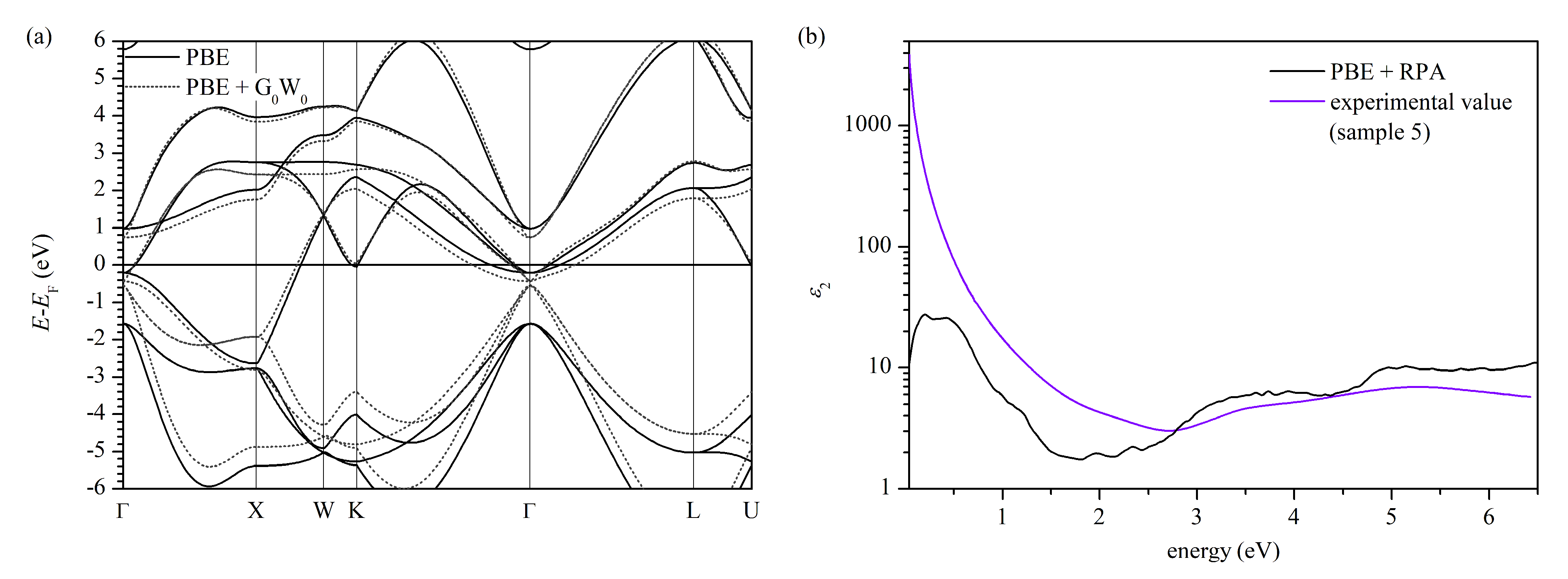
3.4. Ab Initio Calculations
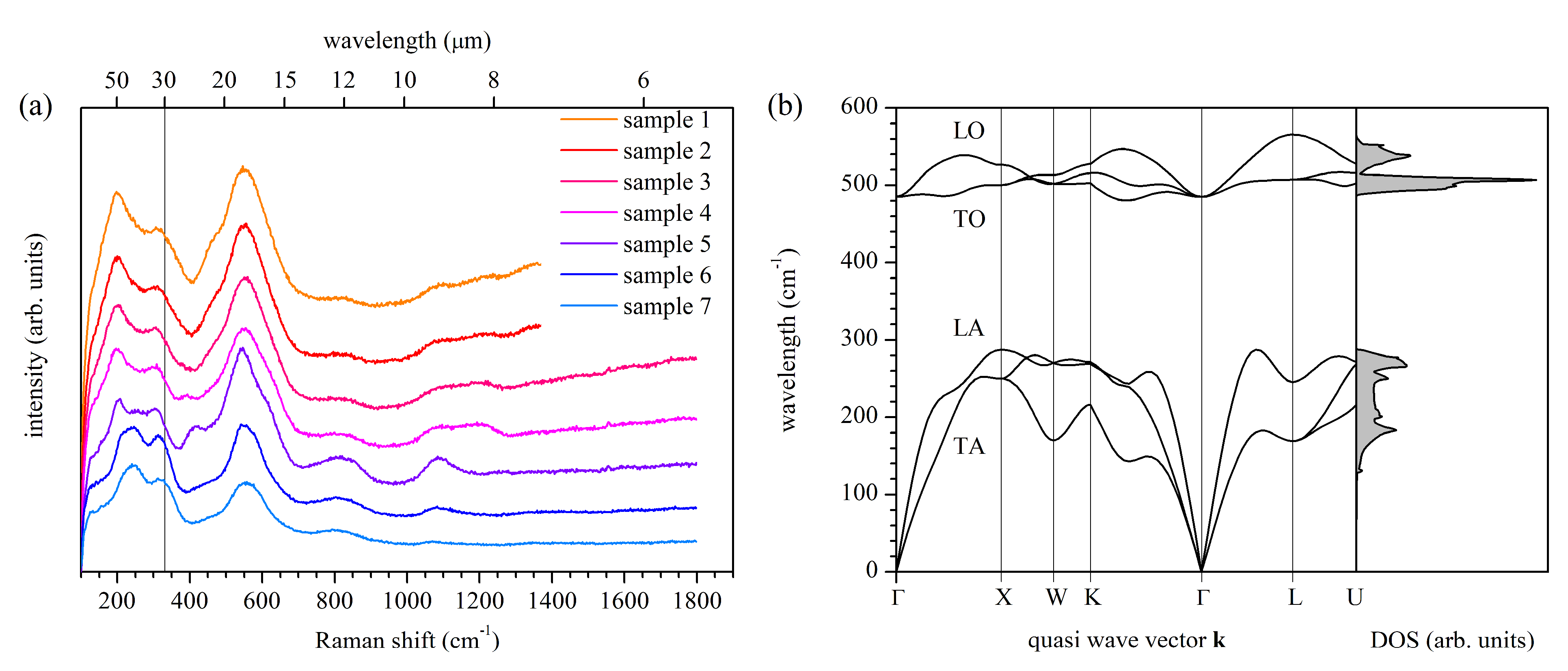
3.5. Raman Measurements
4. Conclusions
Supplementary Materials
Author Contributions
Funding
Institutional Review Board Statement
Informed Consent Statement
Data Availability Statement
Conflicts of Interest
Abbreviations
| AFM | Atomic Force Microscopy |
| CMOS | Complementary Metal-Oxide-Semiconductor |
| DFT | Density Functional Theory |
| EDS | Energy-dispersive X-ray spectroscopy |
| FTIR | Fourier transform infrared (spectroscopy) |
| GGA | Generalized Gradient Approximation |
| GIXRD | Grazing Incidence X-ray Diffraction |
| LO | Longitudinal Optical (phonon) |
| PBE | Perdew-Burke-Ernzerhof (parametrization) |
| RMS | Root-Mean-Square |
| RPA | Random-Phase Approximation |
| SEM | Scanning Electron Microscopy |
| SERS | Surface-Enhanced Raman Spectroscopy |
| SIMS | Secondary Ion Mass Spectroscopy |
| TO | Transverse Optical (phonon) |
| UV | Ultra-violet (spectral range) |
| VASE | Variable-Angle Spectroscopic Ellipsometry |
| VIS | Visible (spectral range) |
References
- Rebenne, H.E.; Bhat, D.G. Review of CVD TiN Coatings for Wear-Resistant Applications: Deposition Processes, Properties and Performance. Surf. Coat. Technol. 1994, 63, 1–13. [Google Scholar] [CrossRef]
- Nose, M.; Zhou, M.; Honbo, E.; Yokota, M.; Saji, S. Colorimetric Properties of ZrN and TiN Coatings Prepared by DC Reactive Sputtering. Surf. Coat. Technol. 2001, 142–144, 211–217. [Google Scholar] [CrossRef]
- Yokoyama, N.; Hinode, K.; Homma, Y. LPCVD Titanium Nitride for ULSIs. J. Electrochem. Soc. 1991, 138, 190–195. [Google Scholar] [CrossRef]
- Dauskardt, R.H.; Lane, M.; Ma, Q.; Krishna, N. Adhesion and Debonding of Multi-Layer Thin film Structures. Eng. Fract. Mech. 1998, 61, 141–162. [Google Scholar]
- Lemme, M.C.; Efavi, J.K.; Mollenhauer, T.; Schmidt, M.; Gottlob, H.D.B.; Wahlbrink, T.; Kurz, H. Nanoscale TiN Metal Gate Technology for CMOS Integration. Microelectron. Eng. 2006, 83, 1551–1554. [Google Scholar] [CrossRef]
- Naik, G.V.; Kim, J.; Boltasseva, A. Oxides and Nitrides as Alternative Plasmonic Materials in the Optical Range [Invited]. Opt. Mater. Express OME 2011, 1, 1090–1099. [Google Scholar] [CrossRef] [Green Version]
- Naik, G.V.; Schroeder, J.L.; Ni, X.; Kildishev, A.V.; Sands, T.D.; Boltasseva, A. Titanium Nitride as a Plasmonic Material for Visible and Near-Infrared Wavelengths. Opt. Mater. Express 2012, 2, 478. [Google Scholar] [CrossRef] [Green Version]
- Naik, G.V.; Shalaev, V.M.; Boltasseva, A. Alternative Plasmonic Materials: Beyond Gold and Silver. Adv. Mater. 2013, 25, 3264–3294. [Google Scholar]
- Naik, G.V.; Saha, B.; Liu, J.; Saber, S.M.; Stach, E.A.; Irudayaraj, J.M.K.; Sands, T.D.; Shalaev, V.M.; Boltasseva, A. Epitaxial Superlattices with Titanium Nitride as a Plasmonic Component for Optical Hyperbolic Metamaterials. Proc. Natl. Acad. Sci. USA 2014, 111, 7546–7551. [Google Scholar] [CrossRef] [Green Version]
- Huang, J.; Zhang, D.; Wang, H. Epitaxial TiN/MgO Multilayers with Ultrathin TiN and MgO Layers as Hyperbolic Metamaterials in Visible Region. Mater. Today Phys. 2021, 16, 100316. [Google Scholar] [CrossRef]
- Li, W.; Guler, U.; Kinsey, N.; Naik, G.V.; Boltasseva, A.; Guan, J.; Shalaev, V.M.; Kildishev, A.V. Refractory Plasmonics with Titanium Nitride: Broadband Metamaterial Absorber. Adv. Mater. 2014, 26, 7959–7965. [Google Scholar]
- Gui, L.; Bagheri, S.; Strohfeldt, N.; Hentschel, M.; Zgrabik, C.M.; Metzger, B.; Linnenbank, H.; Hu, E.L.; Giessen, H. Nonlinear Refractory Plasmonics with Titanium Nitride Nanoantennas. Nano Lett. 2016, 16, 5708–5713. [Google Scholar]
- Briggs, J.A.; Naik, G.V.; Petach, T.A.; Baum, B.K.; Goldhaber-Gordon, D.; Dionne, J.A. Fully CMOS-Compatible Titanium Nitride Nanoantennas. Appl. Phys. Lett. 2016, 108, 051110. [Google Scholar] [CrossRef]
- Kharintsev, S.S.; Kharitonov, A.V.; Saikin, S.K.; Alekseev, A.M.; Kazarian, S.G. Nonlinear Raman Effects Enhanced by Surface Plasmon Excitation in Planar Refractory Nanoantennas. Nano Lett. 2017, 17, 5533–5539. [Google Scholar] [CrossRef]
- Wen, X.; Li, G.; Gu, C.; Zhao, J.; Wang, S.; Jiang, C.; Palomba, S.; Martijn de Sterke, C.; Xiong, Q. Doubly Enhanced Second Harmonic Generation through Structural and Epsilon-near-Zero Resonances in TiN Nanostructures. ACS Photonics 2018, 5, 2087–2093. [Google Scholar] [CrossRef]
- Gadalla, M.N.; Greenspon, A.S.; Tamagnone, M.; Capasso, F.; Hu, E.L. Excitation of Strong Localized Surface Plasmon Resonances in Highly Metallic Titanium Nitride Nano-Antennas for Stable Performance at Elevated Temperatures. ACS Appl. Nano Mater. 2019, 2, 3444–3452. [Google Scholar] [CrossRef]
- Gadalla, M.N.; Chaudhary, K.; Zgrabik, C.M.; Capasso, F.; Hu, E.L. Imaging of Surface Plasmon Polaritons in Low-Loss Highly Metallic Titanium Nitride Thin Films in Visible and Infrared Regimes. Opt. Express 2020, 28, 14536. [Google Scholar] [CrossRef]
- Kaisar, N.; Huang, Y.-T.; Jou, S.; Kuo, H.-F.; Huang, B.-R.; Chen, C.-C.; Hsieh, Y.-F.; Chung, Y.-C. Surface-Enhanced Raman Scattering Substrates of Flat and Wrinkly Titanium Nitride Thin Films by Sputter Deposition. Surf. Coat. Technol. 2018, 337, 434–438. [Google Scholar] [CrossRef]
- Chaudhuri, K.; Guler, U.; Azzam, S.I.; Reddy, H.; Saha, S.; Marinero, E.E.; Kildishev, A.V.; Shalaev, V.M.; Boltasseva, A. Remote Sensing of High Temperatures with Refractory, Direct-Contact Optical Metacavity. ACS Photonics 2020, 7, 472–479. [Google Scholar] [CrossRef]
- Zgrabik, C.M.; Hu, E.L. Optimization of Sputtered Titanium Nitride as a Tunable Metal for Plasmonic Applications. Opt. Mater. Express 2015, 5, 2786. [Google Scholar] [CrossRef] [Green Version]
- Guo, W.-P.; Mishra, R.; Cheng, C.-W.; Wu, B.-H.; Chen, L.-J.; Lin, M.-T.; Gwo, S. Titanium Nitride Epitaxial Films as a Plasmonic Material Platform: Alternative to Gold. ACS Photonics 2019, 6, 1848–1854. [Google Scholar] [CrossRef]
- Chang, C.-C.; Nogan, J.; Yang, Z.-P.; Kort-Kamp, W.J.M.; Ross, W.; Luk, T.S.; Dalvit, D.A.R.; Azad, A.K.; Chen, H.-T. Highly Plasmonic Titanium Nitride by Room-Temperature Sputtering. Sci. Rep. 2019, 9, 15287. [Google Scholar] [CrossRef] [Green Version]
- Fomra, D.; Secondo, R.; Ding, K.; Avrutin, V.; Izyumskaya, N.; Özgür, Ü.; Kinsey, N. Plasmonic Titanium Nitride via Atomic Layer Deposition: A Low-Temperature Route. J. Appl. Phys. 2020, 127, 103101. [Google Scholar] [CrossRef]
- Chen, L.; Ran, Y.; Jiang, Z.; Li, Y.; Wang, Z. Structural, Compositional, and Plasmonic Characteristics of Ti–Zr Ternary Nitride Thin Films Tuned by the Nitrogen Flow Ratio in Magnetron Sputtering. Nanomaterials 2020, 10, 829. [Google Scholar] [CrossRef]
- Maurya, K.C.; Shalaev, V.M.; Boltasseva, A.; Saha, B. Reduced Optical Losses in Refractory Plasmonic Titanium Nitride Thin Films Deposited with Molecular Beam Epitaxy. Opt. Mater. Express 2020, 10, 2679. [Google Scholar] [CrossRef]
- Zhang, R.; Ma, Q.-Y.; Liu, H.; Sun, T.-Y.; Bi, J.; Song, Y.; Peng, S.; Liang, L.; Gao, J.; Cao, H.; et al. Crystal Orientation-Dependent Oxidation of Epitaxial TiN Films with Tunable Plasmonics. ACS Photonics 2021, 8, 847–856. [Google Scholar] [CrossRef]
- Shah, D.; Reddy, H.; Kinsey, N.; Shalaev, V.M.; Boltasseva, A. Optical Properties of Plasmonic Ultrathin TiN Films. Adv. Opt. Mater. 2017, 5, 1700065. [Google Scholar] [CrossRef]
- Shah, D.; Catellani, A.; Reddy, H.; Kinsey, N.; Shalaev, V.; Boltasseva, A.; Calzolari, A. Controlling the Plasmonic Properties of Ultrathin TiN Films at the Atomic Level. ACS Photonics 2018, 5, 2816–2824. [Google Scholar] [CrossRef] [Green Version]
- Patsalas, P.; Kalfagiannis, N.; Kassavetis, S. Optical Properties and Plasmonic Performance of Titanium Nitride. Materials 2015, 8, 3128–3154. [Google Scholar] [CrossRef] [Green Version]
- Patsalas, P.; Kalfagiannis, N.; Kassavetis, S.; Abadias, G.; Bellas, D.V.; Lekka, C.; Lidorikis, E. Conductive Nitrides: Growth Principles, Optical and Electronic Properties, and Their Perspectives in Photonics and Plasmonics. Mater. Sci. Eng. R Rep. 2018, 123, 1–55. [Google Scholar] [CrossRef]
- Edlou, S.M.; Simons, J.C.; Al-Jumaily, G.A.; Raouf, N.A. Optical and Electrical Properties of Reactively Sputtered TiN, ZrN, and HfN Thin Films. In Optical Thin Films IV: New Developments; International Society for Optics and Photonics: Bellingham, WA, USA, 1994; Volume 2262, pp. 96–106. [Google Scholar]
- Adachi, S.; Takahashi, M. Optical Properties of TiN Films Deposited by Direct Current Reactive Sputtering. J. Appl. Phys. 2000, 87, 1264–1269. [Google Scholar] [CrossRef]
- Patsalas, P.; Logothetidis, S. Optical, Electronic, and Transport Properties of Nanocrystalline Titanium Nitride Thin Films. J. Appl. Phys. 2001, 90, 4725–4734. [Google Scholar] [CrossRef]
- Karlsson, B.; Shimshock, R.P.; Seraphin, B.O.; Haygarth, J.C. Optical Properties of CVD-Coated TiN, ZrN and HfN. Sol. Energy Mater. 1983, 7, 401–411. [Google Scholar] [CrossRef]
- Cinali, M.B.; Coşkun, Ö.D. Improved Infrared Emissivity of Diamond-like Carbon Sandwich Structure with Titanium Nitride Metallic Interlayer. Sol. Energy 2020, 204, 644–653. [Google Scholar] [CrossRef]
- Ogawa, S.; Okada, K.; Fukushima, N.; Kimata, M. Wavelength Selective Uncooled Infrared Sensor by Plasmonics. Appl. Phys. Lett. 2012, 100, 021111. [Google Scholar] [CrossRef]
- De Luca, A.; Ali, S.Z.; Hopper, R.H.; Boual, S.; Gardner, J.W.; Udrea, F. Filterless non-dispersive infra-red gas detection: A proof of concept. In Proceedings of the 2017 IEEE 30th International Conference on Micro Electro Mechanical Systems (MEMS), Las Vegas, NV, USA, 22–26 January 2017; pp. 1220–1223. [Google Scholar]
- Xing, Y.; Urasinska-Wojcik, B.; Gardner, J.W. Plasmonic enhanced CMOS non-dispersive infrared gas sensor for acetone and ammonia detection. In Proceedings of the 2018 IEEE International Instrumentation and Measurement Technology Conference (I2MTC), Houston, TX, USA, 14–17 May 2018; pp. 1–5. [Google Scholar]
- Kresse, G.; Hafner, J. Ab Initio Molecular Dynamics for Liquid Metals. Phys. Rev. B 1993, 47, 558–561. [Google Scholar] [CrossRef]
- Kresse, G.; Hafner, J. Ab Initio Molecular-Dynamics Simulation of the Liquid-Metal–Amorphous-Semiconductor Transition in Germanium. Phys. Rev. B 1994, 49, 14251–14269. [Google Scholar] [CrossRef]
- Kresse, G.; Furthmüller, J. Efficiency of Ab-Initio Total Energy Calculations for Metals and Semiconductors Using a Plane-Wave Basis Set. Comput. Mater. Sci. 1996, 6, 15–50. [Google Scholar] [CrossRef]
- Kresse, G.; Furthmüller, J. Efficient Iterative Schemes for Ab Initio Total-Energy Calculations Using a Plane-Wave Basis Set. Phys. Rev. B 1996, 54, 11169–11186. [Google Scholar] [CrossRef]
- Blöchl, P.E. Projector Augmented-Wave Method. Phys. Rev. B 1994, 50, 17953–17979. [Google Scholar] [CrossRef] [Green Version]
- Kresse, G.; Joubert, D. From Ultrasoft Pseudopotentials to the Projector Augmented-Wave Method. Phys. Rev. B 1999, 59, 1758–1775. [Google Scholar] [CrossRef]
- Perdew, J.P.; Burke, K.; Ernzerhof, M. Generalized Gradient Approximation Made Simple. Phys. Rev. Lett. 1996, 77, 3865–3868. [Google Scholar] [CrossRef] [Green Version]
- Parlinski, K.; Li, Z.Q.; Kawazoe, Y. First-Principles Determination of the Soft Mode in Cubic ZrO2. Phys. Rev. Lett. 1997, 78, 4063–4066. [Google Scholar] [CrossRef]
- Togo, A.; Tanaka, I. First Principles Phonon Calculations in Materials Science. Scr. Mater. 2015, 108, 1–5. [Google Scholar] [CrossRef] [Green Version]
- Ehrenreich, H.; Cohen, M.H. Self-Consistent Field Approach to the Many-Electron Problem. Phys. Rev. 1959, 115, 786–790. [Google Scholar] [CrossRef]
- Gajdoš, M.; Hummer, K.; Kresse, G.; Furthmüller, J.; Bechstedt, F. Linear Optical Properties in the Projector-Augmented Wave Methodology. Phys. Rev. B 2006, 73, 045112. [Google Scholar] [CrossRef] [Green Version]
- Elstner, F.; Ehrlich, A.; Giegengack, H.; Kupfer, H.; Richter, F. Structure and Properties of Titanium Nitride Thin Films Deposited at Low Temperatures Using Direct Current Magnetron Sputtering. J. Vac. Sci. Technol. A Vac. Surf. Film. 1994, 12, 476–483. [Google Scholar] [CrossRef]
- Mahieu, S.; Ghekiere, P.; Depla, D.; De Gryse, R. Biaxial Alignment in Sputter Deposited Thin Films. Thin Solid Film. 2006, 515, 1229–1249. [Google Scholar] [CrossRef] [Green Version]
- Bendavid, A.; Martin, P.J.; Netterfield, R.P.; Kinder, T.J. Characterization of the Optical Properties and Composition of TiNx Thin Films by Spectroscopic Ellipsometry and X-Ray Photoelectron Spectroscopy. Surf. Interface Anal. 1996, 24, 627–633. [Google Scholar]
- Walker, C.G.H.; Matthew, J.A.D.; Anderson, C.A.; Brown, N.M.D. An Estimate of the Electron Effective Mass in Titanium Nitride Using UPS and EELS. Surf. Sci. 1998, 412–413, 405–414. [Google Scholar] [CrossRef]
- Srivastava, A.; Chauhan, M.; Singh, R.K. Pressure Induced Phase Transitions in Transition Metal Nitrides: Ab Initio Study: Pressure Induced Phase Transitions in Transition Metal Nitrides. Phys. Status Solidi B 2011, 248, 2793–2800. [Google Scholar] [CrossRef]
- Yu, S.; Zeng, Q.; Oganov, A.R.; Frapper, G.; Zhang, L. Phase Stability, Chemical Bonding and Mechanical Properties of Titanium Nitrides: A First-Principles Study. Phys. Chem. Chem. Phys. 2015, 17, 11763–11769. [Google Scholar] [CrossRef] [Green Version]
- Ding, K.; Fomra, D.; Kvit, A.V.; Morkoç, H.; Kinsey, N.; Özgür, Ü.; Avrutin, V. A Platform for Complementary Metal-Oxide-Semiconductor Compatible Plasmonics: High Plasmonic Quality Titanium Nitride Thin Films on Si (001) with a MgO Interlayer. Adv. Photonics Res. 2021, 2, 2000210. [Google Scholar] [CrossRef]
- Ern, V.; Switendick, A.C. Electronic Band Structure of TiC, TiN, and TiO. Phys. Rev. 1965, 137, A1927–A1936. [Google Scholar] [CrossRef]
- Ahuja, R.; Eriksson, O.; Wills, J.M.; Johansson, B. Structural, Elastic, and High-Pressure Properties of Cubic TiC, TiN, and TiO. Phys. Rev. B 1996, 53, 3072–3079. [Google Scholar] [CrossRef]
- Delin, A.; Eriksson, O.; Ahuja, R.; Johansson, B.; Brooks, M.S.S.; Gasche, T.; Auluck, S.; Wills, J.M. Optical Properties of the Group-IV B Refractory Metal Compounds. Phys. Rev. B 1996, 54, 1673–1681. [Google Scholar] [CrossRef]
- Marlo, M.; Milman, V. Density-Functional Study of Bulk and Surface Properties of Titanium Nitride Using Different Exchange-Correlation Functionals. Phys. Rev. B 2000, 62, 2899–2907. [Google Scholar] [CrossRef]
- Stampfl, C.; Mannstadt, W.; Asahi, R.; Freeman, A.J. Electronic Structure and Physical Properties of Early Transition Metal Mononitrides: Density-Functional Theory LDA, GGA, and Screened-Exchange LDA FLAPW Calculations. Phys. Rev. B 2001, 63, 155106. [Google Scholar] [CrossRef] [Green Version]
- Catellani, A.; Calzolari, A. Plasmonic Properties of Refractory Titanium Nitride. Phys. Rev. B 2017, 95, 115145. [Google Scholar] [CrossRef] [Green Version]
- Dal Forno, S.; Lischner, J. Electron-Phonon Coupling and Hot Electron Thermalization in Titanium Nitride. Phys. Rev. Mater. 2019, 3, 115203. [Google Scholar] [CrossRef] [Green Version]
- Höchst, H.; Bringans, R.D.; Steiner, P.; Wolf, T. Photoemission Study of the Electronic Structure of Stoichiometric and Substoichiometric TiN and ZrN. Phys. Rev. B 1982, 25, 7183–7191. [Google Scholar] [CrossRef]
- Anderson, C.A.; McKinley, A.; Brown, N.M.D.; Joyce, A.M. A Combined AES, Resonant Photoemission and EELS Study of in-Situ Grown Titanium Nitride. Surf. Sci. 1997, 383, 248–260. [Google Scholar]
- Harrison, W.A. Parallel-Band Effects in Interband Optical Absorption. Phys. Rev. 1966, 147, 467–469. [Google Scholar] [CrossRef]
- Ashcroft, N.W.; Sturm, K. Interband Absorption and the Optical Properties of Polyvalent Metals. Phys. Rev. B 1971, 3, 1898–1910. [Google Scholar] [CrossRef]
- Boyen, H.-G.; Gampp, R.; Oelhafen, P.; Heinz, B.; Ziemann, P.; Lauinger, C.; Herminghaus, S. Intraband Transitions in Simple Metals: Evidence for Non-Drude-like near-IR Optical Properties. Phys. Rev. B 1997, 56, 6502–6505. [Google Scholar] [CrossRef]
- Ehrenreich, H.; Philipp, H.R.; Segall, B. Optical Properties of Aluminum. Phys. Rev. 1963, 132, 1918–1928. [Google Scholar] [CrossRef]
- Nguyen, H.V.; An, I.; Collins, R.W. Evolution of the Optical Functions of Thin-Film Aluminum: A Real-Time Spectroscopic Ellipsometry Study. Phys. Rev. B 1993, 47, 3947–3965. [Google Scholar] [CrossRef]
- Chen, L.-Y.; Lynch, D.W. The Optical Properties of AuAl2 and PtAl2. Phys. Status Solidi 1988, 148, 387–394. [Google Scholar] [CrossRef]
- Kim, K.J.; Harmon, B.N.; Chen, L.-Y.; Lynch, D.W. Optical Properties and Electronic Structures of the Intermetallic Compounds AuGa2 and PtGa2. Phys. Rev. B 1990, 42, 8813–8819. [Google Scholar] [CrossRef] [Green Version]
- Spengler, W.; Kaiser, R.; Christensen, A.N.; Müller-Vogt, G. Raman Scattering, Superconductivity, and Phonon Density of States of Stoichiometric and Nonstoichiometric TiN. Phys. Rev. B 1978, 17, 1095–1101. [Google Scholar] [CrossRef]
- Constable, C.P.; Yarwood, J.; Münz, W.-D. Raman Microscopic Studies of PVD Hard Coatings. Surf. Coat. Technol. 1999, 116–119, 155–159. [Google Scholar] [CrossRef]
- Stoehr, M.; Shin, C.-S.; Petrov, I.; Greene, J.E. Raman Scattering from TiN x (0.67 ≤ x ≤ 1.00) Single Crystals Grown on MgO(001). J. Appl. Phys. 2011, 110, 083503. [Google Scholar] [CrossRef]
- Kharitonov, A.V.; Yanilkin, I.V.; Gumarov, A.I.; Vakhitov, I.R.; Yusupov, R.V.; Tagirov, L.R.; Kharintsev, S.S.; Salakhov, M.K. Synthesis and Characterization of Titanium Nitride Thin Films for Enhancement and Localization of Optical Fields. Thin Solid Film. 2018, 653, 200–203. [Google Scholar] [CrossRef]
- Cheng, P.; Ye, T.; Zeng, H.; Ding, J. Raman Spectra Investigation on the Pressure-Induced Phase Transition in Titanium Nitride (TiN). AIP Adv. 2020, 10, 045110. [Google Scholar] [CrossRef]
- Kress, W.; Roedhammer, P.; Bilz, H.; Teuchert, W.D.; Christensen, A.N. Phonon Anomalies in Transition-Metal Nitrides: TiN. Phys. Rev. B 1978, 17, 111–113. [Google Scholar] [CrossRef]
- Isaev, E.I.; Simak, S.I.; Abrikosov, I.A.; Ahuja, R.; Vekilov, Y.K.; Katsnelson, M.I.; Lichtenstein, A.I.; Johansson, B. Phonon Related Properties of Transition Metals, Their Carbides, and Nitrides: A First-Principles Study. J. Appl. Phys. 2007, 101, 123519. [Google Scholar] [CrossRef] [Green Version]
- Chen, S.; Kühne, P.; Stanishev, V.; Knight, S.; Brooke, R.; Petsagkourakis, I.; Crispin, X.; Schubert, M.; Darakchieva, V.; Jonsson, M.P. On the Anomalous Optical Conductivity Dispersion of Electrically Conducting Polymers: Ultra-Wide Spectral Range Ellipsometry Combined with a Drude–Lorentz Model. J. Mater. Chem. C 2019, 7, 4350–4362. [Google Scholar] [CrossRef] [Green Version]


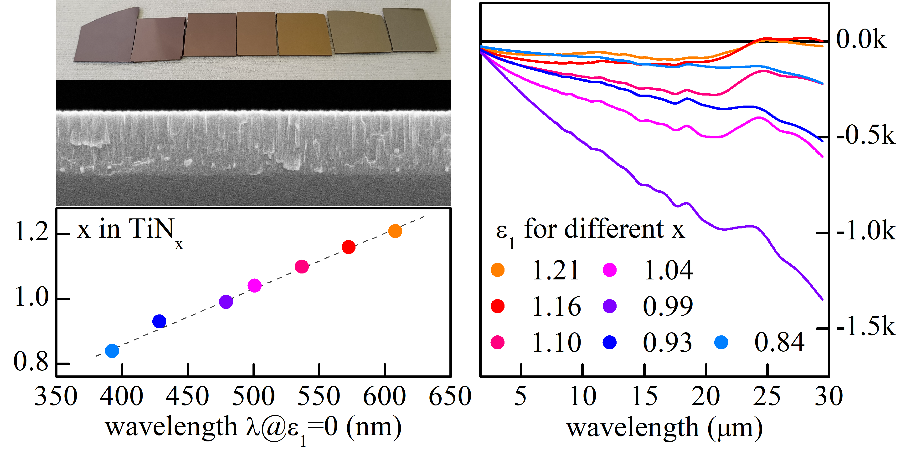
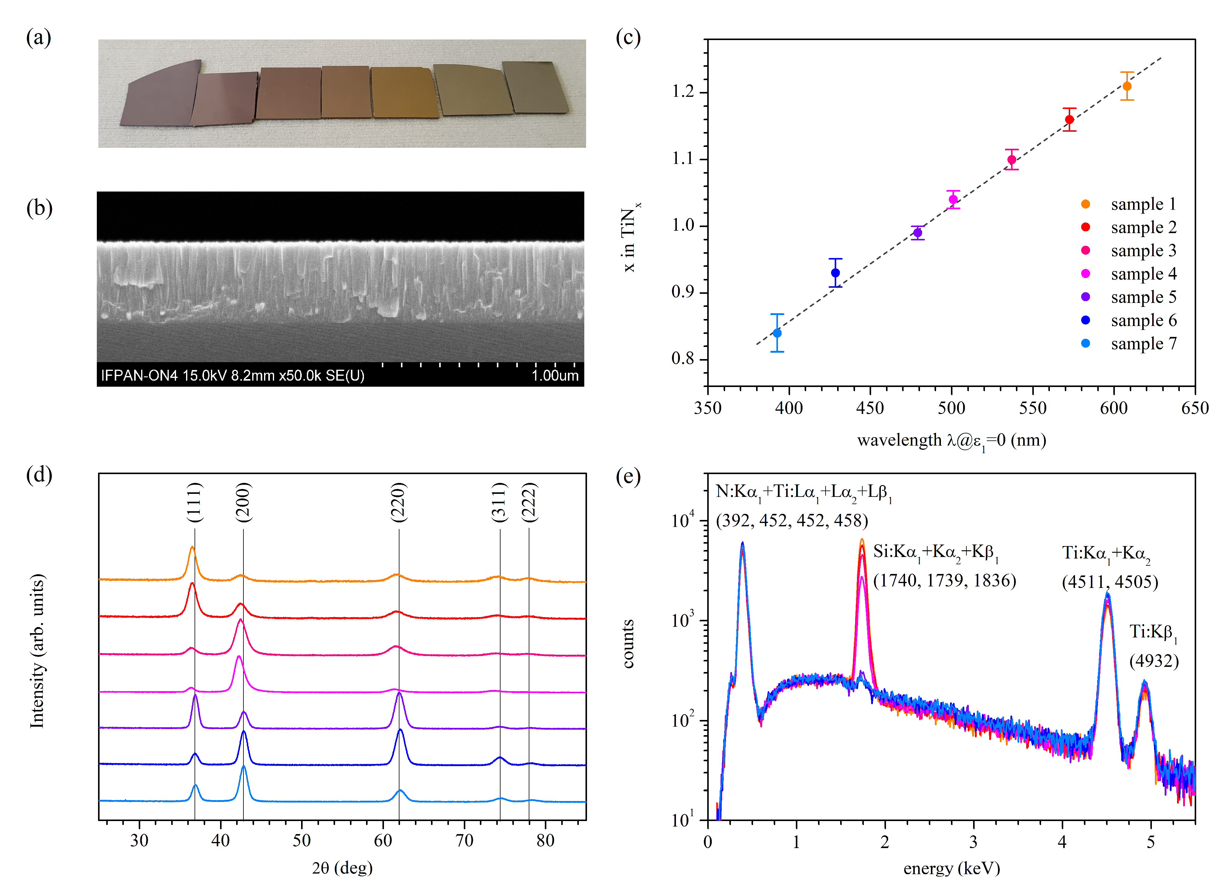
| # | d (nm) | RMS (nm) | λ@ε1 = 0 (nm) | x in TiNx − | a0 (nm) |
|---|---|---|---|---|---|
| 1 | 151 | 1.02 | 608.0 ± 0.5 | 1.21 ± 0.02 | 0.4260 |
| 2 | 169 | 0.99 | 572.5 ± 0.5 | 1.16 ± 0.02 | 0.4255 |
| 3 | 188 | 0.99 | 537.0 ± 0.5 | 1.10 ± 0.01 | 0.4263 |
| 4 | 230 | 0.96 | 501.0 ± 0.5 | 1.04 ± 0.01 | 0.4280 |
| 5 | 415 | 2.42 | 479.0 ± 0.5 | 0.99 ± 0.01 | 0.4234 |
| 6 | 515 | 2.43 | 428.5 ± 0.5 | 0.93 ± 0.02 | 0.4230 |
| 7 | 542 | 2.46 | 392.5 ± 0.5 | 0.84 ± 0.03 | 0.4220 |
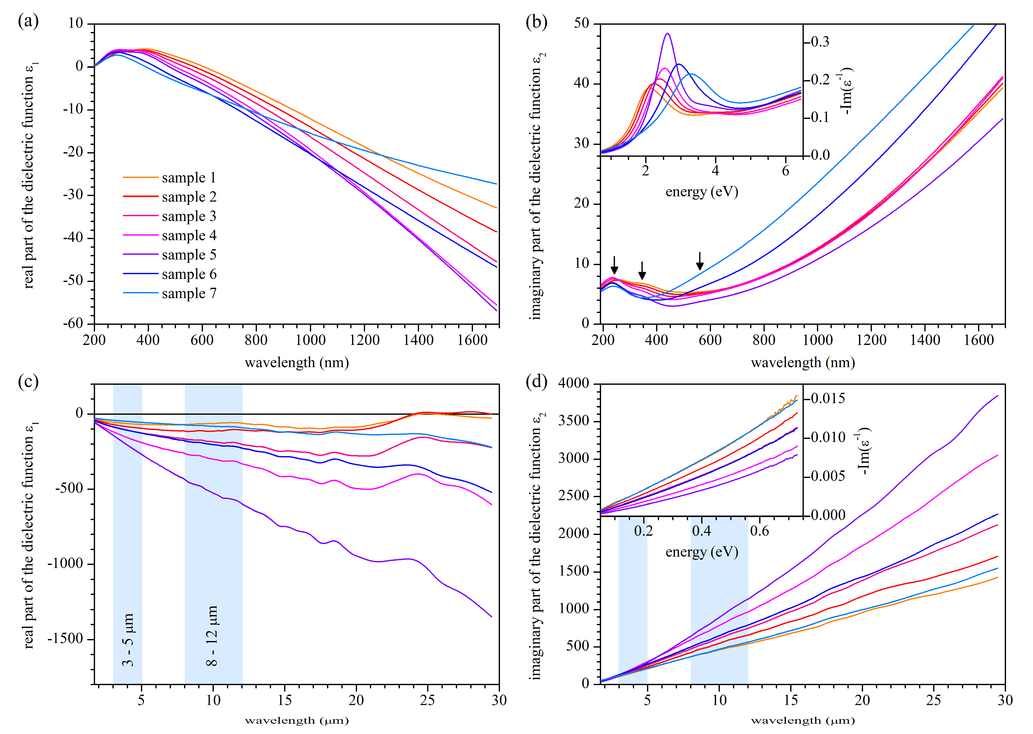
| Sample 1 | Sample 2 | Sample 3 | Sample 4 | Sample 5 | Sample 6 | Sample 7 | |
|---|---|---|---|---|---|---|---|
| (eV) | 6.61 | 6.73 | 6.80 | 6.82 | 6.30 | 7.42 | 8.22 |
| (eV) | 0.66 | 0.63 | 0.61 | 0.57 | 0.71 | 0.91 | 1.30 |
| f1 | 0.16 | 0.07 | 0.81 | 1.07 | 0.15 | 0.45 | 0.64 |
| (eV) | 2.39 | 2.30 | 2.30 | 2.15 | 2.16 | 2.17 | 2.22 |
| (eV) | 0.93 | 0.70 | 1.97 | 1.90 | 0.68 | 1.09 | 1.41 |
| f2 | 0.63 | 0.26 | 0.54 | 0.56 | 0.56 | 0.28 | - |
| (eV) | 3.49 | 3.51 | 3.60 | 3.67 | 3.68 | 3.85 | - |
| (eV) | 1.49 | 1.07 | 1.36 | 1.34 | 1.20 | 1.63 | - |
| f3 | 5.53 | 6.40 | 2.99 | 2.61 | 2.12 | 2.44 | 1.62 |
| (eV) | 5.54 | 5.84 | 5.19 | 5.20 | 5.16 | 5.34 | 5.07 |
| (eV) | 4.73 | 5.44 | 3.27 | 2.86 | 2.41 | 2.85 | 2.62 |
| f4 | 0.31 | 0.04 | 2.03 | 1.89 | 1.50 | 1.42 | 2.00 |
| (eV) | 6.68 | 6.47 | 6.76 | 6.56 | 6.43 | 6.76 | 6.63 |
| (eV) | 1.70 | 0.72 | 3.68 | 3.01 | 2.43 | 2.88 | 3.57 |
| Sample 1 | Sample 2 | Sample 3 | Sample 4 | Sample 5 | Sample 6 | Sample 7 | |
|---|---|---|---|---|---|---|---|
| (eV) | 6.45 | 6.40 | 6.57 | 6.70 | 6.10 | 7.13 | 8.10 |
| (eV) | 0.71 | 0.57 | 0.58 | 0.47 | 0.35 | 0.68 | 1.19 |
| (eV) | - | - | 1.32 | 2.41 | 4.97 | 2.07 | 0.93 |
| (eV) | - | - | 0.065 | 0.065 | 0.061 | 0.070 | 0.075 |
Publisher’s Note: MDPI stays neutral with regard to jurisdictional claims in published maps and institutional affiliations. |
© 2021 by the authors. Licensee MDPI, Basel, Switzerland. This article is an open access article distributed under the terms and conditions of the Creative Commons Attribution (CC BY) license (https://creativecommons.org/licenses/by/4.0/).
Share and Cite
Judek, J.; Wróbel, P.; Michałowski, P.P.; Ożga, M.; Witkowski, B.; Seweryn, A.; Struzik, M.; Jastrzębski, C.; Zberecki, K. Titanium Nitride as a Plasmonic Material from Near-Ultraviolet to Very-Long-Wavelength Infrared Range. Materials 2021, 14, 7095. https://0-doi-org.brum.beds.ac.uk/10.3390/ma14227095
Judek J, Wróbel P, Michałowski PP, Ożga M, Witkowski B, Seweryn A, Struzik M, Jastrzębski C, Zberecki K. Titanium Nitride as a Plasmonic Material from Near-Ultraviolet to Very-Long-Wavelength Infrared Range. Materials. 2021; 14(22):7095. https://0-doi-org.brum.beds.ac.uk/10.3390/ma14227095
Chicago/Turabian StyleJudek, Jarosław, Piotr Wróbel, Paweł Piotr Michałowski, Monika Ożga, Bartłomiej Witkowski, Aleksandra Seweryn, Michał Struzik, Cezariusz Jastrzębski, and Krzysztof Zberecki. 2021. "Titanium Nitride as a Plasmonic Material from Near-Ultraviolet to Very-Long-Wavelength Infrared Range" Materials 14, no. 22: 7095. https://0-doi-org.brum.beds.ac.uk/10.3390/ma14227095