
A Review on Chemical Vapour Deposition of Two-Dimensional MoS2 Flakes


IMEM-CNR, Parco Area delle Scienze 37A, 43124 Parma, Italy
*
Authors to whom correspondence should be addressed.
Materials 2021, 14(24), 7590; https://0-doi-org.brum.beds.ac.uk/10.3390/ma14247590
Submission received: 28 October 2021
/
Revised: 2 December 2021
/
Accepted: 7 December 2021
/
Published: 10 December 2021
(This article belongs to the Special Issue Feature Papers in Electronic Materials Section)
Abstract
:Two-dimensional (2D) materials such as graphene, transition metal dichalcogenides, and boron nitride have recently emerged as promising candidates for novel applications in sensing and for new electronic and photonic devices. Their exceptional mechanical, electronic, optical, and transport properties show peculiar differences from those of their bulk counterparts and may allow for future radical innovation breakthroughs in different applications. Control and reproducibility of synthesis are two essential, key factors required to drive the development of 2D materials, because their industrial application is directly linked to the development of a high-throughput and reliable technique to obtain 2D layers of different materials on large area substrates. Among various methods, chemical vapour deposition is considered an excellent candidate for this goal thanks to its simplicity, widespread use, and compatibility with other processes used to deposit other semiconductors. In this review, we explore the chemical vapour deposition of MoS2, considered one of the most promising and successful transition metal dichalcogenides. We summarize the basics of the synthesis procedure, discussing in depth: (i) the different substrates used for its deposition, (ii) precursors (solid, liquid, gaseous) available, and (iii) different types of promoters that favour the growth of two-dimensional layers. We also present a comprehensive analysis of the status of the research on the growth mechanisms of the flakes.
1. Introduction
The information technology revolution is driven by the continuous improvement of electronic devices and their constant scaling down. However, this process is rapidly approaching its limit. In order to continue the innovation process, introduction of new concepts and new materials is required. Some solutions have been identified in (i) the use of strain engineering and high-k gate dielectrics, (ii) silicon–germanium (SiGe) alloys and germanium, because of their higher electron mobility and lower need for power, and (iii) nanostructures and 2D materials, for the possibility of introducing brand-new device designs and concepts.
For the latter, graphene and similar 2D materials recently emerged as promising candidates because they exhibit interesting mechanical, electronic, optical, and transport properties with peculiar differences from those of their bulk counterparts. Graphene, despite its exceptional physical properties, has the major drawback of lacking an electronic bandgap, a limit that poses problems in realizing logic circuits and transistors. Bandgap engineering in graphene, although possible, has several drawbacks, such as increased complexity of the process and degradation of material quality, so it is not usually considered a viable choice for certain applications.
Transition metal dichalcogenides (TMD), silicon, germanium, and boron nitride can be thinned down to monolayers similarly to graphene, exhibiting weak interplane interaction and strong in-plane bonds. MoS2 is one of the most promising materials of this family because of the relative easiness of its synthesis and its interesting physical properties. It exhibits a hexagonal lattice structure consisting of a layer of transition metal atoms embedded in two chalcogen layers, with strong covalent bonds in each 2D plane and a weaker interaction between different planes. The properties of MoS2, similarly to those of other 2D materials, depend mainly on the vertical thickness of MoS2 rather than its lateral size. The most important difference with respect to graphene is that 2D MoS2 shows a direct bandgap of about 1.8 eV, making it an ideal candidate for applications in electronics, photonics, photovoltaics, energy storage, and catalysis [1].
Several proof-of-concept MoS2 devices have been already demonstrated. FETs with mobility up to 320 cm2 V−1 s−1 and on/off ratio of 108 at room temperature were realized [2,3], as well as inverters with gain up to 16 [4]. Several kinds of phototransistors, photosensors [5], and gas and biological sensors [6] were demonstrated, and the mechanical properties of MoS2 were exploited in the realization of strain sensors [7]. Moreover, the light emission properties of this material are also attracting considerable interest [8,9,10,11].
The future development of research is trending towards the integration of different building blocks and different 2D materials into a single device, aiming for the fabrication of high-performance CMOS-based circuits, sensors, and efficient photocatalytic systems [12,13].
The interest in developing new devices from 2D structures is also driven by several novel properties observed in these materials, such as valley polarization, in which conduction and valence bands of MoS2 monolayers present two inequivalent valleys at points K and K0, giving a new degree of freedom to carriers. This would permit radical new device concepts based on valleytronics and on spin–valley coupling, permitting control of information using circular polarized light [14].
Despite the results obtained so far on MoS2 devices and transistors in particular, it was observed that their performance was still far from the best theoretical predictions. The transport properties of MoS2 are limited by defects such as vacancies, antisites, charge traps, grain boundaries, and Coulomb impurities at the flake interface [15,16]. For example, the maximum predicted electron mobility of MoS2 at room temperature is about 410 cm2 V−1 s−1, leaving room for improvement. Understanding these limits and how to overcome them is a major issue on the MoS2 roadmap.
Reliable and controlled doping in MoS2 flakes is also a fundamental requirement to achieve precise control of their electrical and optical properties. Usually, substitutional doping is the dominating process as compared to interstitial doping. On this topic, fundamental contributions were the very recent reviews of Lin et al. [17] and Rai et al. [18], who considered the issues of Schottky barriers and contact resistance at the interface between MoS2 and a metal and the problems related to the doping of a wide range of 2D TMD materials, respectively. N-type doping of MoS2 could be obtained by adding ReO3 to the solid precursors [19] or by using ZnS as a sulfur precursor [20], while chloride permitted decreasing the resistivity of MoS2 flakes from some KΩ to about 0.5 KΩ, allowing for the realization of Schottky barriers with enhanced properties [21]. p-doping could be obtained by adding Nb2O5 to NaCl promoter when using solid precursors [22].
Another topic of particular interest is the possibility of including elements such as manganese (Mn) and iron (Fe), aiming to add new functionalities related to magnetism and spin to MoS2. First reports indicated the possibility of incorporating Mn in MoS2, but with some issues relative to the substrate used, as Mn was detected only in structures deposited on graphene and not on those deposited on SiO2/Si [23].
Despite their peculiar properties and the achievements so far obtained, the controllable synthesis of large-area flakes and the reproducibility of the process are still challenging issues; these are two essential, key factors required to sustain the future development of 2D materials. Mechanical exfoliation has so far granted a very high material quality, leading to the realization of devices and to an in-depth study of their properties. However, this method is very impractical and poses many limits on large-scale production. Industrial application of TMD is directly linked to the development of a high-throughput and reliable technique to obtain 2D layers of different materials on large area substrates, with a simple, reproducible, and scalable method. Chemical vapour deposition (CVD) is a good candidate for this task, since it has already been widely adopted for the mass production of many kinds of devices based on III-V and III-N materials and has thus the potential to permit the integration of 2D materials with “standard” semiconductors or other compounds. Many excellent reviews on MoS2 are already available, giving a broad scenario of all the work done on this material [24,25].
Although MoS2 flakes with large size (>500 μm) have been obtained with relevant success from several groups [26,27,28], in our opinion, research is still needed on many points that are usually overlooked: (i) the effect of different parameters (such as carriers’ flows or sulfur partial pressure), (ii) the possibility of engineering layers by surface treatments—this is crucial for the realization of heterostructures and possibly hybrid nanostructures, (iii) the growth reproducibility of these structures. It is a common experience to not be able to obtain the same 2D layers in different growth runs, and this is still a consistent problem for the technology’s transfer towards industrial applications. A reliable growth protocol that can be transferred to different reactors with minimal setup time is a strong requirement to allow 2D MoS2 to make the jump to mass production.
The preparation of this material is still challenging, and there is a lot of room for improving both the process and the material quality. Despite its relative simplicity, CVD remains one of the most widely used techniques to synthesize TMD flakes. Recently, new protocols and precursors have been introduced to optimize the deposition, to obtain better quality material, and to improve the reproducibility of the process.
The aim of this work was to collect and critically present the knowledge acquired so far in this field, providing the reader with a comprehensive review of the state of the art of the CVD growth processes used to prepare MoS2.
2. CVD Setup for Growth of MoS2
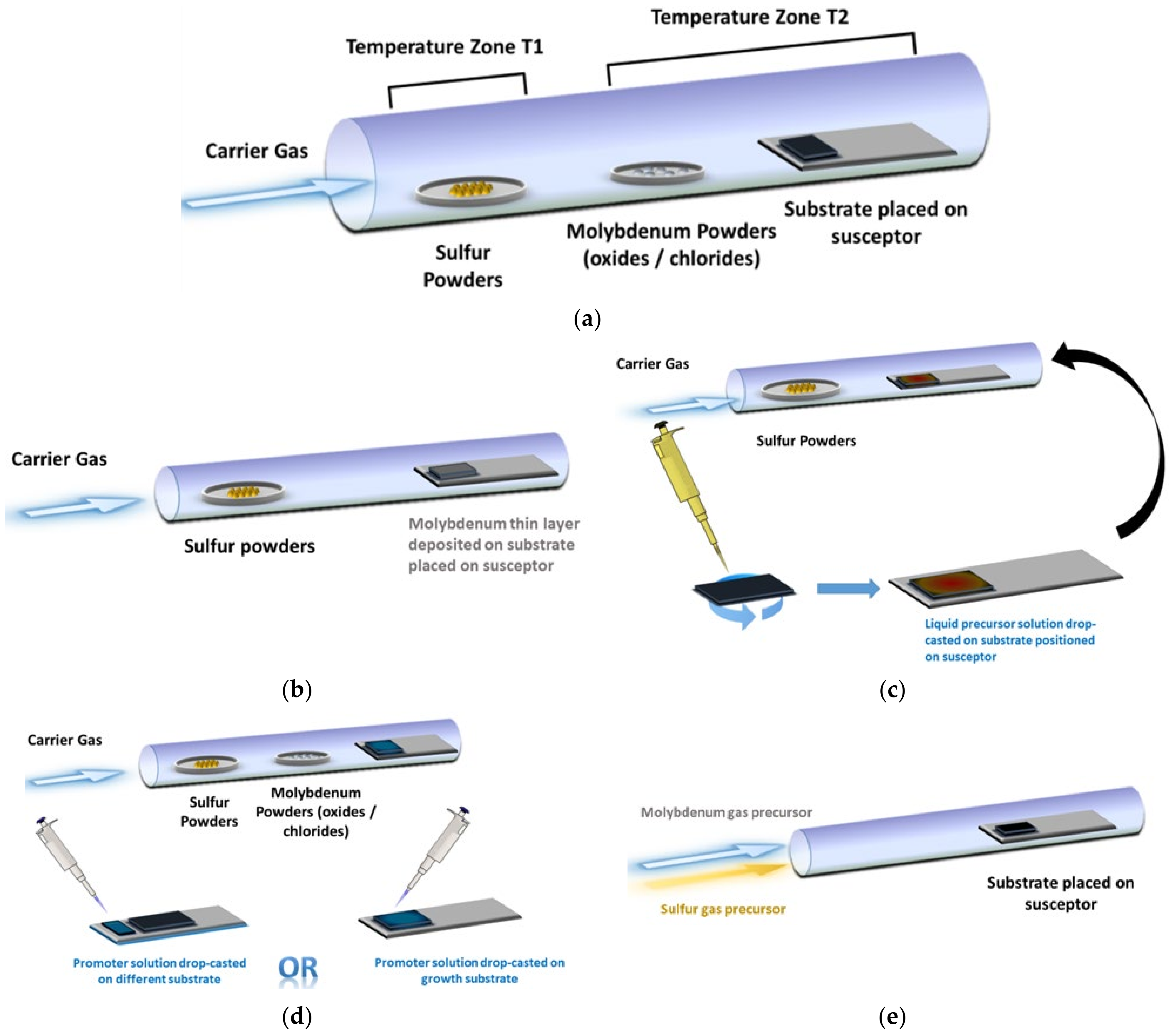
The basic concept of CVD is very simple, and it is schematically presented in Figure 1a: the precursors—either only S or both S and Mo compounds—are delivered in gaseous form to a substrate (placed on a susceptor of graphite or similar material) kept at high temperature, where the chemical reactions needed for the deposition of MoS2 occur. Most of the results reported in literature have been obtained using a standard horizontal reactor, such as that sketched in Figure 1. This configuration, although widely used, has the drawback of a nonuniform precursor gradient along the flow direction, resulting in a nonuniform deposition and in intrinsic difficulty in optimizing the growth parameter, since small changes in substrate position or in precursor supply may cause nonreproducible results. Development of vertical CVD reactors may help in solving these issues, since with this configuration, temperature and precursor supply may be more easily controlled and homogenized [29].
In the standard horizontal configuration, a quartz tube about 1 m long with a diameter of 2–5 cm is used. The heating is provided by a resistance placed around the tube. The reaction for MoS2 deposition requires a temperature in the 600–800 °C range, but in some cases, the supply of sulfur requires a second heating zone in the 100–200 °C range. In this case, to obtain better reproducibility and control, it is more convenient to separately and independently heat this additional zone (T2 in Figure 1a) in which the sulfur precursor is placed.
It is also possible to deposit the molybdenum precursors directly on the substrate, either in solid form (Figure 1b) or as a liquid solution (Figure 1c). Growth promoters, to obtain better control of the process, can be added either directly on the growth substrate or on a different substrate (Figure 1d). As a last method, the use of gaseous precursors (Figure 1e) avoids the need for placing the precursors inside the tube before the beginning of the process.
A standard routine to minimize the contamination from external air and O2 in the reaction tube is to purge the system with inert gas several times before starting the growth, eventually evacuating the tube with a rotary pump and then flushing with purified Ar or N2 up to ambient pressure, repeating this procedure several times.
The actual CVD process depends on the chemical status of the used precursors (solid, liquid, gaseous), but it is nevertheless possible to divide it into the following steps:
The precursors are brought into gaseous form and diluted in an inert carrier gas; e.g., powders are evaporated/sublimated, or a controlled amount of gas is measured by means of a mass flow controller.
The reactive species are transported by the carrier gas to the substrate. Chemical reactions may also occur in this step, e.g., reducing reactions.
The precursors diffuse towards the substrate surface.
The precursors are adsorbed at the surface, where adatom adsorption and migration occurs. The MoS2 flakes synthesis occurs in this step. By-products re-evaporate or desorb into the gas streams and are carried away into the exhaust.
The heating ramp times are usually in the range of 10–30 min from room temperature to growth temperature. The heating of sulfur powders typically starts when the substrate is already at the target temperature; this permits avoiding injecting S into the system before a constant substrate temperature is reached, limiting prereactions. The MoS2 growth proceeds for about 10–20 min, and then the system naturally cool downs to ambient temperature. If powders are used as reagents, heating of the substrate and of the MoO3 powders occurs simultaneously, since they are usually placed very near the substrate. This means that Mo starts to evaporate before the substrate reaches the target temperature.
Flake synthesis is dependent on different parameters such as the growth temperature and the distance between the substrate and the powders. Flow rate, chamber pressure, precursor supply, powder dimension, and purity also affect the final outcome of the growth. Despite the simplicity of the process, if excellent control is not achieved, the results may not be completely reproducible, and large-scale deposition can be very hard to obtain.
While it has been shown that different carrier gases can strongly influence the growth of graphene [30], considerably less attention has been devoted to this topic for the growth of MoS2. Considering that S is a strong reducing agent, the use of a purified inert gas (N2 or Ar) is usually sufficient for the sulfurization reaction to occur, and the carrier gases can be considered as inert in the reactions at the basis of 2D nucleation and growth. The use of H2 is thus not common in the MoS2 CVD process. Nevertheless, it was argued that H2 can have beneficial effects, as it can inhibit the thermally induced etching effect and promote the desulfurization reaction [31]. By carefully adjusting the amount of hydrogen in a H–Ar mixed carrier gas, authors were able to obtain layers with high crystallinity and a nearly perfect S/Mo atomic ratio. It was also suggested that, in the case of MoS2 growth using Mo(CO)6 with (C2H5)2S as precursors, the presence of H2 is necessary for removing carbonaceous species generated during the MOCVD growth, permitting increasing the average grain size from hundreds of nanometres to more than 10 μm [32].
Carrier gas flow rate was reported to affect the morphology of flakes, as well as their size and density: lowering the gas carrier flow during the heating stage from 35 to 15 sccm permitted increasing the density and size of the flakes [33]. Moreover, the shape of MoS2 flakes changed from zigzag to triangular as the gas carrier flow was decreased, indicating higher material quality. This behaviour was directly related to the quantity of S in the gas phase. As the carrier flow increased, the S transport grew more efficient, and S reacted with MoO3 powders, suppressing their evaporation, lowering MoO3 partial pressure, and promoting zigzag edge termination.
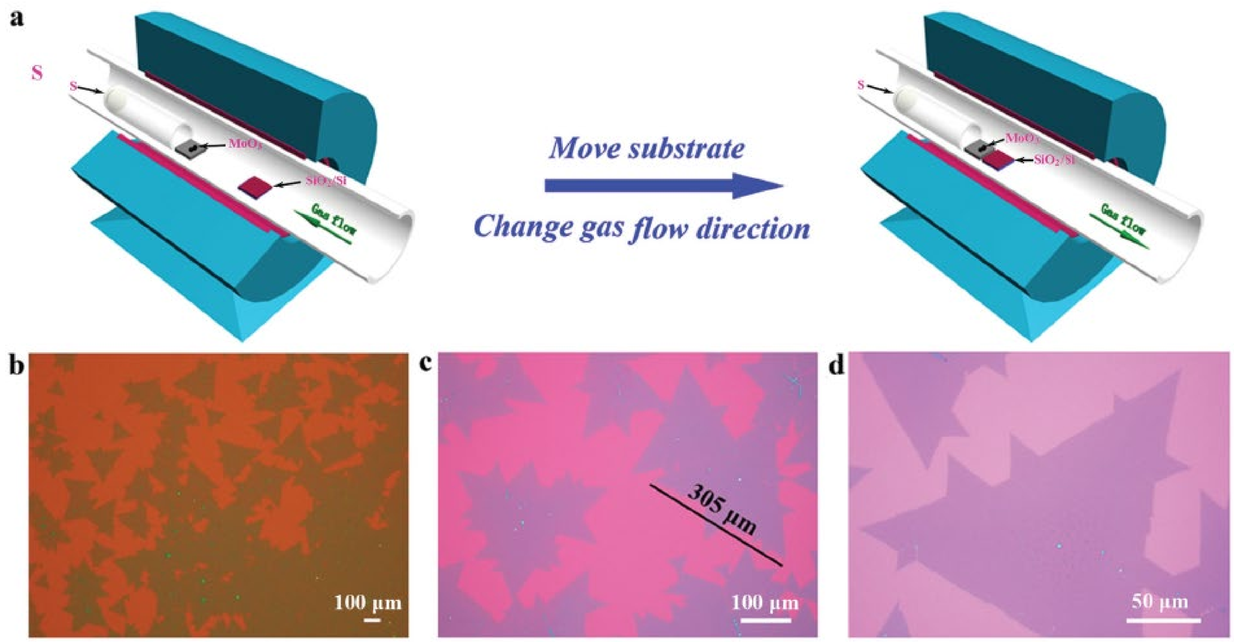
In order to have better control over S and MoO3 reactions during the heating stage of the process, a procedure of “flow reversal” was proposed [34]. During the heating of the furnace, Ar was introduced from the side of the Mo powders towards the side of the S powders (Figure 2). In this way, S reached neither the substrate nor the Mo powders, and any unintentional reaction was prevented; growth and nucleation of MoS2 far from the steady growth regime was inhibited. Once the setpoint temperatures of both substrate and S powders were reached, the Ar flow direction was switched back to the standard direction, so that it entered from the S powder side and delivered S vapours to the Mo powders and the substrate. Using this two-stage growth, the mean side length of MoS2 flakes was increased up to 250–300 μm.
Another custom setup to obtain better control of the precursor supply and to avoid cross-contamination of MoO3 and S powders consisted of placing S powders in a small tube nested inside another, larger tube so that S did not contaminate the MoO3 powders before entering the reaction zone [35].
3. Substrates
A typical characteristic of 2D materials is the very weak interlayer Van der Waals forces, in contrast with the stronger in-layer chemical bonds, which are ionic or covalent. This is the reason why bulk crystals of TMD materials, and MoS2 in particular, can be easily cleaved and exfoliated to produce few-layer flakes. As a consequence, the dangling bonds of the 2D plane are relatively inactive, and few interactions occur out-of-plane. For this reason, one could argue that in the 2D synthesis, the substrate’s role should be less important with respect to standard epitaxy, in which lattice and thermal matching conditions between the substrate and the epilayer are of paramount importance, determining whether defects are generated at the interface. The weak interactions between the substrate and the 2D layer reduce the importance of lattice mismatch, but the choice of the substrate remains an important parameter, not to be overlooked. The reason should be sought in the processes still occurring at the substrate surface that involve the reactive species, such as adsorption, diffusion, and nucleation. It was indeed observed that the substrate played an important role in influencing both the growth process and the properties of 2D layers, as evidenced in the excellent review on this topic in [36].
SiO2/Si substrate is the most commonly used for CVD synthesis of MoS2 because of: (i) the ease of observing and characterizing flakes on it through optical microscopy (from this point of view, the thickness of the oxide layer is of paramount importance [37]); (ii) its high melting point; (iii) its compatibility with silicon processing. On the other hand, for further characterization and/or applications, it is necessary to transfer the 2D material from the SiO2/Si substrate on other substrates or TEM grids. This implies a delicate chemical process composed of various steps: (i) coating of the material with poly(methyl methacrylate) (PMMA) film on the MoS2 layers by spin coating, (ii) etching of the SiO2 layer to separate it from the Si substrate in a solution (KOH, HF, NaOH), (iii) transfer of the floating PMMA/MoS2 film from the surface of the solution to the substrate of interest, and (iv) removal of the PMMA coating by rinsing in acetone and isopropanol [38].
The possibility of growing MoS2 on rigid metals has been investigated, in particular for the case of gold, as it was demonstrated that excellent nanostructures can be obtained on Au foils [39]. If one considers surfaces of Au(111), very large nanoflakes can be obtained [40] thanks to the lattice matching between Au(111) and MoS2 and the fact that the step edge of Au(111) favours the unidirectional nucleation of the film. The advantage of this substrate was confirmed recently in [41], where a unidirectional growth ratio over 99% of MoS2 flakes was achieved on Au(111) films sputtered on c-sapphire. The growth on Ag(111) was also demonstrated, opening up interesting perspectives on the realization of metal contacts on this 2D material [42].
Liquid metals are interesting, as their uniform and smooth surface can inhibit the inhomogeneous nucleation of 2D materials. Although convincing results have been published on other 2D materials, the growth of MoS2 on these substrates has been reported only for the MoS2/h-BN heterojunction grown on liquid metal Ni–Ga alloy [43].
MoS2 has also been grown with considerable success on c-sapphire, as it has a stable hexagon single crystal structure, matching the lattice symmetry of 2D material [27,44,45]. Sapphire surface can be prepared with a thermal treatment at 1100 °C before MoS2 growth to obtain a clean and atomically flat surface. Scaling up to a Metal–Organic Vapour Phase Epitaxy (MOVPE) process for 6-inch wafers was obtained, and the possibility of transferring the obtained flakes to a secondary carrier substrate opens up the possibility to reuse the sapphire substrate, making this choice an interesting alternative to the common SiO2/Si approach [46]. Very recently, the growth of monolayer flakes as large as 50 μm on a C-plane sapphire was demonstrated by designing the miscut orientation towards the A axis. This resulted in a break in the degeneracy of nucleation energy for the antiparallel MoS2 domains [47].
The growth of a 6-inch uniform monolayer of MoS2 on solid soda-lime glass was achieved because of the advantageous effect of sodium in enhancing the formation of flakes that were homogenously distributed in glass [48]. Na acts as a growth promoter; its effects are discussed in depth in a subsequent section
Recently, the possibility of growing MoS2 on flexible substrates such as polyimide was reported [49]. The issues related to the stability of the substrate were solved thanks to a CVD growth protocol allowing for low temperatures (<300 °C), and the feasibility of developing flexible gas sensors taking advantage of the properties of MoS2 was demonstrated.
In an interesting work, MoS2 monolayers were reproducibly deposited on a variety of substrates, amorphous (SiO2/Si and fused quartz), crystalline (bare Si and sapphire), and layered-flexible (mica), using the same growth conditions with solid precursors and mixed NaCl [50].
CVD growth of MoS2 on gallium nitride (GaN) was also reported, a very relevant step towards the realization of heterostructures for many applications [51]. This possibility is of particular interest because it would eliminate the delicate step of detachment and transfer of 2D flakes, allowing realizing MoS2 heterojunctions directly on a nitride template.
Following the ideas widely explored with III-N and III-V semiconductors, in which AlGaAs–InGaAs or AlGaN–InGaN heterostructures are used to exploit the possibility of bandgap engineering to design advanced devices, an emerging topic of research is the realization of so-called 2D Van der Waals heterostructures. By vertically stacking layers of different 2D materials coupled by very weak forces, it would be possible to avoid the presence of defects due to lattice mismatch observed in conventional 3D heterostructures [52]. A considerable effort has thus been devoted to exploring the synthesis of MoS2 and other 2D compounds onto graphene and other 2D materials. First results highlighted how it was possible to obtain high-quality 2D flakes by adding some gases to gas carriers (N or Ar) for the treatment of graphene surfaces, such as H2 [53] or ozone [54]. This allows for the preparation of high-quality nanoflakes of MoS2 because of the reduction in the oxidation of graphene during the growth process.
In [55,56], few-layer MoS2 was grown on graphene oxide films or flakes. These results suggested that carbon-based materials can significantly promote the growth rate and yield of MoS2. In [57], the differences in using graphene, sapphire, and SiO2/Si substrates were investigated, highlighting the role of surface diffusion mechanisms in determining different properties of MoS2 flakes. The authors remarked that the growth on graphene was very stable, resulting in the realization of a strain-free 2D layer.
A topic of paramount importance for the development of nanodevices is the growth on patterned substrates to increase the spatial control of MoS2 nanoflakes and to obtain a controlled nucleation only on certain substrate zones. The first pioneering work on this issue was the one by Najmaei et al. [58], who observed a catalytic effect of the edges of the substrate. Based on this effect, authors proposed and demonstrated a method to control the growth of 2D flakes using lithography to pattern the substrate. Later, it was demonstrated that, by using patterned seeds of molybdenum, it was possible to obtain flakes of MoS2 at predetermined locations with a good spatial resolution [59]. Another approach to control the nucleation site of MoS2 flakes was to use droplets of (NH4)2MoS4 in dimethyl-formamide suspended from the tip of a micropipette that is dragged across a sapphire single-crystalline substrate by a controlled substrate movement. This resulted in MoS2 films with alternating mono- and few-layer regions that had distinct optical properties [60].
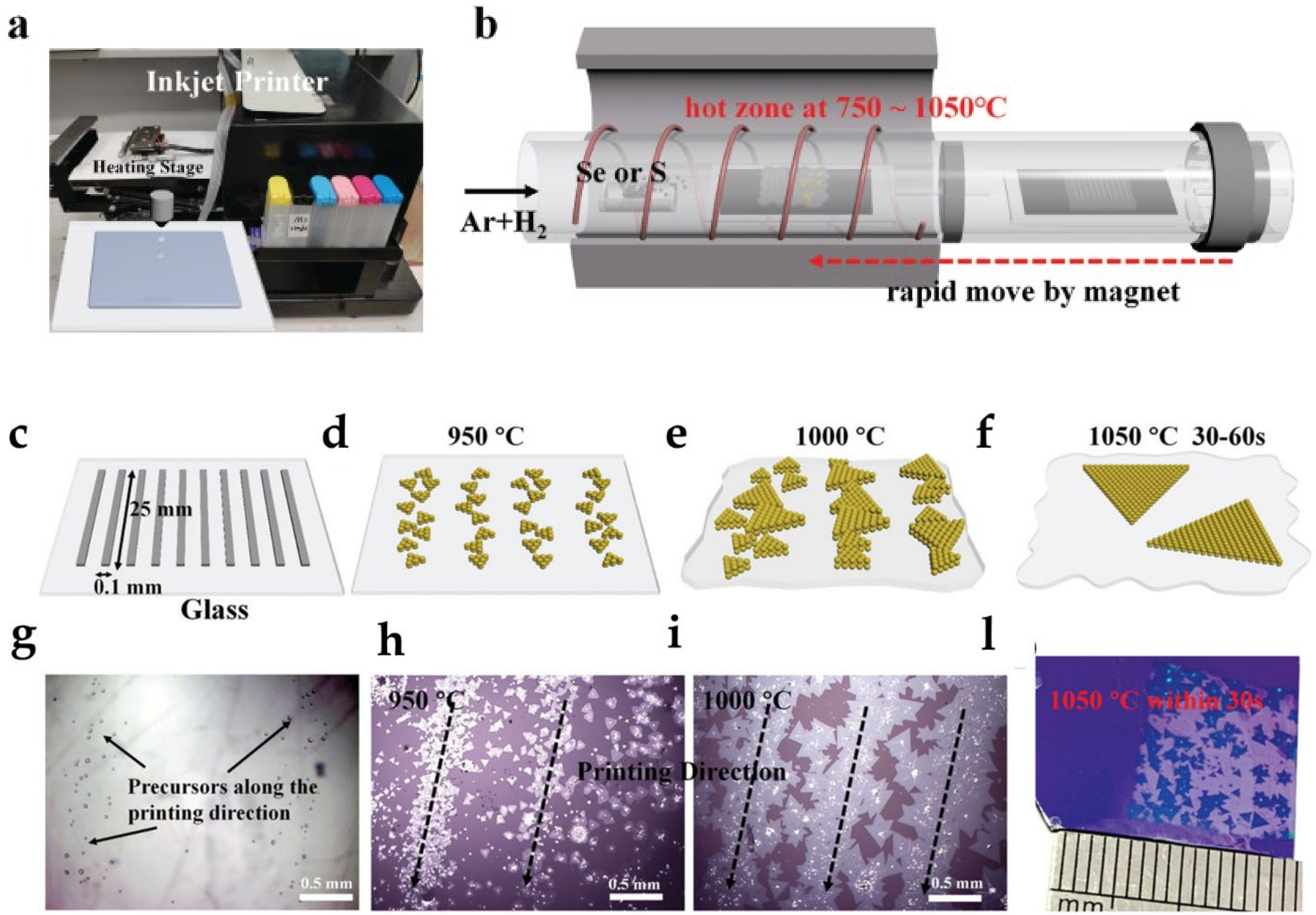
Other metal seeds proven as very valuable for the spatial control of the nucleation of flakes include Pt/Ti and Au [61,62,63]. More recently, the synthesis of patterned MoS2 nanoflakes using an industrial inkjet fed with an aqueous solution of ammonium molybdate tetrahydrate as liquid precursor was demonstrated (Figure 3). The possibility of obtaining large-area patterned 2D films in centimetre size with good controllability of the thickness and good reproducibility opens up interesting possibilities for the development of complex devices based on this material [64].
4. Precursors for MoS2 Growth
The literature has reported the use of several kinds of Mo and S precursors for the CVD growth of MoS2. It is possible to divide these precursors into three main categories according to their physical status: solid, liquid, and gaseous. To optimize the synthesis process and to obtain good control over the number of layers, it is important to understand the limits, advantages, and chemical and physical properties of each precursor. Moreover, for some precursors, several safety issues should be considered. In the following paragraphs, a brief description of the available precursors for each category is given.
5. Solid Precursors
Mo and S powders are still the precursors of choice for many groups to deposit mono- and few-layer MoS2, although the reproducibility of the process remains an issue. This approach is very simple, since the handling of powders is easy, has few hazard problems, and nevertheless permits obtaining high quality flakes. The drawback is that the flake dimension is somewhat limited to some tens of microns; scalability to large areas and enlargement of the single flake are quite difficult, and reproducibility remains an issue.
5.1. Molybdenum
The most commonly used powders for molybdenum are MoO3, available in high purity (99.98%). The vapour pressure of MoO3 was reported in [65]. A quantity of 10–200 mg of MoO3 powders is placed in a quartz crucible near the substrate in the high temperature zone of the reactor. There are several approaches in positioning the substrate; some groups place the substrate facing down directly above the powders, while others place it facing up immediately after the crucible. It should be noted that some impurities might be present in these solid precursors. Robertson et al. [66] showed that Cr and V atoms were found in CVD grown MoS2, most probably from elements present in solid precursors, causing some charge trapping in the grown 2D material. The issue of unintentional doping is very relevant in 2D materials; in [67], the effect of unintentional carbon doping during CVD was discovered and thoroughly discussed.
Precursors such as molybdenum hexacarbonyl (Mo(CO)6) and molybdenum (V) chloride (MoCl5) are mostly used for ALD and MOVPE. Mo(CO)6 is used with H2O or ozone to deposit thin MoO3 films through ALD, to be sulfurized in a subsequent step. Mo(CO)6 has a vapour pressure of about 0.10–0.15 mbar at room temperature and is very volatile (melting point of 150 °C, boiling point of 156 °C) [68].
Molybdenum (V) chloride (MoCl5) powders were also used to grow MoS2 with S powders [69,70]. However, MoCl5 is air sensitive and toxic, so its use poses more hazards than that of MoO3 powders.
Deposition of a thin Mo layer prior to growth could also be included in the solid precursor category. Electron-beam evaporation or sputtering are used to obtain a very thin and controlled Mo layer on the substrate, which is converted to MoS2 because of the exposure of the surface to S vapours. The final MoS2 layers are dependent on the thickness of the initial Mo layer, so it is important to have very precise control over the metal thickness and good homogeneity. MoO3 deposited by evaporation is an alternative approach to metallic Mo [71], since the oxide has a lower evaporation temperature and is easier to sulfurize.
The use of a Mo metal foil was suggested to obtain large flakes on 6-inch substrates [48]. The foil was placed 10 mm above a soda–lime glass substrate and using a mixture of Ar and O2 as carrier, flakes with later size higher than 400 μmm were obtained. Reactive MoO2 was produced thanks to the oxidation of Mo foil by the O2 carrier, and S powders were used as an S precursor. The dimensions of triangular MoS2 flakes were adjusted by controlling the distance between the Mo foil precursor and the substrate.
5.2. Sulfur
S powders are nontoxic and melt at about 115 °C, evaporating to gaseous sulfur. S vapour pressure is reported in [72] but the amount of precursors present in the vapour phase depends also on the quantity of powder placed in the crucible and on the their dimension: a good practice would be to replace the S in the crucible after each growth in order to increase reproducibility and have a better control of the deposited layers.
S powder with a weight in the range of 0.1–1 g is usually placed upstream in a quartz crucible about 10–15 cm away from the substrate. It is heated at temperatures of about 100–200 °C, and the vapour is delivered to the substrate by the carrier gas. In these conditions, the S vapour pressure is in the range of 10−2 – 1 torr. Since the evaporation of S is quite fast, a common technique to ensure repeatability is to independently heat the S crucible only after the substrate has reached the growth temperature setpoint. Moreover, in order to obtain a continuous supply of precursor during the whole process, the use of two different crucibles placed in different reactor position was suggested [73]. As already discussed above, changing the direction of the carrier gas to deliver the S vapours away from the substrate during the heating process may deliver more consistent results [34].
6. Liquid Precursors
The necessity to overcome the reproducibility and size limitations imposed by the use of powders fostered the research of alternative precursors. The idea of sulfurizing a thin and controlled Mo layer deposited on the substrate (originally obtained by sputtering or e-beam) was at the basis of the method of spinning liquid precursors. This approach, well known from the deposition of resists and protective layers, consists of dropping a viscous liquid with the Mo precursor onto the substrate and then using a fast-rotating spinner to spread and homogenize the liquid onto the surface. Once the centripetal and viscous forces are well balanced, the resulting layer has very good thickness reproducibility. Then, the substrate is placed in the reactor chamber and sulfurized using standard S powders.
6.1. Molybdenum
The literature has reported the use of two liquid precursors, sodium molybdate dihydrate (SMD—Na₂MoO₄·2H₂O) and ammonium molybdate tetrahydrate (AMT—(NH4)6Mo7O24). It is important to remember that SMD is incompatible with alkali metals, most common metals, and oxidizing agents. These precursors are usually diluted in water (0.1–0.2 g in 10–50 mL of H2O) and mixed with a promoter such as NaOH (0.1 g in 50 mL of H2O) and a density gradient medium such as iodixanol (Opti-Prep) to facilitate the spinning and substrate adhesion process. Standard proportions for these three components are in the range 1:(1–8):0.5, and they are then spun onto the substate for 30–60 s at 2000–4000 revolutions per minute. An hydrophilic surface is required to obtain a uniform coating molybdenum precursor, so the substrate is usually treated with O2 plasma and/or sodium hydroxide before the drop-casting of the solution [74].
SMD was also used in an alternative approach by embedding it into two thin pieces of glass that were fused together after heating. Thanks to the high temperature, the SMD melted and diffused through the molten glass to its surface with a dissolution–precipitation process. When the metal source reached the upper surface, it reacted with sulfur to grow MoS2 on the molten glass surface. Through this original method, highly uniform and monolayer MoS2 flakes on centimetre-scale glass substrates were obtained thanks to a uniform distribution of the metal precursor [75].
The liquid-phase precursor approach was used to obtain controlled doping of TMD and related heterostructures. Mixing of Mo liquid precursors along with selected dopants (Fe, Re, V) was reported to produce controllable doping in MoS2 with excellent uniformity. More complex structures, such as V-doped in-plane WxMo1−xS2/MoxW1−xS2, were also obtained [76]. Liquid, metal-organic-like precursors are still not common for MoS2 synthesis. Efforts are being directed towards developing suitable reagents to be used in MOCVD systems, in order to enhance process reproducibility and controllability. A notable effort was directed towards bis(tertbutylimido)bis(dimethylamido)molybdenum (Nt Bu)2(NMe2)2Mo, which was stored in a container kept at 45 °C and used as molybdenum precursor with H2S the as sulfurizing agent. A rapid and scalable process using a CVD approach on 2-inch sapphire substrate was developed to synthesize, layer-by-layer, atomically thin MoS2 films with good spatial homogeneity and wafer-scale uniformity [77].
6.2. Sulfur
Dimethyl disulfide (CH3SSCH3, DMDS) is an organic, flammable liquid with a garlic-like odour that can be used as a S precursor. It decomposes into methanethiol (CH3SH), ethene (CH2=CH2), carbon disulfide (CS2), and H2S. Reaction by-products of this precursor pose some safety hazards (see the following section) [78].
Dodecane-1-thiol (or dodecyl mercaptan, C12H25SH) is a sulfur-containing liquid thiol that can be bubbled and delivered into the reactor by using a carrier gas in order to obtain a precise and uniform concentration of S during the process [79].
7. Gaseous Precursors
Sulfur
Despite its toxicity, hydrogen sulfide (H2S) has been used by some groups as a precursor for S. It decomposes very quickly at high temperature, and for this reason, it should be more efficient than S powder for TMD synthesis [80]. Its partial pressure during a typical TMD growth is in the range 10−1–10−2 [81,82]. H2S may also act as a reducing agent for metal oxides. It should be remembered that H2S is also corrosive, flammable, and explosive, with severe consequences in the event of exposure to eyes and skin and inhalation, and the design of a reactor with a H2S line should be carefully planned [83]. Despite these drawbacks due to safety reasons, a gas permit can be used to obtain a very controllable precursor supply, which is reflected in the reproducibility of the process.
8. Safety aspects of Mo and S Precursors
Ingestion of Mo or S related compounds is considered a very unlikely event in a research laboratory if standard precautions for the manipulation of substances are taken into consideration (e.g., wearing gloves, washing hands, etc.). However, it should be taken into consideration that a low level of Mo or S vapours could be present in the ambient because of the volatility of these substances at room temperature. Use of a laboratory hood should be always taken into consideration. Exposure to excess levels of Mo has been associated with adverse health outcomes such as respiratory effects following inhalation exposure to molybdenum trioxide, decreases in body weight, kidney damage, decreases in sperm count, and anaemia following oral exposure. A review of human and laboratory animal health effects for Mo can be found in [84]. Oral exposure to sulfur may cause problems in the gastrointestinal tract, central nervous system, kidneys, liver, heart, lungs, blood, and salivary glands. Sulfur has induced skin damage and affected various other tissues (https://www.bibra-information.co.uk/downloads/toxicity-profile-for-sulphur-1990/ Accesed on 12 September 2021). Handling of H2S exhaust could include a bubbler through an aqueous solution of ethylene glycol to dissolve H2S before releasing it to the atmosphere.
9. The Use of Growth Promoters in MoS2 Synthesis
The growth of 2D layers is driven by the chemical potentials and surface energies of the material and substrate. Depending on the balance between adhesion to the surface of atoms and adatom cohesive force, 2D layer growth might be favoured with respect to island nucleation. If the surface adhesion is insufficient to allow layer growth, the use of additional molecules (that are not involved in the chemical processes underlying the growth) is an attractive method to obtain 2D layers. These elements are generally known as “promoters”, and their use has been proven to be very beneficial for many aspects of the growth of MoS2.
The inclusion of other elements that may favour the nucleation and lateral growth of 2D layers was recognized as crucial in the very early steps of the research on the CVD growth of this material. In particular, the pioneering work of Ling et al. [85] analysed many possible options for promoters, giving an ample view of the possibilities; this was a fundamental paper to have a wide insight on many possible substances to be used as promoters. We limit our discussion to the most successful and useful promoters reported so far, to allow the reader a general view of the state of the art on this topic (Table 1). Many approaches have been proposed in these years, and we consider it useful to divide growth promoters into two main categories: inorganic solid state and organic. A section on the effect of surface treatments is also included, as this is another important element in determining the quality of the grown 2D layers.
From the point of view of understanding the mechanisms underlying the effects of promoters, theoretical work is currently underway, with different proposals to be investigated. For example, in [86], the effect of alkali metal compounds as promoters was studied, and the authors provided an explanation based on eutectic intermediates containing alkali metal molybdates and molybdenum oxides. Because of their low melting point, their mobility was enhanced in comparison with that of other molybdenum compounds, reducing the nucleation of new nanoislands and favouring lateral growth of existing ones.

Table 1.
Growth promoters for the synthesis of MoS2.
| Seeding Promoter | Method | Substrate/Surface | Growth Temperature (°C) | Reference |
|---|---|---|---|---|
| Organic | ||||
| PTAS | dispersed on different substrate | SiO2/Si | >600 | [85] |
| PTAS | dispersed as solution on growth substrate | SiO2/Si, quartz, sapphire, TiO2 | 650–680 | [87,88,89] |
| PTAS | solution drop-casted on oxone-treated surface | graphene | - | [54] |
| PTAS | solution drop-casted on surface at 90 °C | SiO2/Si | 750 | [90] |
| PTARG | solution drop-casted on surface at 90 °C | SiO2/Si | 750 | [90] |
| F16CuPc | prior thermal evaporation on the growth substrate | SiO2/Si | 650 | [85] |
| PTCDA | solution drop-casted on surface | SiO2/Si, sapphire | 650 | [91] |
| PTCDA | solution dispersed on different substrate downstream | SiO2/Si | 750 | [92] |
| rGO | hydrazine solution drop-casted on surface | SiO2/Si, sapphire | 650 | [91] |
| CuPc | solution drop-casted on surface | SiO2/Si | 680 | [85,88] |
| CV (crystal violet) | solution drop-casted on surface | SiO2/Si | 680 | [88,93] |
| H2TPP (porphyrin) | thermal evaporation of thin film | SiO2/Si coated with carbon nanotubes | - | [94] |
| p-THPP | fibres dipped in promoter solution | graphene oxide fibres | 650 | [95] |
| Zn(II)-THPP | metalation of pTHPP promoter | graphene oxide fibres | 650 | [95] |
| Inorganic | ||||
| NaOH | added in liquid precursor solution | SiO2/Si | 780 | [96] |
| NaCl | on substrate facing the growth substrate | SiO2/Si | 750 | [97] |
| NaCl | mixed with solid Mo precursor | SiO2/Si, sapphire, Si, fused quartz, mica | 650 | [50] |
| Alkali metal halides (NaCl, KI) | placed upstream to growth substrate | sapphire | 800 | [98] |
| IIa metal chlorides (CaCl2, SrCl2) | spin-coating of solution on substrate | SiO2/Si, sapphire | 850 | [35] |
| Gold | EBL-patterned arrays of Au nanoparticles | SiO2/Si | 650 | [62] |
| Gold | drop-casting on colloidal Au nanoparticles | SiO2/Si | 785 | [63] |
9.1. Inorganic Solid State Promoters
Among the promoters in this category, sodium was the first and most studied, as its beneficial effects on the lateral growth of flakes were recognized very early. The presence of Na on the substrate acts as a promoter for MoS2 flake nucleation. Moreover, the presence of Na facilitates the peeling of flakes, because it has a low energy barrier between MoS2 and the substrate during the growth process. This permits covering the flakes with a PMMA layer and then detaching the PMMA with the flakes with a simple immersion in water [48]. Na has been used in solution as sodium hydroxide (NaOH), particularly when liquid precursors were used, as it can be easily added to the solution to be spun on the substrate [96].
Another substance containing sodium that has shown usefulness in growing 2D materials is sodium chloride (NaCl). In particular, its use allowed obtaining high-quality MoS2–WS2 in-plane heterostructures [97]. NaCl’s role is related to the enhanced formation of micrometre-sized particles at lower temperature and to the weakening of interlayer adhesion, allowing for the lateral growth of materials. Different processes have been proposed for the role of NaCl, such as: (i) the formation of low-melting-point intermediates, which facilitates a sufficient supply of metal precursors; (ii) the decrease in the energy barrier for atom bonding at the edges of 2D flakes; and (iii) the generation of low-melting point-eutectic intermediates, increasing the surface mobility of precursors [35]. The beneficial effect of mixing NaCl into the MoO3 solid precursors was studied in [50], where 2D flakes were deposited on a variety of substrates. The authors indicated that the inclusion of NaCl allowed for a reduction in the growth temperature from 900 to 650 °C, making it a cost-effective growth promoter for high-quality, large-area monolayer flakes. In [99], the use of this salt was instrumental in obtaining large-area 2D layers of a large series of metal chalcogenides, including MoS2. The authors stated that NaCl helped in reducing the melting points of metal precursors and in increasing the chemical reaction rate to grow 2D TMCs.
In [98], alkali metal halides such as KI and NaCl were considered, highlighting their beneficial effect to the growth of MoS2 nanoflakes, which was due to the suppression of the nucleation of new MoS2 domains during growth and during subsequent enhancement of lateral growth of existing domains. In [100], the role of salts in promoting the 2D growth was interpreted as due to: (i) reaction between alkali metal salts with transition metal precursors forming nonvolatile liquid alkali metal molybdates that reduced the nucleation density and promoted lateral growth; (ii) catalytic effects that increased the surface reaction rate; (iii) the formation of highly active volatile metal oxychlorides possessing relatively low evaporation temperatures; and (iv) reduction in the activation energy on the specific surfaces of nonlayered materials hindering perpendicular growth.
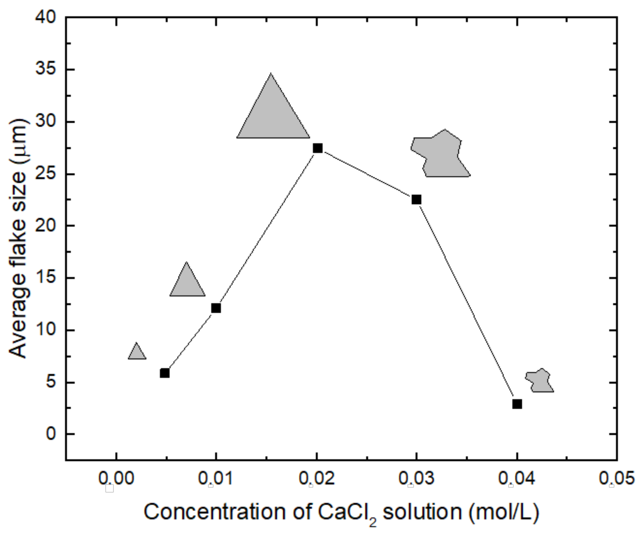
Recently, the use of some group IIA metal chlorides (CaCl2 and SrCl2) as promoters was proposed [35], as it resulted in a relevant increase in the size of flakes, as shown in Figure 4. As in other cases, this promoter was spin-coated on the surface of the substrate as an aqueous solution, while the Mo and S precursors were in solid state. In this comprehensive work, different metal elements (Li, Na, Sr, Mg, Ca) were considered and an acid–base model was developed, allowing the authors to attribute the promoting effect to acid–base interactions between precursors and substrates influencing the adsorption of atoms for the formation of the 2D material.
Beneficial effects are not limited to these substances, since it has been reported that metals in solid state can also favourably influence the 2D growth of MoS2, as discussed above when the use of patterned substrates was introduced. More recently, it was reported that an increase in size of MoS2 flakes occurred after drop-casting a solution with colloidal gold nanoparticles [63]. This effect was explained by gold nanoparticles acting as catalytic seeding points for the initial synthesis of the MoS2 monolayer, similarly to what happens in 1D nanowires [101]. This is a topic of very relevant interest, as the integration of metal nanoparticles (such as gold or silver) with 2D nanostructures is very actively researched because of their effectiveness in enhancing and controlling the light-emission properties of these novel materials, allowing for in-depth studies of light–matter interaction in 2D systems [102,103,104].
9.2. Organic Promoters
Among the most-used organic promoters, perylene-3,4,9,10-tetracarboxylic acid tetrapotassium salt (PTAS) and perylene-3,4,9,10-tetracarboxylic dianhydride (PTCDA) have provided the most interesting results, thanks to the property of aromatic molecules of increasing the wettability of the growth surface and of lowering the free energy for nucleation. The first report on the usefulness of treating surfaces with such substances in obtaining large-area, high-quality TMD materials dates to 2012, when Y.H. Lee et al. used PTAS, PTCDA, and reduced graphene oxide (rGO) [91].
PTAS can be obtained by alkaline hydrolysis of PTCDA by diluting it in ethanol and adding KOH aqueous solution while refluxing. Ethyl ether can be added dropwise to the solution until a solid product begins to separate out. The precipitate can then be filtered and dissolved in deionized water, and the obtained aqueous solution must be filtered again to remove any insoluble residuals. Adding ethanol to the resulting aqueous filtrate allows precipitating the PTAS final product [105].
In a later study, Ling et al. [85] showed that PTAS permitted the growth of good-quality MoS2 monolayers at 650 °C, while the use of PTCDA allowed the use of lower temperatures while maintaining good quality in the nanostructures. As illustrated in Figure 5, when the promoter is deposited on a different substrate with respect of the growth one, the diffusion of the seeding molecules causes a concentration gradient from the promoter substrate over to the growth region.
The use of PTAS was recently demonstrated as very effective in achieving lateral heterostructures wherein MoS2 and other 2D materials can be parallel stitched [106]. Ref. [89] provided the possible growth mechanisms underlying the growth of nanoflakes, showing that this 2D material could be obtained on different surfaces such as Si particles, TiO2 aggregates, and quartz.
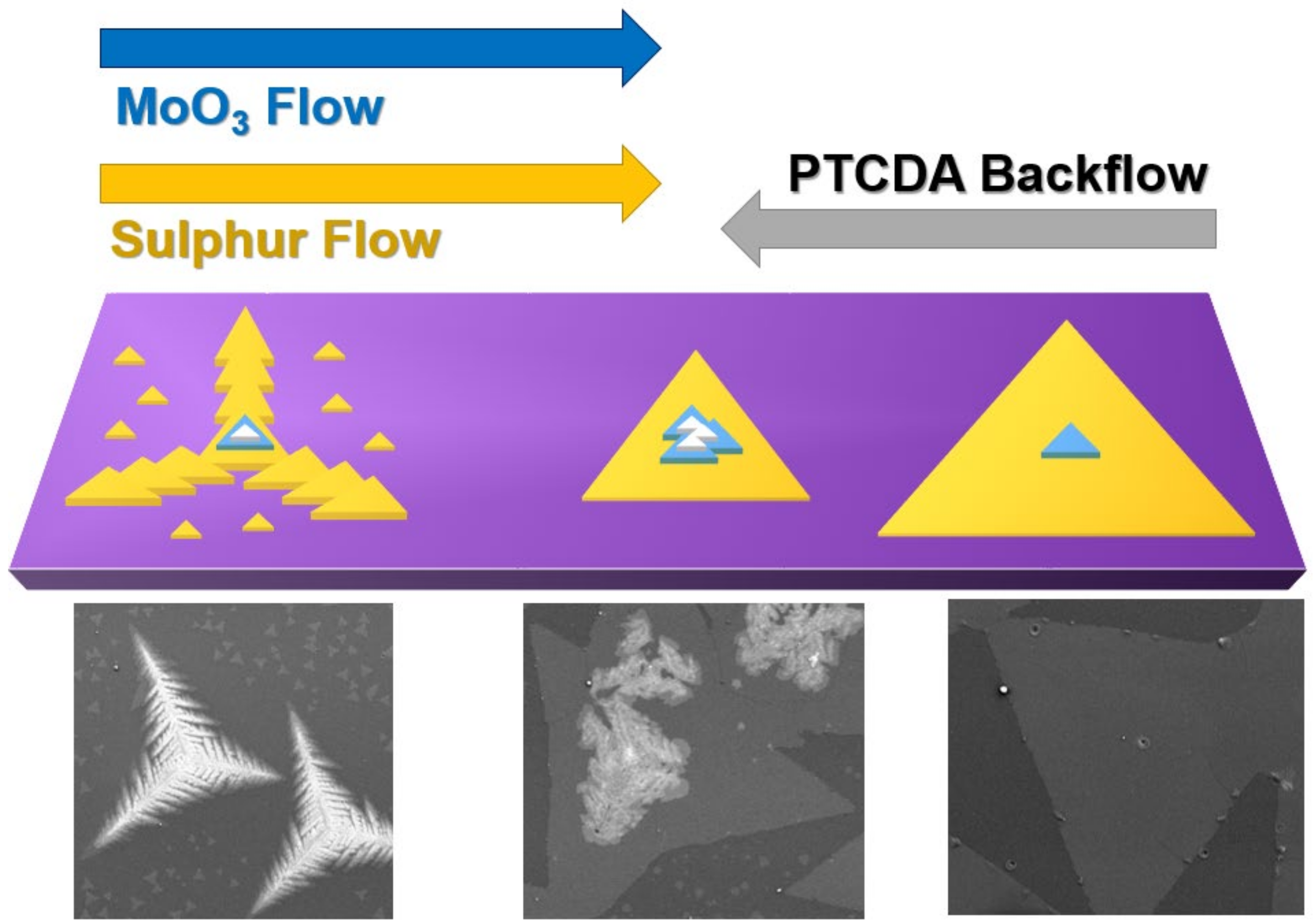
In [92], the effect of gradient of PTCDA on the growth dynamics was clarified, highlighting that a low amount of this organic promoter led to reduced lateral growth and boosted vertical growth, while a high amount enhanced lateral growth and suppressed vertical growth. Figure 6 illustrates the proposed growth dynamics due to the two opposite flows of precursors and PCTDA. This configuration allowed studying the effect of the gradient of this organic promoter on the MoS2 structure morphology and flake sizes along the length of the growth substrate.
As was shown recently by Martella et al. [91], the use of organic promoters can also be useful for tailoring the properties of 2D structures. Using two different perylene-based molecules (PTAS and perylene-3,4,9,10-tetracarboxylic dianhydride—PTARG) as seeding promoters resulted in a change in the local electronic polarizability of MoS2 monolayers due to extra charges trapped in the MoS2 monolayers.
Copper phthalocyanine (CuPc) and copper(II)-hexadecafluoro-29H,31H-phthalocyanine (F16CuPc) have also given interesting results [85,88], with performance comparable to PTAS and PTCDA in facilitating the growth of large-area, high-quality, and uniform monolayer and few-layer flakes. F16CuPc has the attractive property of high stability at high temperature, making this a good choice for high-temperature growth processes.
Another interesting organic compound is crystal violet (CV), thanks to the possibility of engineering its configuration by simply varying the polarity of solvent of the solution. Ko et al. [93] studied the effects of different CV conditions on the growth of MoS2 nanoflakes both from an experimental and a theoretical perspective. Their results gave interesting insight on the growth of monolayer MoS2 from aromatic seeding promoters.
Thin films of 5, 10, 15, 20-tetraphenylporphyrin (H2TPP) were used as a promoter layer for the realization of hybrid structures composed of carbon nanotubes and MoS2 nanosheets for the realization of flexible chemical sensors [94] and for the growth of vertical MoS2 nanosheets [107]. The use of this promoter also allows for the simultaneous doping of the material by performing a metalation of the H2TPP films, obtaining different metalloporphyrins such as Al(III)-tetraphenyl porphyrin (Al(III)TPP) or Zn(II) meso-tetra(4-hydroxyphenyl) porphyrin (Zn(II)THPP) [108]. Porphyrin-based organic molecules such as 5,10,15,20-tetrakis(4-hydroxyphenyl)-21H,23H-porphyrin (p-THPP) were used also for the growth of MoS2 on graphene oxide fibres. In [95], these fibres were dipped in the promoter solution. The use of Zn(II)THPP to achieve zinc-doping of the flakes was also demonstrated.
9.3. Surface Treatments
In their pioneering work, van der Zande et al. [26] showed that a careful treatment of SiO2/Si substrates (2 h in H2SO4/H2O2 (3:1) followed by 5 min of O2 plasma) and a minimal exposure of the precursors to air during storage was sufficient to obtain large flakes up to 100 µm. From these experimental observations, it is evident that the state of the surface on which the growth is carried on is of paramount relevance for the quality of flakes. From this point of view, many approaches to optimize this surface have been studied in the past. For example, the treatment of SiO2/Si substrates with oxygen plasma resulted in layer-controlled and large-area CVD MoS2 films [109].
Another interesting approach was studied recently that relied on the treatment of the SiO2 substrate by a piranha etching solution prior to deposition. The authors stated that this treatment reduced the surface free energy of the substrate, making the use of promoters unnecessary [110]. An interesting method to treat surfaces to ease the transfer of flakes was proposed by Shinde et al. [111]. By etching an SiO2 surface with hydrofluoric acid, the hydrophilicity is increased, allowing water to penetrate at the interface between polymer-capped MoS2 and the substrate, resulting in direct transfer of flakes over a large area.
10. Growth Mechanisms
The synthesis of MoS2 by CVD is the result of several steps, which can be summarized as follows: (i) transport of precursors to the substrate by a carrier gas; (ii) diffusion through the boundary layer from the gas phase to the substrate surface; (iii) adsorption of molecules to the substrate surface; (iv) diffusion of adsorbed molecules on the surface; (v) heterogeneous reactions on the surface resulting in TMD growth; (vi) desorption of by-products. In order to control the process and obtain a monolayer or few-layer material as an outcome, a high degree of control of the heterogeneous reactions should be pursued [35]. The exact evolution and progress of the synthesis and its mechanisms depend, of course, on the chosen precursors. The “holy grail” of MoS2 CVD would be to develop a precise, controllable, and reproducible process to uniformly deposit large-area monodimensional flakes over a large area without grain boundaries and with a low density of defects. Understanding the growth mechanisms for the different available precursors and considering the possible presence of growth promoters could help to recognize the strengths and weaknesses of these precursors.
Considering the experience gathered on graphene, but at the same keeping in mind that the synthesis of MoS2 proceeds through completely different mechanisms, in order to promote the growth of large 2D flakes, it is important to decrease the density of the nuclei and to increase the lateral growth rate while at the same time suppressing 3D nucleation [112]. Nucleation of MoO3−x species at the beginning of growth is the first step to allow the formation of MoS2 nanoparticles and large flakes in the later stage of the synthesis [113]. It was suggested that this growth mode is essentially controlled by the deposition rate, which should be kept below a certain threshold to avoid the formation of thicker islands. Kang et al. [32] observed that this occurred when a low partial pressure of Mo vapour was used. With a higher Mo partial pressure, the layer-by-layer growth mode was abandoned in favour of the nucleation of a mixture of monolayer, multilayer, and no-growth regions. To obtain uniform monolayer growth, potentially on a large substrate, a precise and constant Mo partial pressure for the entire duration of growth is necessary. This requirement is not straightforward when Mo powders are used as precursors, since they deplete and are consumed as the growth proceeds, but is more easily obtained using metal-organic-like precursors such as Mo(CO)6.
The competition between the precursor mass flow towards the substrate and the reactions occurring at the surface determines the ultimate evolution of the growth. Zhou et al. [114] presented a general growth model for the deposition of a wide variety of TMDs, combining 12 transition metals and 3 chalcogens to synthesize up to 47 different 2D materials. They suggested that the mass flow supply determines the amount of metal precursors involved in the formation of the nucleus and the growth of domains, while the growth rate, essentially determined by the temperature, dominates the grain size of the layer. The interplay between growth rate and mass flow determines the formation of continuous monolayers, small flakes, atomic clusters, or large 2D single crystals. The two contradictory statements presented in [32,114] may be interpreted as a sign that the deposition of MoS2 with powders is very dependent on the used growth system and setup, and finding a unifying explanation of the experimental observation is not straightforward.
The main reason for the lateral enlargement of MoS2 flakes is the high chemical reactivity of the atoms at the edge of the flakes and in the presence of preferred nucleation sites, with high chemical reactivity, compared to the absence of dangling bonds in the vertical direction. A low and constant Mo precursor partial pressure may help in growing uniform monolayer thin films over a large area [32]. However, the growth of vertically standing MoS2 nanosheets was also reported [115]. They were supposed to be caused by the reduction in the elastic strain energy that forms during the horizontal growth of MoS2 nanosheets. The transition from 2D to 3D structure was achieved by controlling the quantity and distribution of the precursor concentration, placing the substrate in different orientations and positions with respect to the source powders [107]
When using Mo powders, the proposed reactions for MoS2 synthesis are:
2 MoO3 + S → 2 MoO3−x + SO2
2 MoO3−x + (7 − x) S → 2 MoS2 + (3 − x) SO2
MoO3 is first reduced to suboxides (MoO3−x) by S vapours, further reduced to oxisulfides, and then transported to the substrate, where a further reaction with S vapour to form MoS2 occurs [116]. Since a MoO3 suboxide is involved in the growth reaction, the use of MoO2 instead of MoO3 was proposed in order to obtain better control of the flakes [117]. In this case, the synthesis reaction would proceed by the mechanism:
MoO2 + 3 S → MoS2 + O2
This reaction avoids intermediate chemistry and permits obtaining higher-quality flakes on different substrates such as SiO2, Si, quartz, and SiN. The quantity of starting Mo powders greatly influences the reaction process. In [118], a comprehensive summary of typical powder weights, along with growth temperature and setup, was presented.
In order to have a detailed outlook on the growth process of MoS2, Cain et al. [119] deposited MoS2 using S and MoO3 powders on ultrathin SiO2 membranes to allow investigation of the nucleation mechanism with aberration-corrected STEM and elemental EDS mapping. They confirmed the presence of nucleation centres (10–30 nm) only at the centres of triangular flakes, representing the early stages of TMD growth. The second or third layer of the flakes also started at this site. Moreover, the nuclei showed a nanoscale core–shell structure, similar to that of inorganic TMD fullerenes, with inhomogeneous distribution of Mo and S. The growth process was essentially defined by the concentration of the chalcogen vapour: if the atmosphere was weakly reducing (sulfur poor), oxi-chalcogenide particles with an orthorhombic crystal structure were formed. In a moderately reducing sulfur-rich atmosphere, MoS2 formation was favoured. These experimental observations confirm the importance of promoting the formation of nucleation sites.
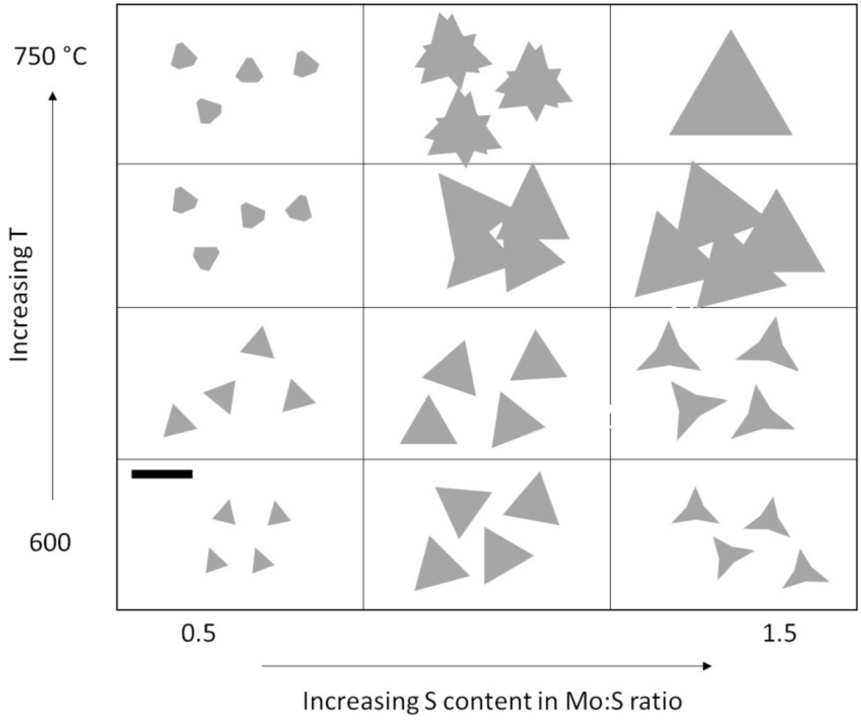
A convenient and empirical method to tune growth parameters towards the optimal growth conditions is to observe the flake shape at the optical microscope. Yang et al. [120] studied the morphological evolution of MoS2 flakes for various Mo–S ratios, using MoO3 and S powders as reagents at different temperatures. Obtaining a continuous film with large triangular MoS2 flakes should be possible at higher temperature and with a high S content (Figure 7).
Obtaining large flakes, by preventing the cohesion of smaller flakes, would also limit the presence of grain boundaries at flake coalescence regions, which may limit electrical transport in the layer [16]. Moreover, it was observed that the MoS2 bandgap could be tuned by controlling the distance from a grain boundary [121], so it is important to achieve good control over the flakes’ size over the substrate area in order to avoid undesired modulations of the bandgap. Nevertheless, it was demonstrated that MoS2 grain boundaries could exhibit a memristor behaviour [122], which may open new applications for this material.
An important source of carrier scattering in devices is defects and charged particles at the interface (Coulomb scattering). These defects are usually introduced in postprocessing fabrication steps, and it was suggested that proper passivation with a suitable dielectric could help mitigating the issue, increasing the performance of the device [123].
In general, point defects in MoS2 act as important electron scattering centres and may be categorized as vacancies or antisite defects [124,125]. Sulfur vacancies behave as deep donors and induce midgap defect states, making the material n-type. Furthermore, vacancies and antisites induce a modification in the electrical properties of MoS2, resulting in n-type doping and introducing localized states in the band gap, lowering the carrier mobility. They can cause Fermi level pinning and high contact resistance in electrical devices. Inclusion of other elements related to promoters (Na, Au) can also cause unintentional doping effects. These states also reduce the emission efficiency for photonic devices based on this material.
On the other hand, control of defect density and nature can be an effective tool to engineer material properties. It was shown that the electrical properties of MoS2 could be changed by exposing the samples to oxygen plasma, going from the semiconducting to the insulating regime [50]. A recent method to reduce sulfur vacancies was introduced by Durairaj et al. [126]; in this study, a SiO2/Si wafer was placed next to the growth substrate, providing oxygen and effectively enabling oxygen passivation of sulfur-vacancy defects in monolayer flakes. The authors observed a threefold increase in the PL efficiency due to the elimination of defect-related bound exciton emission.
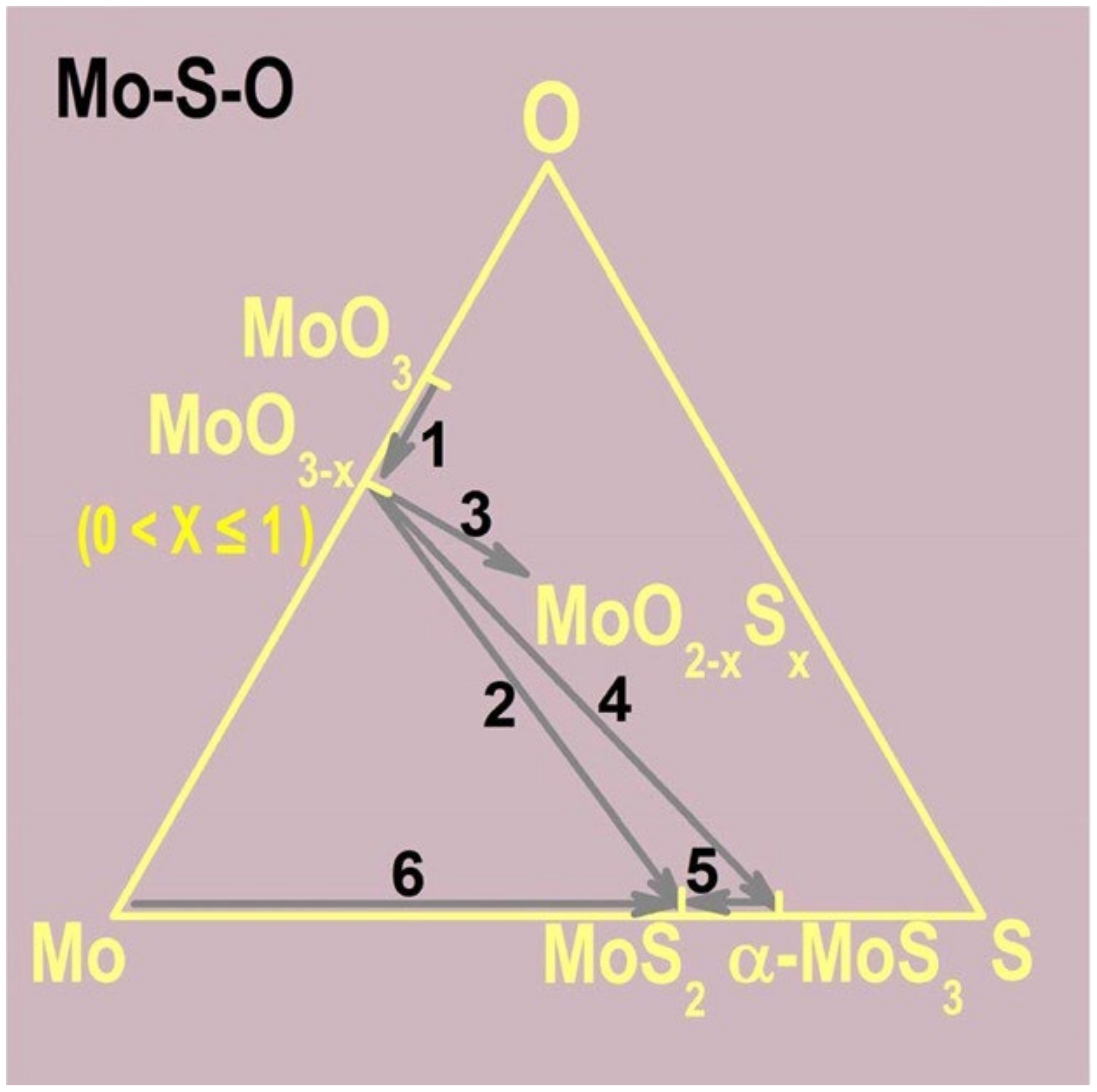
In Figure 8, the reaction pathways that lead to the formation of MoS2 through intermediate species are summarized [118,127].
If MoCl5 is used instead of MoO3 powders, the proposed reactions are different from those reported above. Since the ratio between S and MoCl5 is very high (>1000), the conversion of MoCl5 to MoS2 is supposed to be completed in the gas phase, with a negligible concentration of intermediate suboxides. By precisely controlling the amounts of MoCl5 and S powders, their flow in the growth environment, and the total pressure in the growth chamber, Yu et al. [69] were able to control the number of MoS2 layers, with good uniformity over an area of several cm2. The key role was suggested to be the self-limiting nature of the layer-by-layer process, which could be controlled by tuning the flow of the precursors as well as the total pressure of the system: increasing the amount of precursors (from 1 mg of MoCl5 to 25 mg) and the total pressure (from 2 to 750 torr) resulted in the deposition of thicker films.
One could argue that the use of powder Mo precursors, because of their time-dependent evaporation and the necessity of precise and continuous flow control, would lead to worse and less reproducible results with respect to the sulfurization of a thin Mo layer predeposited on the substrate [118]. In the latter case, the resulting MoS2 layer would depend only on the starting conditions, which in principle could be precisely optimized by thermal evaporation or sputtering of the thin Mo or MoOx layer. However, starting with a Mo film deposited on the substrate, the sulfurization process should occur at very high temperature to be efficient. This results in undesired surface evaporation of the starting material and leads to inhomogeneities, since the balance between the surface mobility and surface evaporation leads to limited grain sizes and/or limited yields of monolayer films. Moreover, it is still difficult to obtain an optimal starting film density and uniformity. However, one of the advantages of this approach is the ease of saturating the growth chamber with sulfur vapours (either from powders or from H2S), so this is not the process-limiting factor.
To promote bilayer growth, the interactions between the adatoms and the surface should be larger than the adatom–adatom interactions. If these conditions are not met, the deposition evolves towards a 3D growth. It was suggested that by increasing the intermolecular acid–base interactions between admolecules and the substrate surface, it should be possible to increase the adsorption. This can be done by selecting precursors and substrates with complementary acid/base properties [35]. A convenient way to increase the surface forces is to use growth promoters or seed molecules to change the surface energy, reduce the free energy barrier, and lower the nucleation energy necessary to obtain monolayer MoS2. It was argued that the best promoters are aromatic or graphene-like molecules that enhance the wettability of the substrate, lowering the free energy for the nucleation. In this way, better control of nucleation can be achieved [91]. Thus, an optimal concentration of the seeding promoter is essential for MoS2 monolayer deposition [128]. One important factor to be considered is the polarity of the growth promoter molecule, as pointed out by Ko et al. [93]. With density function theory calculations coupled to experimental evidence, they suggested that the polar part of the crystal violet molecule used as a promoter provides a preferred site for S adsorption, initiating the MoS2 nucleation. The orientation of the molecule during the spinning on the substrate, mediated by appropriate solvents, can effectively promote monolayer growth instead of multilayer MoS2 deposition.
It has been shown that the use of alkali-based promoters allows for larger flakes [98], but their excess might result in loss of MoS2 crystallinity, with the creation of additional defects [128]. Extensive work is currently underway on controlling defects in MoS2 flakes acting on growth parameters, not only to reduce their deleterious effects on devices, but also to take advantage of some of their features. For example, Na cations coming from promoters can cure interface defects to achieve low intrinsic defect levels and enhance electrical properties [129]. The use of liquid precursors spun in a controllable way on the substrate could overcome the problems due to the limited supply control of powder precursors. Spinning SMD and/or AMT with a density gradient medium and a growth promoter such as NaOH or NaCl could permit obtaining a reproducible layer that could be sulfurized in a controllable way. Kang et al. [130] presented a comprehensive study on the role of the different growth parameters in the synthesis of MoS2 flakes using liquid precursor, including the roles of temperature, S pressure, gas carrier flow, composition of the initial spun solution, and time. By an optimization of the process, MoS2 flakes with dimensions up to 100 μm were obtained in a reproducible way. AFM analysis of the MoS2 surface revealed the presence of precursor and promoter residues, particularly at the interfaces between different flakes. AMT is converted to MoO3 at about 300 °C. Using Na as a promoter, if further reacts with NaOH to produce sodium molybdate (Na6MoO4), which finally converts to MoS2 thanks to the presence of S vapour. Using SiO2 as a substrate, in this case, permits the reaction between Na2MoO4 and the oxide substrate to form sodium silicon oxide, promoting the lateral growth of the MoS2 layer [97].
11. Conclusions and Outlook
The rising interest in 2D MoS2 comes from its peculiar physical, chemical, and mechanical properties, including, among other features, peculiar light adsorption characteristics and promising electrical transport properties.
However, the synthesis of reproducible, uniform, and single-layer MoS2 flakes on large-area wafers is still a challenge, and open issues remain to be solved. Increasing control of the deposition process is mandatory to fine-tune the electrical and optical properties of MoS2. At the same time, obtaining flakes with larger dimensions, higher density, and a low concentration of defects is necessary to pave the way for the industrial application of this material. In this review, we explore the CVD synthesis of mono- and few-layer MoS2, giving an overview of the growth method, different substrates for deposition, and the used precursors and growth promoters. The topic of the doping of this material is also considered, and different growth mechanisms involving different types of precursors are overviewed.
From the critical analysis of the results obtained so far, it emerged that homogenous precursor feed, and in particular the achievement of fine control of Molybdenum supply during the CVD process, are necessary conditions for the optimization of the process. Because of their ease of use, the most used precursors for MoS2 synthesis are still Mo and S powders, but this approach presents several issues, such as poor control of the precursor supply causing low reproducibility. The use of growth promoters has allowed overcoming these problems, but the process is far from being optimized for an industrial scale-up. A more recent approach involves the use of liquid precursor spun on the substrate to obtain a controllable thin layer containing Mo and Na as promoter. This method permitted overcoming the problems faced by the other techniques to increase the reproducibility and yield of the process, resulting in very large flakes on very wide areas.
The vast majority of the CVD reactors used for MoS2 deposition have a horizontal geometry, which is known to have intrinsic flow inhomogeneities due to precursor depletion. This may be among the causes of the generally low reproducibility often observed in standard setups. Switching to a vertical gas distribution may help to solve these issues and obtain a better run-to-run consistency.
It is well known that CVD protocols are not easily transferrable from one laboratory to another, as even minimal changes in reactor parameters and growth conditions strongly affect reproducibility of the growth of 2D materials. It seems that many processes and recipes presented in literature worked only in a specific growth setup and configuration. There is a need to identify universal conditions and reaction schemes that will permit better control of the deposition of 2D MoS2 flakes. For this reason, further work on the theoretical modelling of growth is urgently needed to help identify the most crucial parameters. More experimental efforts focusing on the effects of other parameters somewhat overlooked (sulfur partial pressure, carrier gas flows, reactor geometry, and size) could also be useful to gain more knowledge.
From the point of view of reproducibility, the use of liquid precursors seems to have some advantages, as it allows a more precise and reproducible control of the amount of Mo source materials. Similarly, the use of sulfur powders is a crucial element, as the quantity of vapourized sulfur also depends on the mass of powder put in the crucible. The use of sulfur gas has shown some advantages, despite its safety drawbacks. Also, the precise control of gas flows is a fundamental parameter to achieve reproducibility of results.
In our opinion, high-quality, large flakes can be obtained in a controllable and reproducible way using a combination of these three fundamental elements: (i) liquid precursors, (ii) controlled surface treatments (etching and/or plasma), and (iii) organic promoters (Na-based ones being the most effective). However, the optimal combination of these elements has still not been clearly identified, and exact protocols and recipes are still very cumbersome; more research work is needed to identify the optimal conditions.
From the work presented in the literature, it seems that the uniformity of large flakes is strongly dependent on the state of the growing surface. Reduced graphene and sapphire seem to have an advantage, but by careful etching and cleaning of the substrate (by methods such as plasma cleaning), very good results can be obtained also on more common and less expensive systems such as SiO2/Si. These excellent results are fostering a large increase in studies and activities on the growth of this material, considering different substrates on which to grow it, various elements for doping, and the development of reliable models to gain insight on the growth mechanisms. Variations on the basic CVD concepts to achieve better control of precursor supply through various hardware modifications of the apparatus have been proposed with encouraging results.
From this perspective, the knowledge on the CVD growth of MoS2 seems to be mature enough to envision the design and realization of complex heterostructures based on MoS2, in which not only the materials but their dimensionality are different (so-called hybrid heterostructures).
However, we think that at the moment, there is a bottleneck on the realization of complex heterostructures, as the transfer of flakes from one substrate to another is a very complex and delicate step that could represent a second major hurdle for the transfer of the technology for this material to the development of commercial devices. Therefore, it would be desirable to achieve large-area flakes on other substrates, such as metals, semiconductors, and possibly flexible substrates, on which devices can be directly fabricated.
Moreover, we are keen to consider that the next major breakthrough for MoS2 is related to the possibility of realizing patterned deposition of this 2D material, aiming for a method to obtain designed microcircuits. From this point of view, the possibility of “printing” MoS2 layers seems to us a more appealing approach than delicate and cumbersome transfer and manipulation of large flakes.
Author Contributions
Writing—review and editing, L.S. and M.B. All authors have read and agreed to the published version of the manuscript.
Funding
This research received no external funding.
Institutional Review Board Statement
Not applicable.
Informed Consent Statement
Not applicable.
Data Availability Statement
No new data were created or analyzed in this study.
Conflicts of Interest
The authors declare no conflict of interest.
References
- Gupta, D.; Chauhan, V.; Kumar, R. A comprehensive review on synthesis and applications of molybdenum disulfide (MoS2) material: Past and recent developments. Inorg. Chem. Commun. 2020, 121, 108200. [Google Scholar] [CrossRef]
- Zhang, S.; Le, S.T.; Richter, C.A.; Hacker, C.A. Improved contacts to p-type MoS2 transistors by charge-transfer doping and contact engineering. Appl. Phys. Lett. 2019, 115, 73106. [Google Scholar] [CrossRef] [PubMed]
- Abuzaid, H.; Williams, N.X.; Franklin, A.D. How good are 2D transistors? An application-specific benchmarking study. Appl. Phys. Lett. 2021, 118, 30501. [Google Scholar] [CrossRef]
- Wang, H.; Yu, L.; Lee, Y.-H.; Shi, Y.; Hsu, A.; Chin, M.L.; Li, L.-J.; Dubey, M.; Kong, J.; Palacios, T. Integrated Circuits Based on Bilayer MoS2 Transistors. Nano Lett. 2012, 12, 4674–4680. [Google Scholar] [CrossRef] [PubMed] [Green Version]
- Nalwa, H.S. A review of molybdenum disulfide (MoS2) based photodetectors: From ultra-broadband, self-powered to flexible devices. RSC Adv. 2020, 10, 30529–30602. [Google Scholar] [CrossRef]
- Pumera, M.; Loo, A.H. Layered transition-metal dichalcogenides (MoS2 and WS2) for sensing and biosensing. TrAC Trends Anal. Chem. 2014, 61, 49–53. [Google Scholar] [CrossRef]
- Zhu, M.; Du, X.; Liu, S.; Li, J.; Wang, Z.; Ono, T. A review of strain sensors based on two-dimensional molybdenum disulfide. J. Mater. Chem. C 2021, 9, 9083–9101. [Google Scholar] [CrossRef]
- Butun, S.; Tongay, S.; Aydin, K. Enhanced Light Emission from Large-Area Monolayer MoS2 Using Plasmonic Nanodisc Arrays. Nano Lett. 2015, 15, 2700–2704. [Google Scholar] [CrossRef]
- Ponomarev, E.; Gutiérrez-Lezama, I.; Ubrig, N.; Morpurgo, A.F. Ambipolar Light-Emitting Transistors on Chemical Vapor Deposited Monolayer MoS2. Nano Lett. 2015, 15, 8289–8294. [Google Scholar] [CrossRef] [Green Version]
- Golovynskyi, S.; Irfan, I.; Bosi, M.; Seravalli, L.; Datsenko, O.I.; Golovynska, I.; Li, B.; Lin, D.; Qu, J. Exciton and trion in few-layer MoS2: Thickness- and temperature-dependent photoluminescence. Appl. Surf. Sci. 2020, 515, 146033. [Google Scholar] [CrossRef]
- Golovynskyi, S.; Bosi, M.; Seravalli, L.; Li, B. MoS2 two-dimensional quantum dots with weak lateral quantum confinement: Intense exciton and trion photoluminescence. Surfaces Interfaces 2021, 23, 100909. [Google Scholar] [CrossRef]
- Cho, A.-J.; Park, K.C.; Kwon, J.-Y. A high-performance complementary inverter based on transition metal dichalcogenide field-effect transistors. Nanoscale Res. Lett. 2015, 10, 1–6. [Google Scholar] [CrossRef] [PubMed] [Green Version]
- Swain, G.; Sultana, S.; Parida, K. A review on vertical and lateral heterostructures of semiconducting 2D-MoS2 with other 2D materials: A feasible perspective for energy conversion. Nanoscale 2021, 13, 9908–9944. [Google Scholar] [CrossRef] [PubMed]
- Xiao, D.; Liu, G.-B.; Feng, W.; Xu, X.; Yao, W. Coupled Spin and Valley Physics in Monolayers of MoS2 and Other Group-VI Dichalcogenides. Phys. Rev. Lett. 2012, 108, 196802. [Google Scholar] [CrossRef] [Green Version]
- Yu, Z.; Ong, Z.-Y.; Li, S.-L.; Xu, J.; Zhang, G.; Zhang, Y.-W.; Shi, Y.; Wang, X. Analyzing the Carrier Mobility in Transition-Metal Dichalcogenide MoS2 Field-Effect Transistors. Adv. Funct. Mater. 2017, 27. [Google Scholar] [CrossRef] [Green Version]
- Ly, T.H.; Perello, D.J.; Zhao, J.; Deng, Q.; Kim, H.; Han, G.H.; Chae, S.H.; Jeong, H.Y.; Lee, Y.H. Misorientation-angle-dependent electrical transport across molybdenum disulfide grain boundaries. Nat. Commun. 2016, 7, 10426. [Google Scholar] [CrossRef] [Green Version]
- Lin, Y.; Torsi, R.; Geohegan, D.B.; Robinson, J.A.; Xiao, K. Controllable Thin-Film Approaches for Doping and Alloying Transition Metal Dichalcogenides Monolayers. Adv. Sci. 2021, 8, 2004249. [Google Scholar] [CrossRef]
- Rai, A.; Movva, H.C.P.; Roy, A.; Taneja, D.; Chowdhury, S.; Banerjee, S.K. Progress in Contact, Doping and Mobility Engineering of MoS2: An Atomically Thin 2D Semiconductor. Crystals 2018, 8, 316. [Google Scholar] [CrossRef] [Green Version]
- Zhang, K.; Bersch, B.M.; Joshi, J.; Addou, R.; Cormier, C.R.; Zhang, C.; Xu, K.; Briggs, N.C.; Wang, K.; Subramanian, S.; et al. Tuning the Electronic and Photonic Properties of Monolayer MoS2 via In Situ Rhenium Substitutional Doping. Adv. Funct. Mater. 2018, 28, 1706950. [Google Scholar] [CrossRef]
- Xu, E.Z.; Liu, H.M.; Park, K.; Li, Z.; Losovyj, Y.; Starr, M.; Werbianskyj, M.; Fertig, H.A.; Zhang, S.X. p-Type transition-metal doping of large-area MoS2 thin films grown by chemical vapor deposition. Nanoscale 2017, 9, 3576–3584. [Google Scholar] [CrossRef]
- Yang, L.; Majumdar, K.; Liu, H.; Du, Y.; Wu, H.; Hatzistergos, M.; Hung, P.Y.; Tieckelmann, R.; Tsai, W.; Hobbs, C.; et al. Chloride Molecular Doping Technique on 2D Materials: WS2 and MoS. Nano Lett. 2014, 14, 6275–6280. [Google Scholar] [CrossRef] [Green Version]
- Li, M.; Yao, J.; Wu, X.; Zhang, S.; Xing, B.; Niu, X.; Yan, X.; Yu, Y.; Liu, Y.; Wang, Y. P-type Doping in Large-Area Monolayer MoS2 by Chemical Vapor Deposition. ACS Appl. Mater. Interfaces 2020, 12, 6276–6282. [Google Scholar] [CrossRef] [PubMed]
- Zhang, K.; Feng, S.; Wang, J.; Azcatl, A.; Lu, N.; Addou, R.; Wang, N.; Zhou, C.; Lerach, J.; Bojan, V.; et al. Manganese Doping of Monolayer MoS2: The Substrate Is Critical. Nano Lett. 2015, 15, 6586–6591. [Google Scholar] [CrossRef] [PubMed]
- Li, X.; Zhu, H. Two-dimensional MoS2: Properties, preparation, and applications. J. Materiomics 2015, 1, 33–44. [Google Scholar] [CrossRef] [Green Version]
- Mouloua, D.; Kotbi, A.; Deokar, G.; Kaja, K.; El Marssi, M.; EL Khakani, M.; Jouiad, M. Recent Progress in the Synthesis of MoS2 Thin Films for Sensing, Photovoltaic and Plasmonic Applications: A Review. Materials 2021, 14, 3283. [Google Scholar] [CrossRef]
- Van der Zande, A.; Huang, P.; Chenet, D.A.; Berkelbach, T.C.; You, Y.; Lee, G.-H.; Heinz, T.F.; Reichman, D.R.; Muller, D.; Hone, J.C. Grains and grain boundaries in highly crystalline monolayer molybdenum disulphide. Nat. Mater. 2013, 12, 554–561. [Google Scholar] [CrossRef] [PubMed] [Green Version]
- Dumcenco, D.; Ovchinnikov, D.; Marinov, K.; Lazić, P.; Gibertini, M.; Marzari, N.; Sanchez, O.L.; Kung, Y.-C.; Krasnozhon, D.; Chen, M.-W.; et al. Large-Area Epitaxial Monolayer MoS2. ACS Nano 2015, 9, 4611–4620. [Google Scholar] [CrossRef] [PubMed]
- Yang, P.; Yang, H.; Wu, Z.; Liao, F.; Guo, X.; Deng, J.; Xu, Q.; Wang, H.; Sun, J.; Chen, F.; et al. Large-Area Monolayer MoS2 Nanosheets on GaN Substrates for Light-Emitting Diodes and Valley-Spin Electronic Devices. ACS Appl. Nano Mater. 2021, 4, 12127–12136. [Google Scholar] [CrossRef]
- Tang, L.; Li, T.; Luo, Y.; Feng, S.; Cai, Z.; Zhang, H.; Liu, B.; Cheng, H.-M. Vertical Chemical Vapor Deposition Growth of Highly Uniform 2D Transition Metal Dichalcogenides. ACS Nano 2020, 14, 4646–4653. [Google Scholar] [CrossRef]
- Zhang, X.; Ning, J.; Li, X.; Wang, B.; Hao, L.; Liang, M.; Jin, M.; Zhi, L. Hydrogen-induced effects on the CVD growth of high-quality graphene structures. Nanoscale 2013, 5, 8363–8366. [Google Scholar] [CrossRef]
- Li, X.; Li, X.; Zang, X.; Zhu, M.; He, Y.; Wang, K.; Xie, D.; Zhu, H. Role of hydrogen in the chemical vapor deposition growth of MoS2 atomic layers. Nanoscale 2015, 7, 8398–8404. [Google Scholar] [CrossRef] [PubMed]
- Kang, K.; Xie, S.; Huang, L.; Han, Y.; Huang, P.; Mak, K.F.; Kim, C.-J.; Muller, D.; Park, J. High-mobility three-atom-thick semiconducting films with wafer-scale homogeneity. Nature 2015, 520, 656–660. [Google Scholar] [CrossRef] [PubMed]
- Liu, H.; Zhu, Y.; Meng, Q.; Lu, X.; Kong, S.; Huang, Z.; Jiang, P.; Bao, X. Role of the carrier gas flow rate in monolayer MoS2 growth by modified chemical vapor deposition. Nano Res. 2017, 10, 643–651. [Google Scholar] [CrossRef]
- Chen, J.; Tang, W.; Tian, B.; Liu, B.; Zhao, X.; Liu, Y.; Ren, T.; Liu, W.; Geng, D.; Jeong, H.Y.; et al. Chemical Vapor Deposition of High-Quality Large-Sized MoS2 Crystals on Silicon Dioxide Substrates. Adv. Sci. 2016, 3, 1500033. [Google Scholar] [CrossRef] [Green Version]
- Li, S.; Wang, S.; Xu, T.; Zhang, H.; Tang, Y.; Liu, S.; Jiang, T.; Zhou, S.; Cheng, H. Growth mechanism and atomic structure of group-IIA compound-promoted CVD-synthesized monolayer transition metal dichalcogenides. Nanoscale 2021, 13, 13030–13041. [Google Scholar] [CrossRef] [PubMed]
- Qin, B.; Ma, H.; Hossain, M.; Zhong, M.; Xia, Q.; Li, B.; Duan, X. Substrates in the Synthesis of Two-Dimensional Materials via Chemical Vapor Deposition. Chem. Mater. 2020, 32, 10321–10347. [Google Scholar] [CrossRef]
- Zhang, H.; Wan, Y.; Ma, Y.; Wang, W.; Wang, Y.; Dai, L. Interference effect on optical signals of monolayer MoS2. Appl. Phys. Lett. 2015, 107, 101904. [Google Scholar] [CrossRef]
- Salvatore, G.A.; Münzenrieder, N.; Barraud, C.; Petti, L.; Zysset, C.; Büthe, L.; Ensslin, K.; Tröster, G. Fabrication and Transfer of Flexible Few-Layers MoS2 Thin Film Transistors to Any Arbitrary Substrate. ACS Nano 2013, 7, 8809–8815. [Google Scholar] [CrossRef]
- Shi, J.; Ma, D.; Han, G.-F.; Zhang, Y.; Ji, Q.; Gao, T.; Sun, J.; Song, X.; Li, C.; Zhang, Y.; et al. Controllable Growth and Transfer of Monolayer MoS2 on Au Foils and Its Potential Application in Hydrogen Evolution Reaction. ACS Nano 2014, 8, 10196–10204. [Google Scholar] [CrossRef] [PubMed]
- Yang, P.; Zhang, S.; Pan, S.; Tang, B.; Liang, Y.; Zhao, X.; Zhang, Z.; Shi, J.; Huan, Y.; Shi, Y.; et al. Epitaxial Growth of Centimeter-Scale Single-Crystal MoS2 Monolayer on Au(111). ACS Nano 2020, 14, 5036–5045. [Google Scholar] [CrossRef]
- Li, J.; Wang, S.; Jiang, Q.; Qian, H.; Hu, S.; Kang, H.; Chen, C.; Zhan, X.; Yu, A.; Zhao, S.; et al. Single-Crystal MoS2 Monolayer Wafer Grown on Au (111) Film Substrates. Small 2021, 17, 2100743. [Google Scholar] [CrossRef] [PubMed]
- Amaral, G.M.D.; Tonon, I.D.C.; Román, R.J.P.; Plath, H.D.O.; Taniguchi, T.M.; de Lima, L.H.; Zagonel, L.F.; Landers, R.; de Siervo, A. Epitaxial growth, electronic hybridization and stability under oxidation of monolayer MoS2 on Ag(1 1 1). Appl. Surf. Sci. 2021, 538, 148138. [Google Scholar] [CrossRef]
- Fu, L.; Sun, Y.; Wu, N.; Mendes, R.G.; Chen, L.; Xu, Z.; Zhang, T.; Rümmeli, M.H.; Rellinghaus, B.; Pohl, D.; et al. Direct Growth of MoS2/h-BN Heterostructures via a Sulfide-Resistant Alloy. ACS Nano 2016, 10, 2063–2070. [Google Scholar] [CrossRef] [PubMed]
- Ma, Z.; Wang, S.; Deng, Q.; Hou, Z.; Zhou, X.; Li, X.; Cui, F.; Si, H.; Zhai, T.; Xu, H. Epitaxial Growth of Rectangle Shape MoS2 with Highly Aligned Orientation on Twofold Symmetry a-Plane Sapphire. Small 2020, 16, e2000596. [Google Scholar] [CrossRef] [PubMed]
- Aljarb, A.; Cao, Z.; Tang, H.-L.; Huang, J.-K.; Li, M.; Hu, W.; Cavallo, L.; Li, L.-J. Substrate Lattice-Guided Seed Formation Controls the Orientation of 2D Transition-Metal Dichalcogenides. ACS Nano 2017, 11, 9215–9222. [Google Scholar] [CrossRef] [Green Version]
- Cun, H.; Macha, M.; Kim, H.; Liu, K.; Zhao, Y.; Lagrange, T.; Kis, A.; Radenovic, A. Wafer-scale MOCVD growth of monolayer MoS2 on sapphire and SiO2. Nano Res. 2019, 12, 2646–2652. [Google Scholar] [CrossRef]
- Li, T.; Guo, W.; Ma, L.; Li, W.; Yu, Z.; Han, Z.; Gao, S.; Liu, L.; Fan, D.; Wang, Z.; et al. Epitaxial growth of wafer-scale molybdenum disulfide semiconductor single crystals on sapphire. Nat. Nanotechnol. 2021, 16, 1201–1207. [Google Scholar] [CrossRef] [PubMed]
- Yang, P.; Zou, X.; Zhang, Z.; Zhongfan, L.; Shi, J.; Chen, S.; Shulin, C.; Zhao, L.; Jiang, S.; Zhou, X.; et al. Batch production of 6-inch uniform monolayer molybdenum disulfide catalyzed by sodium in glass. Nat. Commun. 2018, 9, 1–10. [Google Scholar] [CrossRef] [PubMed]
- Zhao, Y.; Song, J.-G.; Ryu, G.H.; Ko, K.Y.; Woo, W.J.; Kim, Y.; Kim, D.; Lim, J.H.; Lee, S.; Lee, Z.; et al. Low-temperature synthesis of 2D MoS2 on a plastic substrate for a flexible gas sensor. Nanoscale 2018, 10, 9338–9345. [Google Scholar] [CrossRef]
- Singh, A.; Moun, M.; Sharma, M.; Barman, A.; Kapoor, A.K.; Singh, R. NaCl-assisted substrate dependent 2D planar nucleated growth of MoS2. Appl. Surf. Sci. 2021, 538, 148201. [Google Scholar] [CrossRef]
- Yan, P.; Tian, Q.; Yang, G.; Weng, Y.; Zhang, Y.; Wang, J.; Xie, F.; Lu, N. Epitaxial growth and interfacial property of monolayer MoS2 on gallium nitride. RSC Adv. 2018, 8, 33193–33197. [Google Scholar] [CrossRef] [Green Version]
- Li, J.; Chen, X.; Zhang, D.W.; Zhou, P. Van der Waals Heterostructure Based Field Effect Transistor Application. Crystals 2017, 8, 8. [Google Scholar] [CrossRef] [Green Version]
- Chen, T.; Zhou, Y.; Sheng, Y.; Wang, X.; Zhou, S.; Warner, J.H. Hydrogen-Assisted Growth of Large-Area Continuous Films of MoS2 on Monolayer Graphene. ACS Appl. Mater. Interfaces 2018, 10, 7304–7314. [Google Scholar] [CrossRef]
- Nguyen, V.T.; Kim, Y.C.; Ahn, Y.H.; Lee, S.; Park, J.-Y. Large-area growth of high-quality graphene/MoS2 vertical heterostructures by chemical vapor deposition with nucleation control. Carbon 2020, 168, 580–587. [Google Scholar] [CrossRef]
- Shi, Y.; Li, H.; Wong, J.I.; Zhang, X.; Wang, Y.; Song, H.; Yang, H.Y. MoS2 Surface Structure Tailoring via Carbonaceous Promoter. Sci. Rep. 2015, 5, 10378. [Google Scholar] [CrossRef] [PubMed] [Green Version]
- Fan, H.; Wang, J.; Li, X.; You, H.; Li, X.; Pei, C.; Huang, X.; Li, H. Direct CVD growth of MoS2 on chemically and thermally reduced graphene oxide nanosheets for improved photoresponse. Apll. Mater. 2021, 9, 51105. [Google Scholar] [CrossRef]
- Sitek, J.; Plocharski, J.; Pasternak, I.; Gertych, A.; McAleese, C.; Conran, B.R.; Zdrojek, M.; Strupinski, W. Substrate-induced variances in morphological and structural properties of MoS2 grown by chemical vapor deposition on epitaxial graphene and SiO2. ACS Appl. Mater. Interfaces 2020, 12, 45101–45110. [Google Scholar] [CrossRef] [PubMed]
- Najmaei, S.; Liu, Z.; Zhou, W.; Zou, X.; Shi, G.; Lei, S.; Yakobson, B.I.; Idrobo, J.C.; Ajayan, P.M.; Lou, J. Vapour phase growth and grain boundary structure of molybdenum disulphide atomic layers. Nat. Mater. 2013, 12, 754–759. [Google Scholar] [CrossRef] [PubMed]
- Han, G.H.; Kybert, N.J.; Naylor, C.H.; Lee, B.S.; Ping, J.; Park, J.H.; Kang, J.; Lee, S.Y.; Lee, Y.H.; Agarwal, R.; et al. Seeded growth of highly crystalline molybdenum disulphide monolayers at controlled locations. Nat. Commun. 2015, 6, 6128. [Google Scholar] [CrossRef] [PubMed] [Green Version]
- Pareek, D.; Roach, K.G.; Gonzalez, M.A.; Büsing, L.; Parisi, J.; Gütay, L.; Schäfer, S. Micro-patterned deposition of MoS2 ultrathin-films by a controlled droplet dragging approach. Sci. Rep. 2021, 11, 13993. [Google Scholar] [CrossRef]
- Wang, Z.; Huang, Q.; Chen, P.; Guo, S.; Liu, X.; Liang, X.; Wang, L. Metal Induced Growth of Transition Metal Dichalcogenides at Controlled Locations. Sci. Rep. 2016, 6, 38394. [Google Scholar] [CrossRef] [PubMed]
- Li, Y.; Hao, S.; Distefano, J.G.; Murthy, A.A.; Hanson, E.D.; Xu, Y.; Wolverton, C.; Chen, X.; Dravid, V.P. Site-Specific Positioning and Patterning of MoS2 Monolayers: The Role of Au Seeding. ACS Nano 2018, 12, 8970–8976. [Google Scholar] [CrossRef]
- Seravalli, L.; Bosi, M.; Fiorenza, P.; Panasci, S.E.; Orsi, D.; Rotunno, E.; Cristofolini, L.; Rossi, F.; Giannazzo, F.; Fabbri, F. Gold nanoparticle assisted synthesis of MoS2 monolayers by chemical vapor deposition. Nanoscale Adv. 2021, 3, 4826–4833. [Google Scholar] [CrossRef]
- Wan, X.; Miao, X.; Yao, J.; Wang, S.; Shao, F.; Xiao, S.; Zhan, R.; Chen, K.; Zeng, X.; Gu, X.; et al. In Situ Ultrafast and Patterned Growth of Transition Metal Dichalcogenides from Inkjet-Printed Aqueous Precursors. Adv. Mater. 2021, 33, 2100260. [Google Scholar] [CrossRef] [PubMed]
- Stull, D.R. Vapor Pressure of Pure Substances. Organic and Inorganic Compounds. Ind. Eng. Chem. 1947, 39, 517–540. [Google Scholar] [CrossRef]
- Robertson, A.W.; Lin, Y.-C.; Wang, S.; Sawada, H.; Allen, C.S.; Chen, Q.; Lee, S.; Lee, G.-D.; Lee, J.; Han, S.; et al. Atomic Structure and Spectroscopy of Single Metal (Cr, V) Substitutional Dopants in Monolayer MoS2. ACS Nano 2016, 10, 10227–10236. [Google Scholar] [CrossRef] [PubMed]
- Liang, T.; Habib, M.R.; Xiao, H.; Xie, S.; Kong, Y.; Yu, C.; Iwai, H.; Fujita, D.; Hanagata, N.; Chen, H.; et al. Intrinsically Substitutional Carbon Doping in CVD-Grown Monolayer MoS2 and the Band Structure Modulation. ACS Appl. Electron. Mater. 2020, 2, 1055–1064. [Google Scholar] [CrossRef]
- Diskus, M.; Nilsen, O.; Fjellvåg, H. Growth of thin films of molybdenum oxide by atomic layer deposition. J. Mater. Chem. 2011, 21, 705–710. [Google Scholar] [CrossRef] [Green Version]
- Yu, Y.; Li, C.; Liu, Y.; Su, L.; Zhang, Y.; Cao, L. Controlled Scalable Synthesis of Uniform, High-Quality Monolayer and Few-layer MoS2 Films. Sci. Rep. 2013, 3, 1866. [Google Scholar] [CrossRef] [PubMed]
- Mann, J.; Sun, D.; Ma, Q.; Chen, J.-R.; Preciado, E.; Ohta, T.; Diaconescu, B.; Yamaguchi, K.; Tran, T.; Wurch, M.; et al. Facile growth of monolayer MoS2 film areas on SiO2. Eur. Phys. J. B 2013, 86, 1–4. [Google Scholar] [CrossRef]
- Lin, Y.-C.; Zhang, W.; Huang, J.-K.; Liu, K.-K.; Lee, Y.-H.; Liang, C.-T.; Chu, C.-W.; Li, L.-J. Wafer-scale MoS2 thin layers prepared by MoO3 sulfurization. Nanoscale 2012, 4, 6637–6641. [Google Scholar] [CrossRef]
- Meyer, B. Elemental sulfur. Chem. Rev. 1976, 76, 367–388. [Google Scholar] [CrossRef]
- Liu, H.; Antwi, K.K.A.; Chua, S.; Chi, D. Vapor-phase growth and characterization of Mo1−xWxS2(0 ≤ x ≤ 1) atomic layers on 2-inch sapphire substrates. Nanoscale 2013, 6, 624–629. [Google Scholar] [CrossRef]
- Boandoh, S.; Choi, S.H.; Park, J.-H.; Park, S.Y.; Bang, S.; Jeong, M.S.; Lee, J.S.; Kim, H.J.; Yang, W.; Choi, J.-Y.; et al. A Novel and Facile Route to Synthesize Atomic-Layered MoS2 Film for Large-Area Electronics. Small 2017, 13. [Google Scholar] [CrossRef] [PubMed]
- Cai, Z.; Lai, Y.; Zhao, S.; Zhang, R.; Tan, J.; Feng, S.; Zou, J.; Tang, L.; Lin, J.; Liu, B.; et al. Dissolution-precipitation growth of uniform and clean two dimensional transition metal dichalcogenides. Natl. Sci. Rev. 2020, 8. [Google Scholar] [CrossRef] [PubMed]
- Zhang, T.; Fujisawa, K.; Zhang, F.; Liu, M.; Lucking, M.; Gontijo, R.N.; Lei, Y.; Liu, H.; Crust, K.; Granzier-Nakajima, T.; et al. Universal In Situ Substitutional Doping of Transition Metal Dichalcogenides by Liquid-Phase Precursor-Assisted Synthesis. ACS Nano 2020, 14, 4326–4335. [Google Scholar] [CrossRef] [PubMed]
- Shinde, N.B.; Francis, B.; Rao, M.S.R.; Ryu, B.D.; Chandramohan, S.; Eswaran, S.K. Rapid wafer-scale fabrication with layer-by-layer thickness control of atomically thin MoS2 films using gas-phase chemical vapor deposition. APL Mater. 2019, 7, 81113. [Google Scholar] [CrossRef] [Green Version]
- Jin, Z.; Shin, S.; Kwon, D.H.; Han, S.-J.; Min, Y.-S. Novel chemical route for atomic layer deposition of MoS2 thin film on SiO2/Si substrate. Nanoscale 2014, 6, 14453–14458. [Google Scholar] [CrossRef]
- Feng, S.; Tan, J.; Zhao, S.; Zhang, S.; Khan, U.; Tang, L.; Zou, X.; Lin, J.; Cheng, H.; Liu, B. Synthesis of Ultrahigh-Quality Monolayer Molybdenum Disulfide through In Situ Defect Healing with Thiol Molecules. Small 2020, 16, e2003357. [Google Scholar] [CrossRef]
- Robinson, Z.; Schmucker, S.W.; McCreary, K.M.; Cobas, E.D. Chemical Vapor Deposition of Two-Dimensional Crystals. In Handbook of Crystal Growth—Thin Films and Epitaxy, 2nd ed.; Elsevier: Amsterdam, The Netherlands, 2015; pp. 785–833. [Google Scholar] [CrossRef]
- Kumar, V.K.; Dhar, S.; Choudhury, T.H.; Shivashankar, S.A.; Raghavan, S. A predictive approach to CVD of crystalline layers of TMDs: The case of MoS2. Nanoscale 2015, 7, 7802–7810. [Google Scholar] [CrossRef]
- Song, J.-G.; Park, J.; Lee, W.; Choi, T.; Jung, H.; Lee, C.W.; Hwang, S.-H.; Myoung, J.M.; Jung, J.-H.; Kim, S.-H.; et al. Layer-Controlled, Wafer-Scale, and Conformal Synthesis of Tungsten Disulfide Nanosheets Using Atomic Layer Deposition. ACS Nano 2013, 7, 11333–11340. [Google Scholar] [CrossRef] [PubMed]
- Dasgupta, N.P.; Mack, J.F.; Langston, M.C.; Bousetta, A.; Prinz, F.B. Design of an atomic layer deposition reactor for hydrogen sulfide compatibility. Rev. Sci. Instrum. 2010, 81, 44102. [Google Scholar] [CrossRef] [PubMed] [Green Version]
- US Department of Health and Human Sevices. Toxicological Profile for Molybdenum; US Department of Health and Human Sevices: Washington, DC, USA, 2020. [Google Scholar]
- Ling, X.; Lee, Y.-H.; Lin, Y.; Fang, W.; Yu, L.; Dresselhaus, M.S.; Kong, J. Role of the Seeding Promoter in MoS2 Growth by Chemical Vapor Deposition. Nano Lett. 2014, 14, 464–472. [Google Scholar] [CrossRef]
- Wang, P.; Lei, J.; Qu, J.; Cao, S.; Jiang, H.; He, M.; Shi, H.; Sun, X.; Gao, B.; Liu, W. Mechanism of Alkali Metal Compound-Promoted Growth of Monolayer MoS2: Eutectic Intermediates. Chem. Mater. 2019, 31, 873–880. [Google Scholar] [CrossRef]
- Zhu, W.; Low, T.; Lee, Y.-H.; Wang, H.; Farmer, D.B.; Kong, J.; Xia, F.; Avouris, P. Electronic transport and device prospects of monolayer molybdenum disulphide grown by chemical vapour deposition. Nat. Commun. 2014, 5, 3087. [Google Scholar] [CrossRef] [PubMed] [Green Version]
- Yang, P.; Yang, A.-G.; Chen, L.; Chen, J.; Zhang, Y.; Wang, H.; Hu, L.; Zhang, R.-J.; Liu, R.; Qu, X.-P.; et al. Influence of seeding promoters on the properties of CVD grown monolayer molybdenum disulfide. Nano Res. 2019, 12, 823–827. [Google Scholar] [CrossRef]
- Lee, Y.-H.; Yu, L.; Wang, H.; Fang, W.; Ling, X.; Shi, Y.; Lin, C.-T.; Huang, J.-K.; Chang, M.-T.; Chang, C.-S.; et al. Synthesis and Transfer of Single-Layer Transition Metal Disulfides on Diverse Surfaces. Nano Lett. 2013, 13, 1852–1857. [Google Scholar] [CrossRef]
- Martella, C.; Kozma, E.; Tummala, P.P.; Ricci, S.; Patel, K.A.; Andicsovà-Eckstein, A.; Bertini, F.; Scavia, G.; Sordan, R.; Nobili, L.G.; et al. Changing the Electronic Polarizability of Monolayer MoS2 by Perylene-Based Seeding Promoters. Adv. Mater. Interfaces 2020, 7, 2000791. [Google Scholar] [CrossRef]
- Lee, Y.-H.; Zhang, X.-Q.; Zhang, W.; Chang, M.-T.; Lin, C.-T.; Chang, K.-D.; Yu, Y.-C.; Wang, J.T.-W.; Chang, C.-S.; Li, L.-J.; et al. Synthesis of Large-Area MoS2 Atomic Layers with Chemical Vapor Deposition. Adv. Mater. 2012, 24, 2320–2325. [Google Scholar] [CrossRef] [Green Version]
- Rotunno, E.; Bosi, M.; Seravalli, L.; Salviati, G.; Fabbri, F. Influence of organic promoter gradient on the MoS2 growth dynamics. Nanoscale Adv. 2020, 2, 2352–2362. [Google Scholar] [CrossRef] [Green Version]
- Ko, H.; Kim, H.S.; Ramzan, M.S.; Byeon, S.; Choi, S.H.; Kim, K.K.; Kim, Y.-H.; Kim, S.M. Atomistic mechanisms of seeding promoter-controlled growth of molybdenum disulphide. 2D Mater. 2020, 7, 15013. [Google Scholar] [CrossRef]
- Kim, S.; Han, J.; Kang, M.-A.; Song, W.; Myung, S.; Kim, S.-W.; Lee, S.S.; Lim, J.; An, K.-S. Flexible chemical sensors based on hybrid layer consisting of molybdenum disulphide nanosheets and carbon nanotubes. Carbon 2018, 129, 607–612. [Google Scholar] [CrossRef]
- Kim, S.J.; Kang, M.-A.; Jeon, I.-S.; Ji, S.; Song, W.; Myung, S.; Lee, S.S.; Lim, J.; An, K.-S. Fabrication of high-performance flexible photodetectors based on Zn-doped MoS2 /graphene hybrid fibers. J. Mater. Chem. C 2017, 5, 12354–12359. [Google Scholar] [CrossRef]
- Kim, H.; Han, G.H.; Yun, S.J.; Zhao, J.; Keum, D.H.; Jeong, H.Y.; Ly, T.H.; Jin, Y.; Park, J.-H.; Moon, B.H.; et al. Role of alkali metal promoter in enhancing lateral growth of monolayer transition metal dichalcogenides. Nanotechnology 2017, 28, 36LT01. [Google Scholar] [CrossRef] [PubMed]
- Wang, Z.; Xie, Y.; Wang, H.; Wu, R.; Nan, T.; Zhan, Y.; Sun, J.; Jiang, T.; Zhao, Y.; Lei, Y.; et al. NaCl-assisted one-step growth of MoS2 –WS2in-plane heterostructures. Nanotechnology 2017, 28, 325602. [Google Scholar] [CrossRef] [PubMed]
- Kim, H.; Ovchinnikov, D.; Deiana, D.; Unuchek, D.; Kis, A. Suppressing Nucleation in Metal–Organic Chemical Vapor Deposition of MoS2 Monolayers by Alkali Metal Halides. Nano Lett. 2017, 17, 5056–5063. [Google Scholar] [CrossRef] [Green Version]
- Zhou, J.; Lin, J.; Huang, X.; Zhou, Y.; Chen, Y.; Xia, J.; Wang, H.; Xie, Y.; Yu, H.; Lei, J.; et al. A library of atomically thin metal chalcogenides. Nature 2018, 556, 355–359. [Google Scholar] [CrossRef] [PubMed]
- Xie, C.; Yang, P.; Huan, Y.; Cui, F.; Zhang, Y. Roles of salts in the chemical vapor deposition synthesis of two-dimensional transition metal chalcogenides. Dalton Trans. 2020, 49, 10319–10327. [Google Scholar] [CrossRef] [PubMed]
- Seravalli, L.; Bosi, M.; Beretta, S.; Rossi, F.; Bersani, D.; Musayeva, N.; Ferrari, C. Extra-long and taper-free germanium nanowires: Use of an alternative Ge precursor for longer nanostructures. Nanotechnology 2019, 30, 415603. [Google Scholar] [CrossRef] [PubMed]
- Li, Y.; Cain, J.D.; Hanson, E.D.; Murthy, A.; Hao, S.; Shi, F.; Li, Q.; Wolverton, C.; Chen, X.; Dravid, V.P. Au@MoS2 Core–Shell Heterostructures with Strong Light–Matter Interactions. Nano Lett. 2016, 16, 7696–7702. [Google Scholar] [CrossRef] [PubMed]
- Irfan, I.; Golovynskyi, S.; Bosi, M.; Seravalli, L.; Yeshchenko, O.A.; Xue, B.; Dong, D.; Lin, Y.; Qiu, R.; Li, B.; et al. Enhancement of Raman Scattering and Exciton/Trion Photoluminescence of Monolayer and Few-Layer MoS2 by Ag Nanoprisms and Nanoparticles: Shape and Size Effects. J. Phys. Chem. C 2021, 125, 4119–4132. [Google Scholar] [CrossRef]
- Shi, Y.; Huang, J.-K.; Jin, L.; Hsu, Y.-T.; Yu, S.F.; Li, L.-J.; Yang, H.Y. Selective Decoration of Au Nanoparticles on Monolayer MoS2 Single Crystals. Sci. Rep. 2013, 3, 1839. [Google Scholar] [CrossRef] [PubMed]
- Wang, W.; Bando, Y.; Zhi, C.; Fu, W.; Wang, E.; Golberg, D. Aqueous Noncovalent Functionalization and Controlled Near-Surface Carbon Doping of Multiwalled Boron Nitride Nanotubes. J. Am. Chem. Soc. 2008, 130, 8144–8145. [Google Scholar] [CrossRef] [Green Version]
- Ling, X.; Lin, Y.; Ma, Q.; Wang, Z.; Song, Y.; Yu, L.; Huang, S.; Fang, W.; Zhang, X.; Hsu, A.L.; et al. Parallel Stitching of 2D Materials. Adv. Mater. 2016, 28, 2322–2329. [Google Scholar] [CrossRef] [PubMed] [Green Version]
- Kang, M.-A.; Kim, S.K.; Han, J.K.; Chang, S.-J.; Park, C.-Y.; Myung, S.; Song, W.; Lee, S.S.; Lim, J.; An, K.-S.; et al. Large scale growth of vertically standing MoS2 flakes on 2D nanosheet using organic promoter. 2D Mater. 2017, 4, 025042. [Google Scholar] [CrossRef]
- Kim, S.J.; Kang, M.-A.; Kim, S.H.; Lee, Y.; Song, W.; Myung, S.; Lee, S.S.; Lim, J.; An, K.-S. Large-scale Growth and Simultaneous Doping of Molybdenum Disulfide Nanosheets. Sci. Rep. 2016, 6, 24054. [Google Scholar] [CrossRef] [PubMed] [Green Version]
- Jeon, J.; Jang, S.K.; Jeon, S.M.; Yoo, G.; Jang, Y.H.; Park, J.-H.; Lee, S. Layer-controlled CVD growth of large-area two-dimensional MoS2 films. Nanoscale 2015, 7, 1688–1695. [Google Scholar] [CrossRef]
- Gnanasekar, P.; Periyanagounder, D.; Nallathambi, A.; Subramani, S.; Palanisamy, M.; Kulandaivel, J. Promoter-free synthesis of monolayer MoS2 by chemical vapour deposition. CrystEngComm 2018, 20, 4249–4257. [Google Scholar] [CrossRef]
- Shinde, S.M.; Das, T.; Hoang, A.T.; Sharma, B.K.; Chen, X.; Ahn, J.-H. Surface-Functionalization-Mediated Direct Transfer of Molybdenum Disulfide for Large-Area Flexible Devices. Adv. Funct. Mater. 2018, 28, 1706231. [Google Scholar] [CrossRef]
- Zhou, H.; Yu, W.J.; Liu, L.; Cheng, R.; Chen, Y.; Huang, X.; Liu, Y.; Wang, Y.; Huang, Y.; Duan, X. Chemical vapour deposition growth of large single crystals of monolayer and bilayer graphene. Nat. Commun. 2013, 4, 2096. [Google Scholar] [CrossRef] [PubMed] [Green Version]
- Liang, T.; Xie, S.; Huang, Z.; Fu, W.; Cai, Y.; Yang, X.; Chen, H.; Ma, X.; Iwai, H.; Fujita, D.; et al. Elucidation of Zero-Dimensional to Two-Dimensional Growth Transition in MoS2 Chemical Vapor Deposition Synthesis. Adv. Mater. Interfaces 2017, 4, 1600687. [Google Scholar] [CrossRef]
- Zou, X.; Ji, L.; Lu, X.; Zhou, Z. Facile electrosynthesis of silicon carbide nanowires from silica/carbon precursors in molten salt. Sci. Rep. 2017, 7, 1–9. [Google Scholar] [CrossRef] [Green Version]
- Kong, D.; Wang, H.; Cha, J.J.; Pasta, M.; Koski, K.J.; Yao, J.; Cui, Y. Synthesis of MoS2 and MoSe2 Films with Vertically Aligned Layers. Nano Lett. 2013, 13, 1341–1347. [Google Scholar] [CrossRef]
- Zhang, Y.; Zhang, Y.; Ji, Q.; Ju, J.; Yuan, H.; Shi, J.; Gao, T.; Ma, D.; Liu, M.; Chen, Y.; et al. Controlled Growth of High-Quality Monolayer WS2 Layers on Sapphire and Imaging Its Grain Boundary. ACS Nano 2013, 7, 8963–8971. [Google Scholar] [CrossRef]
- Bilgin, I.; Liu, F.; Vargas, A.; Winchester, A.; Man, M.K.L.; Upmanyu, M.; Dani, K.; Gupta, G.; Talapatra, S.; Mohite, A.; et al. Chemical Vapor Deposition Synthesized Atomically Thin Molybdenum Disulfide with Optoelectronic-Grade Crystalline Quality. ACS Nano 2015, 9, 8822–8832. [Google Scholar] [CrossRef] [PubMed] [Green Version]
- Liu, H.F.; Wong, S.L.; Chi, D.Z. CVD Growth of MoS2 -based Two-dimensional Materials. Chem. Vap. Depos. 2015, 21, 241–259. [Google Scholar] [CrossRef]
- Cain, J.D.; Shi, F.; Wu, J.; Dravid, V.P. Growth Mechanism of Transition Metal Dichalcogenide Monolayers: The Role of Self-Seeding Fullerene Nuclei. ACS Nano 2016, 10, 5440–5445. [Google Scholar] [CrossRef] [PubMed]
- Yang, S.Y.; Shim, G.W.; Seo, S.-B.; Choi, S.-Y. Effective shape-controlled growth of monolayer MoS2 flakes by powder-based chemical vapor deposition. Nano Res. 2017, 10, 255–262. [Google Scholar] [CrossRef]
- Huang, Y.L.; Chen, Y.; Zhang, W.; Quek, S.Y.; Chen, C.-H.; Li, L.-J.; Hsu, W.-T.; Chang, W.-H.; Zheng, Y.; Chen, W.; et al. Bandgap tunability at single-layer molybdenum disulphide grain boundaries. Nat. Commun. 2015, 6, 6298. [Google Scholar] [CrossRef] [PubMed] [Green Version]
- Sangwan, V.K.; Jariwala, D.; Kim, I.S.; Chen, K.-S.; Marks, T.J.; Lauhon, L.; Hersam, M.C. Gate-tunable memristive phenomena mediated by grain boundaries in single-layer MoS2. Nat. Nanotechnol. 2015, 10, 403–406. [Google Scholar] [CrossRef] [PubMed]
- Radisavljevic, B.; Kis, A. Mobility engineering and a metal–insulator transition in monolayer MoS2. Nat. Mater. 2013, 12, 815–820. [Google Scholar] [CrossRef] [PubMed]
- Zhou, W.; Zou, X.; Najmaei, S.; Liu, Z.; Shi, Y.; Kong, J.; Lou, J.; Ajayan, P.M.; Yakobson, B.I.; Idrobo, J.C. Intrinsic Structural Defects in Monolayer Molybdenum Disulfide. Nano Lett. 2013, 13, 2615–2622. [Google Scholar] [CrossRef] [PubMed]
- Hong, J.; Hu, Z.; Probert, M.; Li, K.; Lv, D.; Yang, X.; Gu, L.; Mao, N.; Feng, Q.; Xie, L.; et al. Exploring atomic defects in molybdenum disulphide monolayers. Nat. Commun. 2015, 6, 6293. [Google Scholar] [CrossRef] [PubMed] [Green Version]
- Durairaj, S.; Ponnusamy, K.; Shinde, N.B.; Eswaran, S.K.; Asokan, V.; Park, J.B.; Chandramohan, S. Oxygen-Driven Growth Regulation and Defect Passivation in Chemical Vapor Deposited MoS2 Monolayers. Cryst. Growth Des. 2021, 21, 6793–6801. [Google Scholar] [CrossRef]
- Feldman, Y.; Wasserman, E.; Srolovitz, D.J.; Tenne, R. High-Rate, Gas-Phase Growth of MoS2 Nested Inorganic Fullerenes and Nanotubes. Science 1995, 267, 222–225. [Google Scholar] [CrossRef]
- Zhang, K.; Bersch, B.M.; Zhang, F.; Briggs, N.C.; Subramanian, S.; Xu, K.; Chubarov, M.; Wang, K.; Lerach, J.O.; Redwing, J.M.; et al. Considerations for Utilizing Sodium Chloride in Epitaxial Molybdenum Disulfide. ACS Appl. Mater. Interfaces 2018, 10, 40831–40837. [Google Scholar] [CrossRef]
- Han, S.W.; Yun, W.S.; Woo, W.J.; Kim, H.; Park, J.; Hwang, Y.H.; Nguyen, T.K.; Le, C.T.; Kim, Y.S.; Kang, M.; et al. Interface Defect Engineering of a Large-Scale CVD-Grown MoS2 Monolayer via Residual Sodium at the SiO 2 /Si Substrate. Adv. Mater. Interfaces 2021, 8, 2100428. [Google Scholar] [CrossRef]
- Kang, S.K.; Lee, H.S. Study on Growth Parameters for Monolayer MoS2 Synthesized by CVD Using Solution-based Metal Precursors. Appl. Sci. Converg. Technol. 2019, 28, 159–163. [Google Scholar] [CrossRef] [Green Version]
Figure 1.
Schematic view of the CVD tube in different configurations for MoS2 flake growth: (a) with solid precursors separated by substrate; (b) with solid molybdenum deposited on growth substrate; (c) with liquid molybdenum precursors; (d) with solid precursors and drop-casted promoters (either on growth substrate or a different substrate); (e) with gaseous precursors.

Figure 2.
(a) Flow reversal method to improve MoS2 deposition; (b–d) typical optical images of MoS2 flakes obtained with the modified procedure. Adapted from [34].
Figure 2.
(a) Flow reversal method to improve MoS2 deposition; (b–d) typical optical images of MoS2 flakes obtained with the modified procedure. Adapted from [34].

Figure 3.
Synthesis of MoS2 flakes from inkjet-printed aqueous precursors: (a) a photo of the customized inkjet printer; (b) schematic of the synthesis process with the fast annealing process; (c–f) growth of flakes at different growth temperatures; (g–l) corresponding optical images. Adapted from [64]. Copyright 2021 John Wiley & Sons.

Figure 4.
Dependence of the average size of flakes on CaCl2 solution concentration. Symbols indicate schematically the morphology of flakes.
Figure 4.
Dependence of the average size of flakes on CaCl2 solution concentration. Symbols indicate schematically the morphology of flakes.

Figure 5.
(a) Schematic of substrates used in PTAS-promoted growth of MoS2 flakes. (b) Optical images of structures in different regions of the growth substrate, as identified above. Scale bars: 20 μm. Adapted with permission from [85]. Copyright 2014 American Chemical Society.
Figure 5.
(a) Schematic of substrates used in PTAS-promoted growth of MoS2 flakes. (b) Optical images of structures in different regions of the growth substrate, as identified above. Scale bars: 20 μm. Adapted with permission from [85]. Copyright 2014 American Chemical Society.

Figure 6.
Illustration of the growth dynamics of MoS2 due to the flow gradient of PTCDA organic promoter, with SEM images from different areas of the substrate. Reprinted from [92].
Figure 6.
Illustration of the growth dynamics of MoS2 due to the flow gradient of PTCDA organic promoter, with SEM images from different areas of the substrate. Reprinted from [92].

Figure 7.
Schematic illustration of the evolution of the morphology of MoS2 flakes for changing Mo–S ratios and temperatures. Marker represents a flake size of 100 μm. Derived from data from [120].
Figure 7.
Schematic illustration of the evolution of the morphology of MoS2 flakes for changing Mo–S ratios and temperatures. Marker represents a flake size of 100 μm. Derived from data from [120].

Figure 8.
Ternary phase diagram for Mo-S-O, showing the possible reactions to produce MoS2. Adapted from [127]; reprinted with permission from AAAS.
Figure 8.
Ternary phase diagram for Mo-S-O, showing the possible reactions to produce MoS2. Adapted from [127]; reprinted with permission from AAAS.

Publisher’s Note: MDPI stays neutral with regard to jurisdictional claims in published maps and institutional affiliations. |
© 2021 by the authors. Licensee MDPI, Basel, Switzerland. This article is an open access article distributed under the terms and conditions of the Creative Commons Attribution (CC BY) license (https://creativecommons.org/licenses/by/4.0/).
Share and Cite
MDPI and ACS Style
Seravalli, L.; Bosi, M. A Review on Chemical Vapour Deposition of Two-Dimensional MoS2 Flakes. Materials 2021, 14, 7590. https://0-doi-org.brum.beds.ac.uk/10.3390/ma14247590
AMA Style
Seravalli L, Bosi M. A Review on Chemical Vapour Deposition of Two-Dimensional MoS2 Flakes. Materials. 2021; 14(24):7590. https://0-doi-org.brum.beds.ac.uk/10.3390/ma14247590
Chicago/Turabian StyleSeravalli, Luca, and Matteo Bosi. 2021. "A Review on Chemical Vapour Deposition of Two-Dimensional MoS2 Flakes" Materials 14, no. 24: 7590. https://0-doi-org.brum.beds.ac.uk/10.3390/ma14247590
Note that from the first issue of 2016, this journal uses article numbers instead of page numbers. See further details here.