
Magnetic Properties of GaAs/NiFe Coaxial Core-Shell Structures
by
 , , , ,
Eduard V. Monaico
1,*,
Vadim Morari
2,
Maksim Kutuzau
3,
Veaceslav V. Ursaki
1,4,*,
Kornelius Nielsch
3 and
Ion M. Tiginyanu
1,4 1
National Center for Materials Study and Testing, Technical University of Moldova, 2004 Chisinau, Moldova
2
Institute of Electronic Engineering and Nanotechnologies “D. Ghitu”, 2028 Chisinau, Moldova
3
Institute for Metallic Materials (IMW), Leibniz Institute of Solid State and Materials Research (IFW Dresden), Helmholtzstrasse 20, 01069 Dresden, Germany
4
Academy of Sciences of Moldova, 2001 Chisinau, Moldova
*
Authors to whom correspondence should be addressed.
Materials 2022, 15(18), 6262; https://0-doi-org.brum.beds.ac.uk/10.3390/ma15186262
Submission received: 15 July 2022
/
Revised: 31 August 2022
/
Accepted: 6 September 2022
/
Published: 9 September 2022
(This article belongs to the Special Issue Magnetic and Structural Properties of Ferromagnetic Thin Films)
Abstract
:Uniform nanogranular NiFe layers with Ni contents of 65%, 80%, and 100% have been electroplated in the potentiostatic deposition mode on both planar substrates and arrays of nanowires prepared by the anodization of GaAs substrates. The fabricated planar and coaxial core-shell ferromagnetic structures have been investigated by means of scanning electron microscopy (SEM) and vibrating sample magnetometry (VSM). To determine the perspectives for applications, a comparative analysis of magnetic properties, in terms of the saturation and remanence moment, the squareness ratio, and the coercivity, was performed for structures with different Ni contents.
1. Introduction
Nanowires are widely used in various applications, functionalized charge transport channels in a resonant photoeffect-transistor (RFET) [1,2] and dual piezo photo-transistors (DPPT) [3] being among them. Such kinds of devices constitute a basis for revolutionary applications in integrated optoelectronic systems, multipurpose photonic circuits, photo-triggered computing, optical processing, biomedical diagnostics, and communication.
Among other types of nanostructures, quasi-one-dimensional ferromagnetic nanostructures are of special interest for a wide range of applications, such as microelectronics, spintronics, and high-density data storage [4,5]. The properties of such structures, including those of nanowires and nanotubes, are strongly dependent on their dimensions, shape anisotropy, and selected material. Nanotubes provide advantages over nanowires, due to possibilities to vary the thickness of the tube wall in addition to the control of the length and diameter [6,7,8,9]. Even wider possibilities to control the magnetic properties are ensured by coaxial core-shell structures.
Various technologies have been developed for the production of nanoscale magnetic structures, including lithographic techniques using ion beams (IBL), focused electron beams (FEB), and two-photon technologies [8,10,11]. A drawback of these technologies is their high production cost and low throughput. A simpler, more efficient, and low-cost method has been proposed for the production of quasi-one-dimensional nanostructures, including ferromagnetic ones. It consists of the preparation of nanotemplates with a controlled arrangement of pores, and the filling of these pores with various materials. The filling of pores with magnetic materials results in the production of magnetic arrays with a desired density, aspect ratio, and composition, which ensures tunable magnetic, magneto-transport, and thermoelectric properties [6].
As concerns the nanotemplates for the fabrication of magnetic arrays, two types of porous structures are among the most commonly used ones, namely ion track-etched polymers and porous aluminum oxide (AAO) matrices prepared by the electrochemical oxidation of Al foils [4,6]. AAO nanotemplates are preferable ones, since they allow the easy tuning of pore diameter, length, and inter-pore distances [4].
The deposition of magnetic materials into nanotemplates was performed basically by atomic layer deposition (ALD) and electroplating. Electroplating was realized in various modes, such as galvanostatic mode (GM), potentiostatic mode (PM), pulsed electrodeposition (PED), and alternative current deposition (ACD) [12]. For instance, Ni and Co nanotubes have been deposited by ALD in alumina templates. Core-shell structures such as Ni-Fe3O4, as well as TiO2-Ni-TiO2, ZrO2-Fe2O3-ZrO2, ZrO2-Fe3O4-ZrO2, SiO2-Fe2O3-SiO2, and SiO2-Fe3O4-SiO2 have been also produced [9,13,14,15,16,17]. Ni, Co, and permalloy nanowires were deposited by PM electroplating in alumina templates [18,19,20,21,22]. PED was applied for the deposition of Ni and permalloy nanowires in porous alumina or porous silicon templates [23,24,25]. Fe nanowires were deposited by ACD into alumina templates [26]. FeCo/Fe3O4 core/shell nanowires were produced by a combination of PM electroplating and ALD in alumina templates [7].
A limitation of producing quasi-one-dimensional ferromagnetic nanostructures with porous alumina templates is related to the fact that they are always oriented perpendicularly to the substrate surface, i.e., they are out of the substrate plane. Therefore, their magnetization is always isotropic for the in-plane orientation of the magnetic field, and they exhibit anisotropy only for the out-of-plane orientation of the magnetic field. Semiconductor nanowires provide opportunities for the fabrication of magnetic core-shell structures with different orientations with respect to the substrate surface. For instance, magnetic nanotubes have been synthesized by a combination of glancing angle and atomic layer deposition on Si nanowires, therefore ensuring a controlled inclination angle with respect to the substrate normal [13,27,28].
Electrochemical etching technologies have been developed for the fabrication of GaAs nanowire arrays oriented both in-plane and out-of-plane with the substrate [29,30]. The process of GM electrodeposition of Fe on GaAs substrates has been previously investigated [31,32]. The GM electrodeposition of Fe was also applied for the coating of GaAs nanowire arrays with Fe layers [31,32].
The goal of this paper is to deposit ferromagnetic NiFe alloy shells with different Ni content on GaAs nanowire arrays and to investigate their magnetic properties.
2. Materials and Methods
Used in the experiments were (111)-oriented n-type GaAs wafers with free electron concentrations of 2 × 1018 cm−3. Chips with surface of 1 × 1 cm2 cleaved from these wafers were sonicated in acetone for 10 min, rinsed in distilled water, and dried. Subsequently, the chips were subjected to wet chemical etching in HCl/H2O with a ratio of (1:3) for 2 min in order to remove the native oxide from the surface. After these preliminary preparation procedures, the samples were anodized in 1M HNO3 electrolyte at applied anodic potential of 4 V in an electrochemical cell with three electrodes configuration, in which the chips served as working electrode (WE). A mesh from Pt wire with the total surface of 6 cm2 and a saturated Ag/AgCl served as counter electrode (CE) and reference electrode (RE), respectively. An array of nanowires with the length of 45 µm oriented predominantly perpendicularly to the (111)B GaAs substrate surface was produced as a result of etching procedure.
NiFe alloy coatings were deposited on the GaAs nanowire arrays in an electrochemical cell with three electrodes in the potentiostatic mode at applied potential of—4 V vs. saturated calomel electrode (SCE) serving as reference electrode, while the sample served as working electrode connected and fully controlled via a Biological SP-50 (Seyssinet-Pariset, France) device [33]. A Pt cage was used as counter electrode. Electrodeposition was carried out in electrolyte solutions containing NiSO4⋅6H2O (103 g⋅L−1), NiCl2⋅6H2O (5 g⋅L−1), FeSO4⋅7H2O (4.8 g⋅L−1), H3BO3 (25 g⋅L−1), and C6H8O6 (3 g⋅L−1) for NiFe layers and NiSO4⋅6H2O (100 g⋅L−1), H3BO3 (45 g⋅L−1), and C6H8O6 (1.5 g⋅L−1) for pure Ni layers with pH value of 3 for a period of time between 20 and 60 s to produce coatings with different thicknesses. The concentration of components in the solution was chosen to obtain coatings with the composition of Ni0.65Fe0.35, Ni0.80Fe0.20 (permalloy), and pure Ni layers, which was measured by energy dispersive X-ray analysis (EDX). For the purpose of comparison, films with respective compositions were also deposited on planar (111)B GaAs substrates. The morphology of the prepared samples was studied using a LEO-ZEISS Gemini 1530 (ZEISS, Jena, Germany) scanning electron microscope (SEM), equipped with EDX detector-analyzer.
The magnetization curves of coaxial core-shell magnetic nanostructures were investigated by a vibrating sample magnetometer (VSM) from Quantum Design VersaLab™ (San Diego, CA, USA) with applied magnetic fields of up to ±3 T at room temperature. Investigations have been carried out in the in-plane configuration of the applied magnetic field for both planar substrates and GaAs nanowire arrays. In such a case, the magnetic field was applied predominantly in the radial direction for GaAs nanowires.
3. Results and Discussion
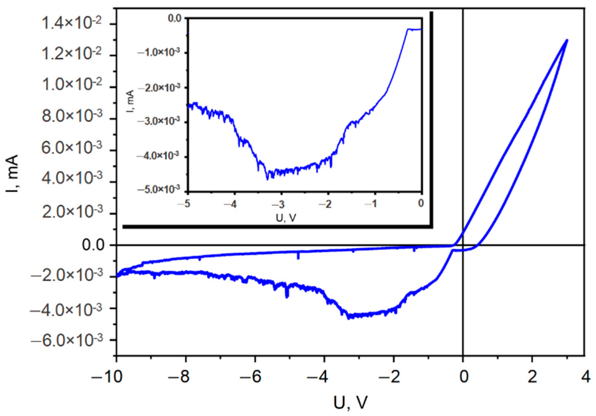
Cyclic voltammetry (CV) measured with a scan rate of 10 mV⋅s−1 was used to study the electrochemical behavior of GaAs substrate in electrolyte containing nickel and iron salts. From CV curve (Figure 1) it can be clearly seen that processes of nickel and iron deposition take part in the potential region up to −3.3 V. At the same time, the hydrogen evolution reaction does not occur in the system, at least up to −10 V, since GaAs substrate is characterized by a moderate resistance and a reported low hydrogen evolution reaction activity [34].
The literature data of NiFe deposition disclose that the used substrate influences the electrochemical deposition process. The same electrolyte concentration was used for NiFe deposition into ion track membranes of polyethylene terephthalate, resulting in NiFe nanotubes composed from the overlapping of small nanodots at an applied potential of −1.75 V [33]. For NiFe deposition on Si semiconductor nanowires, a value of deposition cathodic potential from −1.6 V to −2 V was reported, mentioning that at −1.6 V a non-uniform deposition occurs at the ends of nanowires [35]. To note that the length of used Si nanowires was approximatively 25 µm. In our case, to polarize the whole length of the GaAs nanowires (45 µm long), a higher potential was applied. As a result, the deposition potential −4 V was chosen experimentally for uniform deposition on samples containing GaAs nanowires while at lower deposition potential, the electroplating occurs preponderantly at the bottom of nanowires.
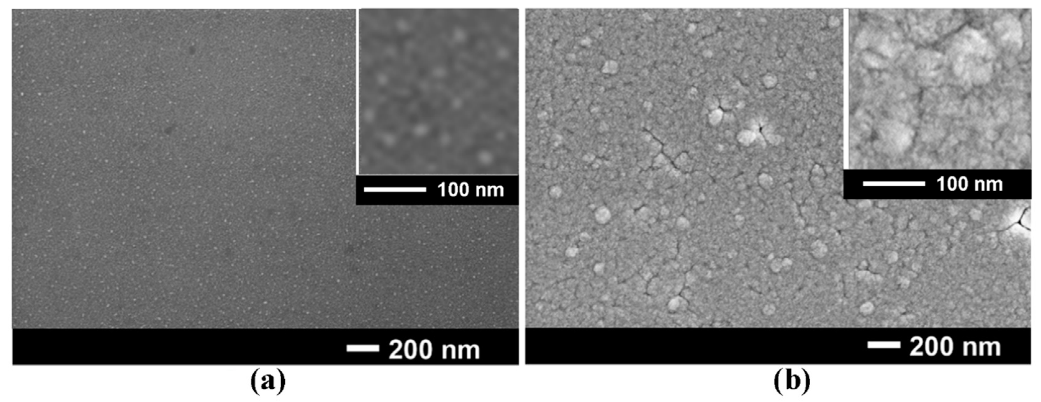
The magnetic properties of coaxial GaAs/NiFe core-shell structures were compared with those of respective alloy coatings on planar GaAs wafers, for the purpose of comparison. The morphology of permalloy coatings on a (111)B GaAs wafer after 40 s and 60 s of potentiostatic deposition are shown in Figure 2.
The coating consists of nanograins with dimensions up to 20 nm after 40 s of deposition, as deduced from the inset in Figure 2a, while the coating after 60 s of deposition represents a nanoporous layer with some randomly distributed grains with dimensions up to (70–80) nm, these having a nanoporous structure (Figure 2b). One should note that the dimensions of nanograins are less than 10 nm after 20 s of deposition, and they do not totally cover the surface of the substrate. On the other hand, conglomerates of nanorods larger than 100 nm occur after 80 s of deposition, which do not ensure a uniform thickness of the shell, and they are not suitable for the purpose of the study.
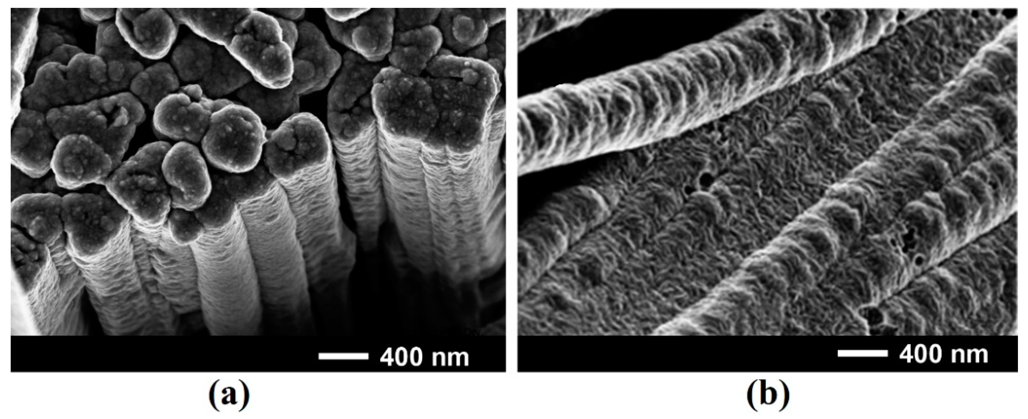
As shown in previous publications, arrays of nanowires with a 200–300 nm diameter and a 45 µm length, oriented preponderantly perpendicularly to the substrate surface preserving the initial (111)B crystallographic orientation of the substrate, are formed as a result of anodization of GaAs wafers in 1M HNO3 electrolyte for 15 min [29]. The morphology of both Ni0.65Fe0.35 and permalloy coatings on such arrays of GaAs nanowires have nanoporous morphology similar to that observed on planar (111)B substrates (see Figure 3).
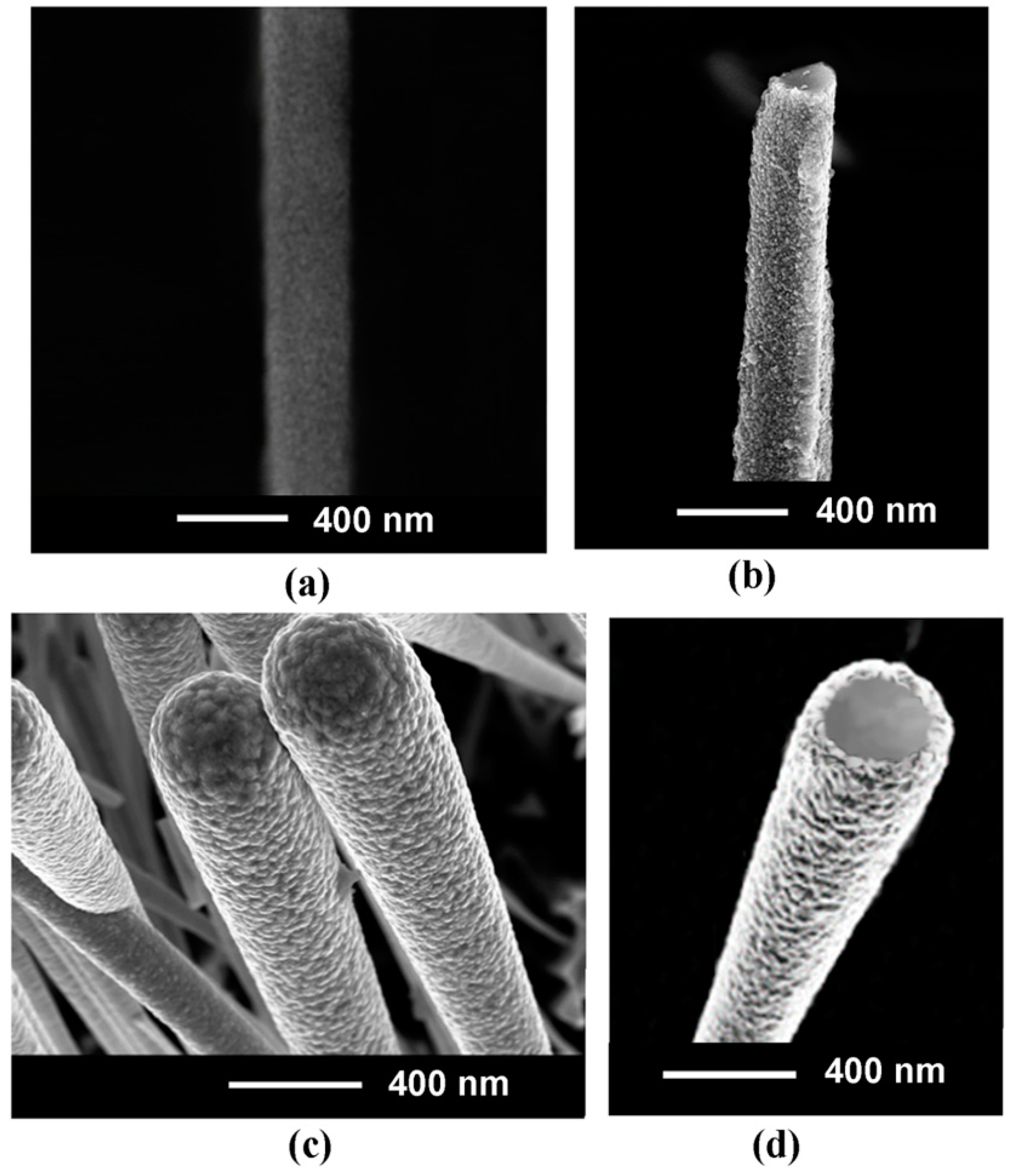
Figure 4 shows the morphology of Ni coatings on GaAs nanowires after deposition for 40 s and 60 s as compared to the image of an initial GaAs nanowire. One can see that the distribution of nanograins is rather uniform over the surface of nanowires, and their size increases with increasing the deposition time, reaching dimensions up to around 50 nm after 60 s deposition. The thickness of the deposited Ni shell can be estimated from images of nanowires cut perpendicularly to their axis after Ni deposition.
The results of EDX analysis of the deposited alloy films summarized in Table 1 show that the compositions of films correspond within the accuracy of ±1% with those set in the electroplating solution. The deviations are determined by the accuracy of the instrument.
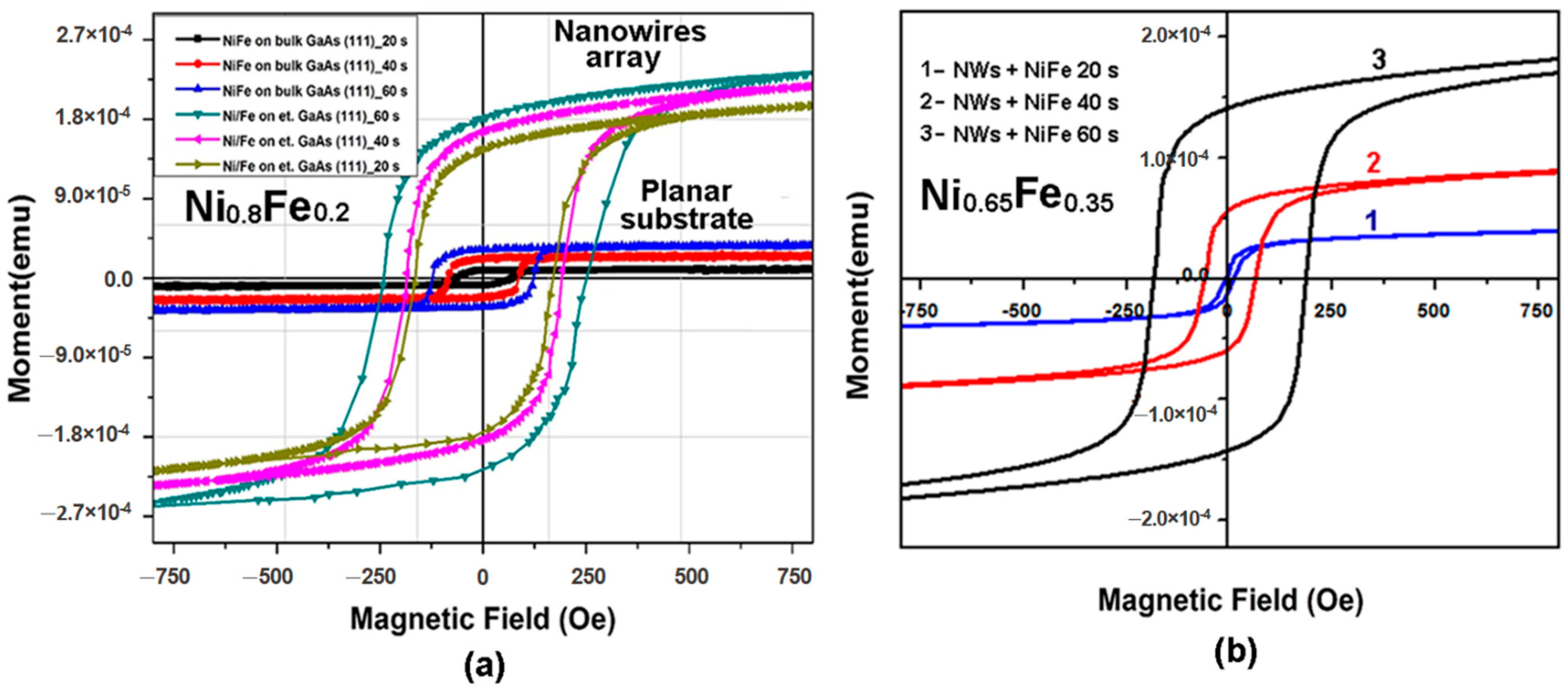
Figure 5a presents hysteresis loops measured on permalloy coatings deposited in potentiostatic mode on GaAs nanowire arrays as compared with those deposited on (111)B GaAs substrates for different periods of time from 20 s to 60 s. One can see that both the magnetic moment and the coercive force are much larger for nanowire arrays than for planar substrates with similar coating thicknesses. The coatings of Ni0.65Fe0.35 alloys on GaAs nanowires (Figure 5b) are more sensitive to the deposition time as compared with permalloy coatings. However, the magnetic parameters have close values for coatings after 60 s deposition.
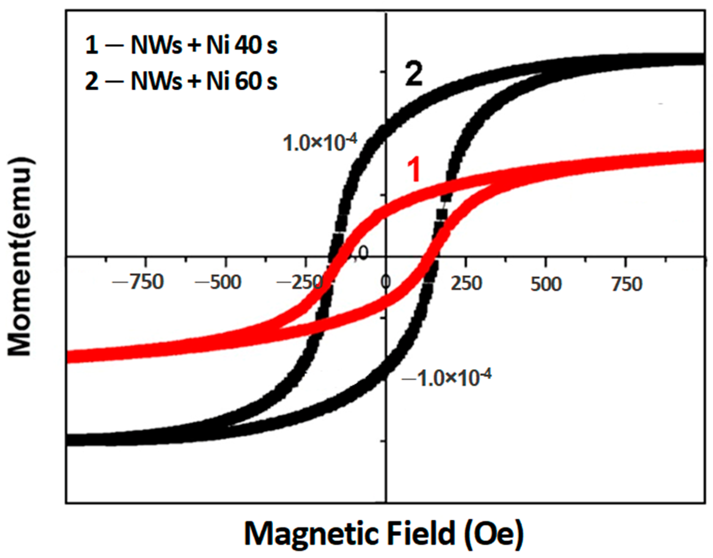
The magnetic parameters (the magnetic moment and the coercive force) of Ni coatings on GaAs nanowire arrays are also not very much different from those of Ni0.65Fe0.35 coatings after the same deposition of 60 s (Figure 6). However, the remanence ratio Mr/Ms (squareness) is lower for the Ni coating as compared to the Ni0.65Fe0.35 and permalloy coatings.
The magnetic characteristics of the investigated samples are summarized in Table 2.
The analysis of data in this table suggests that the coercive force of permalloy coatings on planar substrates is lower than that of Ni0.65Fe0.35 and Ni coatings. At the same time, the coercivity of coaxial core-shell structures is higher than that of planar structures for all the coatings. Apart from that, the coercivity of coaxial permalloy/GaAs core-shell structures is even larger than that of Ni0.65Fe0.35/GaAs and Ni/GaAs structures. The remanence ratio is around 0.67 for both planar and coaxial core-shell structures with Ni0.65Fe0.35 coatings after 60 s deposition. Nearly the same value is observed for coaxial Ni/GaAs core-shell structures, while the remanence ratio is higher (around 0.80) for permalloy/GaAs structures.
A difference in the magnetic parameters of coatings on planar substrates and on nanowires was previously reported for Fe nanoparticle films [30]. This difference was explained in terms of different crystallographic orientations of the substrates and nanowires, which can lead to different coverage with Fe nanoparticles. One needs also to take into account that the geometry of the experiment is different for films deposited on planar substrates from that of films deposited on nanowires.
As concerns nanotube geometries, previous investigations were focused mostly on single crystalline small diameter nanotubes prepared by ALD [13,15,16,17,27]. Their magnetic properties were explained in terms of the magnetic reversal mechanisms related to the movement of different types of domain boundaries: vortex wall and transverse wall [17,27]. On the other hand, the nanotubes forming the shell in core-shell structures prepared in this paper, as well as the Fe shells electroplated in the galvanostatic deposition mode on GaAs nanowires in a previous paper [30], are nanogranular and polycrystalline in their nature. As a result, the observed magnetic behavior of polycrystalline tubular structures is influenced both by the nanograin morphology and the nanotube geometry, and the movement of different types of domain walls is additionally influenced by the nanograin boundaries [30].
4. Conclusions
The results of this study demonstrated that magnetic parameters of GaAs/NiFe structures increase with increasing the NiFe coating thickness. The coercivity of planar GaAs/permalloy structures is lower than that of planar GaAs/NiFe structures with a lower or higher content of Ni, while this does not hold for arrays of coaxial GaAs/NiFe core-shell structures. At the same time, the coercivity of coaxial core-shell structures is larger than that of planar structures. The obtained results pave the way for the exploration of magnetic properties of coaxial core-shell structures for enlarging the area of their applications.
Author Contributions
Conceptualization, E.V.M.; methodology, V.M., M.K.; validation, V.V.U. and K.N.; investigation, V.M., M.K. and E.V.M.; writing—original draft preparation, V.V.U.; writing—review and editing, V.V.U., E.V.M. and I.M.T.; visualization, E.V.M. and V.M.; supervision, I.M.T. and K.N.; project administration, E.V.M. and I.M.T.; funding acquisition, I.M.T. All authors have read and agreed to the published version of the manuscript.
Funding
This research was funded by National Agency for Research and Development of Moldova under the Grants #20.80009.5007.20 and #21.00208.5007.15/PD. The APC was funded by European Commission under the H2020 grant #810652 ‘NanoMedTwin’.
Institutional Review Board Statement
Not applicable.
Informed Consent Statement
Not applicable.
Data Availability Statement
The data presented in this study are available on request from the corresponding authors.
Acknowledgments
E.V.M. acknowledges support from the Alexander von Humboldt Foundation. V.M. acknowledges support from the German Academic Exchange Service for DAAD scholarship at IFW Dresden (Germany).
Conflicts of Interest
The authors declare no conflict of interest. The founding sponsors had no role in the design of the study; in the collection, analyses, or interpretation of data; in the writing of the manuscript, and in the decision to publish the results.
References
- Asare-Yeboah, K.; Li, Q.; Jiang, C.; He, Z.; Bi, S.; Liu, Y.; Liu, C. High Performance and Efficiency Resonant Photo-Effect-Transistor by Near-Field Nano-Strip-Controlled Organic Light Emitting Diode Gate. J. Phys. Chem. Lett. 2020, 11, 6526–6534. [Google Scholar] [CrossRef] [PubMed]
- Li, Q.; Jiang, C.; Bi, S.; Asare-Yeboah, K.; He, Z.; Liu, Y. Photo-Triggered Logic Circuits Assembled on Integrated Illuminants and Resonant Nanowires. ACS Appl. Mater. Interfaces 2020, 12, 46501–46508. [Google Scholar] [CrossRef]
- Bi, S.; Li, Q.; He, Z.; Guo, Q.; Asare-Yeboah, K.; Liu, Y.; Jiang, C. Highly enhanced performance of integrated piezo photo-transistor with dual inverted OLED gate and nanowire array channel. Nano Energy 2019, 66, 104101. [Google Scholar] [CrossRef]
- Mohammed, H.; Moreno, J.A.; Kosel, J. Advanced Fabrication and Characterization of Magnetic Nanowires; IntechOpen: London, UK, 2017; ISBN 978-1-78923-679-8. [Google Scholar]
- Piraux, L. Magnetic Nanowires. Appl. Sci. 2020, 10, 1832. [Google Scholar] [CrossRef]
- Proenca, M.P.; Sousa, C.T.; Ventura, J.; Araújo, J.P. Chapter 6—Cylindrical Magnetic Nanotubes: Synthesis, Magnetism and Applications. In Magnetic Nano- and Microwires, 2nd ed.; Vázquez, M., Ed.; Woodhead Publishing Series in Electronic and Optical Materials; Woodhead Publishing: Thorston, UK, 2020; pp. 135–184. ISBN 978-0-08-102832-2. [Google Scholar]
- García, J.; Manterola, A.M.; Méndez, M.; Fernández-Roldán, J.A.; Vega, V.; González, S.; Prida, V.M. Magnetization Reversal Process and Magnetostatic Interactions in Fe56Co44/SiO2/Fe3O4 Core/Shell Ferromagnetic Nanowires with Non-Magnetic Interlayer. Nanomaterials 2021, 11, 2282. [Google Scholar] [CrossRef]
- Staňo, M.; Fruchart, O. Chapter 3—Magnetic Nanowires and Nanotubes. In Handbook of Magnetic Materials; Brück, E., Ed.; Elsevier: Amsterdam, The Netherlands, 2018; Volume 27, pp. 155–267. [Google Scholar]
- Chong, Y.T.; Görlitz, D.; Martens, S.; Yau, M.Y.E.; Allende, S.; Bachmann, J.; Nielsch, K. Multilayered Core/Shell Nanowires Displaying Two Distinct Magnetic Switching Events. Adv. Mater. 2010, 22, 2435–2439. [Google Scholar] [CrossRef]
- Choudhury, S.; Mondal, S.; De, A.; Barman, A. Chapter 21—Tunable Picosecond Magnetization Dynamics in Ferromagnetic Nanostructures. In 21st Century Nanoscience—A Handbook; Routledge Handbooks Online: London, UK, 2020; p. 488. ISBN 978-0-8153-5626-4. [Google Scholar]
- Chou, S.Y.; Krauss, P.R.; Kong, L. Nanolithographically Defined Magnetic Structures and Quantum Magnetic Disk (Invited). J. Appl. Phys. 1996, 79, 6101–6106. [Google Scholar] [CrossRef]
- Moreno, J.A.; Bran, C.; Vazquez, M.; Kosel, J. Cylindrical Magnetic Nanowires Applications. IEEE Trans. Magn. 2021, 57, 800317. [Google Scholar] [CrossRef]
- Zierold, R.; Nielsch, K. (Invited) Tailor-Made, Magnetic Nanotubes by Template-Directed Atomic Layer Deposition. ECS Trans. 2011, 41, 111. [Google Scholar] [CrossRef]
- Tejo, F.; Vidal-Silva, N.; Espejo, A.P.; Escrig, J. Angular Dependence of the Magnetic Properties of Cylindrical Diameter Modulated Ni80Fe20 Nanowires. J. Appl. Phys. 2014, 115, 17D136. [Google Scholar] [CrossRef]
- Escrig, J.; Daub, M.; Landeros, P.; Nielsch, K.; Altbir, D. Angular Dependence of Coercivity in Magnetic Nanotubes. Nanotechnology 2007, 18, 445706. [Google Scholar] [CrossRef]
- Nielsch, K.; Bachmann, J.; Daub, M.; Jing, J.; Knez, M.; Gösele, U.; Barth, S.; Mathur, S.; Escrig, J.; Altbir, D. Ferromagnetic Nanostructures by Atomic Layer Deposition: From Thin Films Towards Core-Shell Nanotubes. ECS Trans. 2007, 11, 139. [Google Scholar] [CrossRef]
- Daub, M.; Knez, M.; Goesele, U.; Nielsch, K. Ferromagnetic Nanotubes by Atomic Layer Deposition in Anodic Alumina Membranes. J. Appl. Phys. 2007, 101, 09J111. [Google Scholar] [CrossRef]
- Salem, M.S.; Tejo, F.; Zierold, R.; Sergelius, P.; Moreno, J.M.M.; Goerlitz, D.; Nielsch, K.; Escrig, J. Composition and Diameter Modulation of Magnetic Nanowire Arrays Fabricated by a Novel Approach. Nanotechnology 2018, 29, 065602. [Google Scholar] [CrossRef] [PubMed]
- Minguez-Bacho, I.; Rodriguez-López, S.; Vázquez, M.; Hernández-Vélez, M.; Nielsch, K. Electrochemical Synthesis and Magnetic Characterization of Periodically Modulated Co Nanowires. Nanotechnology 2014, 25, 145301. [Google Scholar] [CrossRef] [PubMed]
- Bochmann, S.; Döhler, D.; Trapp, B.; Staňo, M.; Fruchart, O.; Bachmann, J. Preparation and Physical Properties of Soft Magnetic Nickel-Cobalt Three-Segmented Nanowires. J. Appl. Phys. 2018, 124, 163907. [Google Scholar] [CrossRef]
- García, J.; Vega, V.; Iglesias, L.; Prida, V.M.; Hernando, B.; Barriga-Castro, E.D.; Mendoza-Reséndez, R.; Luna, C.; Görlitz, D.; Nielsch, K. Template-Assisted Co–Ni Alloys and Multisegmented Nanowires with Tuned Magnetic Anisotropy. Phys. Status Solidi A 2014, 211, 1041–1047. [Google Scholar] [CrossRef]
- Vega, V.; Böhnert, T.; Martens, S.; Waleczek, M.; Montero-Moreno, J.M.; Görlitz, D.; Prida, V.M.; Nielsch, K. Tuning the Magnetic Anisotropy of Co–Ni Nanowires: Comparison between Single Nanowires and Nanowire Arrays in Hard-Anodic Aluminum Oxide Membranes. Nanotechnology 2012, 23, 465709. [Google Scholar] [CrossRef]
- Pirota, K.R.; Navas, D.; Hernández-Vélez, M.; Nielsch, K.; Vázquez, M. Novel Magnetic Materials Prepared by Electrodeposition Techniques: Arrays of Nanowires and Multi-Layered Microwires. J. Alloys Compd. 2004, 369, 18–26. [Google Scholar] [CrossRef]
- Rumpf, K.; Granitzer, P.; Poelt, P.; Michor, H. (Invited) Pore Filling of Porous Silicon with Ferromagnetic Nanostructures. ECS Trans. 2015, 69, 71. [Google Scholar] [CrossRef]
- Salem, M.S.; Nielsch, K. Crossover between Axial and Radial Magnetic Anisotropy in Self-Organized Permalloy Nanowires. Mater. Sci. Eng. B 2017, 223, 120–124. [Google Scholar] [CrossRef]
- Sorop, T.G.; Nielsch, K.; Göring, P.; Kröll, M.; Blau, W.; Wehrspohn, R.B.; Gösele, U.; de Jongh, L.J. Study of the Magnetic Hysteresis in Arrays of Ferromagnetic Fe Nanowires as a Function of the Template Filling Fraction. J. Magn. Magn. Mater. 2004, 272–276, 1656–1657. [Google Scholar] [CrossRef]
- Albrecht, O.; Zierold, R.; Allende, S.; Escrig, J.; Patzig, C.; Rauschenbach, B.; Nielsch, K.; Görlitz, D. Experimental Evidence for an Angular Dependent Transition of Magnetization Reversal Modes in Magnetic Nanotubes. J. Appl. Phys. 2011, 109, 093910. [Google Scholar] [CrossRef]
- Albrecht, O.; Zierold, R.; Patzig, C.; Bachmann, J.; Sturm, C.; Rheinländer, B.; Grundmann, M.; Görlitz, D.; Rauschenbach, B.; Nielsch, K. Tubular Magnetic Nanostructures Based on Glancing Angle Deposited Templates and Atomic Layer Deposition. Phys. Status Solidi B 2010, 247, 1365–1371. [Google Scholar] [CrossRef]
- Monaico, E.I.; Monaico, E.V.; Ursaki, V.V.; Honnali, S.; Postolache, V.; Leistner, K.; Nielsch, K.; Tiginyanu, I.M. Electrochemical Nanostructuring of (111) Oriented GaAs Crystals: From Porous Structures to Nanowires. Beilstein J. Nanotechnol. 2020, 11, 966–975. [Google Scholar] [CrossRef]
- Monaico, E.V.; Morari, V.; Ursaki, V.V.; Nielsch, K.; Tiginyanu, I.M. Core–Shell GaAs-Fe Nanowire Arrays: Fabrication Using Electrochemical Etching and Deposition and Study of Their Magnetic Properties. Nanomaterials 2022, 12, 1506. [Google Scholar] [CrossRef]
- Leistner, K.; Yang, M.; Damm, C.; Oswald, S.; Petr, A.; Kataev, V.; Nielsch, K.; Kavanagh, K.L. Aligned Cuboid Iron Nanoparticles by Epitaxial Electrodeposition. Nanoscale 2017, 9, 5315–5322. [Google Scholar] [CrossRef]
- Leistner, K.; Duschek, K.; Zehner, J.; Yang, M.; Petr, A.; Nielsch, K.; Kavanagh, K.L. Role of Hydrogen Evolution during Epitaxial Electrodeposition of Fe on GaAs. J. Electrochem. Soc. 2017, 165, H3076. [Google Scholar] [CrossRef]
- Kozlovskiy, A.L.; Korolkov, I.V.; Ibragimova, M.A.; Zdorovets, M.V.; Kutuzau, M.D.; Nikolaevich, L.N.; Shumskaya, E.E.; Kaniukov, E.Y. Magnetic Nanostructured System for Biomedical Applications Based on FeNi Nanotubes. Nanotechnol. Russ. 2018, 13, 331–336. [Google Scholar] [CrossRef]
- Uosaki, K.; Kita, H. Effect of the Ru+++ treatment on the electrochemical hydrogen evolution reaction at GaAs electrodes. Chem. Lett. 1984, 13, 953–956. [Google Scholar] [CrossRef]
- Lamrani, S.; Guittoum, A.; Schäfer, R.; Hemmous, M.; Neu, V.; Pofahl, S.; Hadjersi, T.; Benbrahim, N. Morphology, Structure and Magnetic Study of Permalloy Films Electroplated on Silicon Nanowires. J. Magn. Magn. Mater. 2015, 396, 263–267. [Google Scholar] [CrossRef]
Figure 1.
The cyclic voltammetry scan for a GaAs substrate in NiFe electrolyte. The CV scan of cathodic potential up to −5 V is presented in the inset.
Figure 1.
The cyclic voltammetry scan for a GaAs substrate in NiFe electrolyte. The CV scan of cathodic potential up to −5 V is presented in the inset.

Figure 2.
SEM images of permalloy films on GaAs substrate after 40 s (a) and 60 s (b) deposition.

Figure 3.
SEM images of Ni0.65Fe0.35 (a) and permalloy (b) coatings on GaAs nanowires after deposition for 60 s.
Figure 3.
SEM images of Ni0.65Fe0.35 (a) and permalloy (b) coatings on GaAs nanowires after deposition for 60 s.

Figure 4.
SEM images of an initial GaAs nanowire (a); a GaAs nanowire after Ni coating for 40 s and cutting in a plane perpendicular to the nanowire axis (b); a bunch of GaAs nanowires after Ni coating for 60 s (c); and a GaAs nanowire after Ni coating for 60 s and cutting perpendicularly to the nanowire axis (d).

Figure 5.
Hysteresis loops measured on permalloy-coated bulk (planar) and etched (nanowires) GaAs substrates (a) and Ni0.65Fe0.35-coated GaAs nanowire arrays (b).
Figure 5.
Hysteresis loops measured on permalloy-coated bulk (planar) and etched (nanowires) GaAs substrates (a) and Ni0.65Fe0.35-coated GaAs nanowire arrays (b).

Figure 6.
Hysteresis loops measured on GaAs/Ni core-shell arrays after Ni deposition for 40 s (curve 1) and 60 s (curve 2).
Figure 6.
Hysteresis loops measured on GaAs/Ni core-shell arrays after Ni deposition for 40 s (curve 1) and 60 s (curve 2).


Table 1.
Elemental composition of NiFe alloy films electroplated by potentiostatic deposition.
| Alloy | Element | Weight % | Atomic % |
|---|---|---|---|
| Permalloy | Ni | 82 | 81 |
| Fe | 18 | 19 | |
| Ni0.65Fe0.35 | Ni | 66 | 65 |
| Fe | 34 | 35 | |
| Ni | Ni | 100 | 100 |
Table 2.
Saturation moment, remanence, and coercive forces for electrochemically deposited NiFe and Ni coatings on planar substrates and GaAs nanowires samples for VSM measurements.
Table 2.
Saturation moment, remanence, and coercive forces for electrochemically deposited NiFe and Ni coatings on planar substrates and GaAs nanowires samples for VSM measurements.
| Sample Description | Deposition Mode | Saturation Moment, Ms (emu) × 10−4 | Remanence, Mr (emu) × 10−4 | Coercive Force, Hc (Oe) |
|---|---|---|---|---|
| Planar/Ni0.65Fe0.35 | Potentiost. 20 s | 2.01 | 1.28 | 107 |
| Planar/Ni0.65Fe0.35 | Potentiost. 40 s | 2.27 | 1.46 | 126 |
| Planar/Ni0.65Fe0.35 | Potentiost. 60 s | 2.61 | 1.75 | 153 |
| Nanowires/Ni0.65Fe0.35 | Potentiost. 20 s | 0.37 | 0.11 | 16 |
| Nanowires/Ni0.65Fe0.35 | Potentiost. 40 s | 1.11 | 0.69 | 84 |
| Nanowires/Ni0.65Fe0.35 | Potentiost. 60 s | 1.94 | 1.34 | 172 |
| Planar/Ni0.8Fe0.2 | Potentiost. 20 s | 0.10 | 0.09 | 72 |
| Planar/Ni0.8Fe0.2 | Potentiost. 40 s | 0.25 | 0.22 | 85 |
| Planar/Ni0.8Fe0.2 | Potentiost. 60 s | 0.36 | 0.32 | 123 |
| Nanowires/Ni0.8Fe0.2 | Potentiost. 20 s | 2.05 | 2.60 | 165 |
| Nanowires/Ni0.8Fe0.2 | Potentiost. 40 s | 2.25 | 1.75 | 188 |
| Nanowires/Ni0.8Fe0.2 | Potentiost. 60 s | 2.45 | 1.98 | 250 |
| Planar/Ni | Potentiost. 60 s | 0.80 | 0.74 | 134 |
| Nanowires/Ni | Potentiost. 60 s | 1.55 | 1.05 | 153 |
Publisher’s Note: MDPI stays neutral with regard to jurisdictional claims in published maps and institutional affiliations. |
© 2022 by the authors. Licensee MDPI, Basel, Switzerland. This article is an open access article distributed under the terms and conditions of the Creative Commons Attribution (CC BY) license (https://creativecommons.org/licenses/by/4.0/).
Share and Cite
MDPI and ACS Style
Monaico, E.V.; Morari, V.; Kutuzau, M.; Ursaki, V.V.; Nielsch, K.; Tiginyanu, I.M. Magnetic Properties of GaAs/NiFe Coaxial Core-Shell Structures. Materials 2022, 15, 6262. https://0-doi-org.brum.beds.ac.uk/10.3390/ma15186262
AMA Style
Monaico EV, Morari V, Kutuzau M, Ursaki VV, Nielsch K, Tiginyanu IM. Magnetic Properties of GaAs/NiFe Coaxial Core-Shell Structures. Materials. 2022; 15(18):6262. https://0-doi-org.brum.beds.ac.uk/10.3390/ma15186262
Chicago/Turabian StyleMonaico, Eduard V., Vadim Morari, Maksim Kutuzau, Veaceslav V. Ursaki, Kornelius Nielsch, and Ion M. Tiginyanu. 2022. "Magnetic Properties of GaAs/NiFe Coaxial Core-Shell Structures" Materials 15, no. 18: 6262. https://0-doi-org.brum.beds.ac.uk/10.3390/ma15186262
Note that from the first issue of 2016, this journal uses article numbers instead of page numbers. See further details here.