2.1. General Considerations
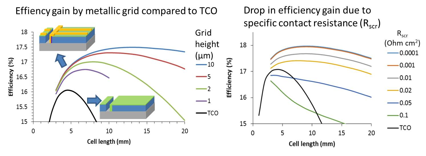
In thin film solar panels, the panel is usually divided into parallel cells that are series connected. There are several ways to accomplish this and
Figure 1 details two of them.
The first is the classic way, in which the TCO is both the front contact and the interconnect (
Figure 1a,b). In this case, the isolation area of the back contact is filled with the semiconducting absorber material and all the current is transported through the TCO. The TCO can be enhanced by a metallic finger grid, while the interconnection between top and bottom electrode takes place at the TCO back contact interface (
Figure 1c,d). Alternatively, a metal busbar can be used for this interconnection purpose (
Figure 1e,f) [
20]. The isolation of the back contact can be filled with a dedicated insulator material [
21]. This approach was mentioned to have more design freedom. In addition, the metal can function both as an interconnection and as a top contact enhancer (
Figure 1g,h). The contact surface area between the front and the back contact, as indicated by the white dashed box, is not changed by these different layouts. In the case of the metal interconnect, the fingers on the TCO will increase the total contact surface area between the metal and the TCO, which is an important feature, as will be discussed in
Section 2.4.
Figure 1.
Schematic representations (not to scale) of different interconnection and cell layouts with a side view (a,c,e,g) and a top view (b,d,f,h). The top image shows the front contact (in green), the absorber material (in blue) and the back contact (in grey). In addition, the separation and interconnection layout between two adjacent cells is shown. The surface area of the TCO/back contact material interface is indicated by the white dashed box. The flow of current is depicted by the arrows. The second highest image shows the case where the front contact is supplemented by a metal grid (in orange), whereas the right image displays the area covered by the metal (not to scale). The third image shows the case of the metal interconnect, for which two material interfaces are important: the metal back contact area represented by the white dashed box and the metal/TCO contact areas represented by the blue dashed box.
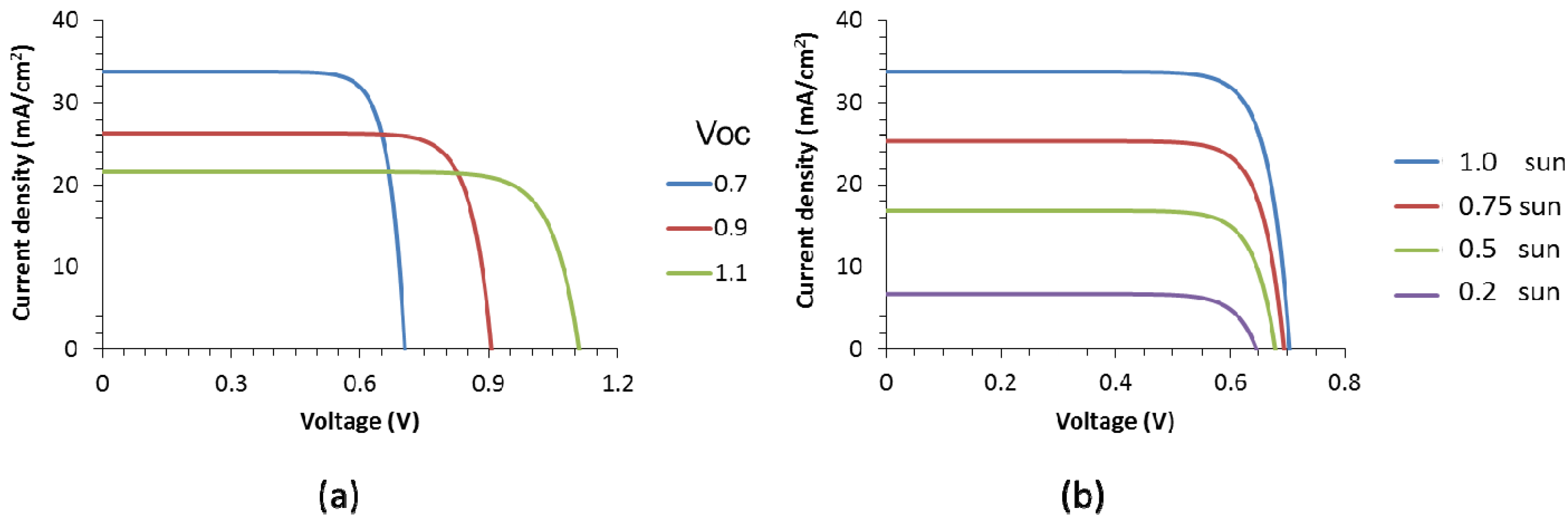
A modest cell efficiency of 19% was chosen, as this has been reported for different thin film materials with various band gaps, which result in different open circuit voltages. Three I-V curves were chosen with an efficiency of 19% and open circuit voltages (Voc) of 0.7, 0.9 and 1.1 V, as to represent typical values for thin film CIGS, CdTe and perovskite solar cells, respectively. The curves are shown in
Figure 2a. More details of the IV curves can be found in the Experimental Section.
Figure 2.
I-V characteristics used for the study (a) cells of 19% efficiency with different open circuit voltages (in V, see legend); and (b) cell with a Voc of 0.7 V for different light intensities (see legend) in which one sun is equivalent to 1000 W/m2).
Figure 2.
I-V characteristics used for the study (a) cells of 19% efficiency with different open circuit voltages (in V, see legend); and (b) cell with a Voc of 0.7 V for different light intensities (see legend) in which one sun is equivalent to 1000 W/m2).
For the curve with a Voc of 0.7 V, the illumination intensity was varied and its effect on the IV curve is shown in
Figure 2b. As the light induced current density goes down, so do the Voc and the fill factor. These curves were used in the modeling to represent reference small cell without interconnection of front contact related losses.
2.2. Cells with a TCO Front Contact
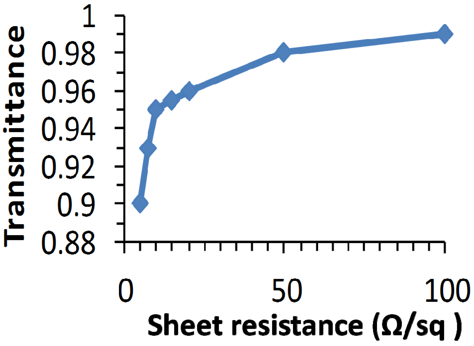
The typical trade-off between transmittance and sheet resistance of the TCO, as used for the modeling, is shown in
Figure 3. Below 10 Ω/sq, the transmittance drops with reduced sheet resistance.
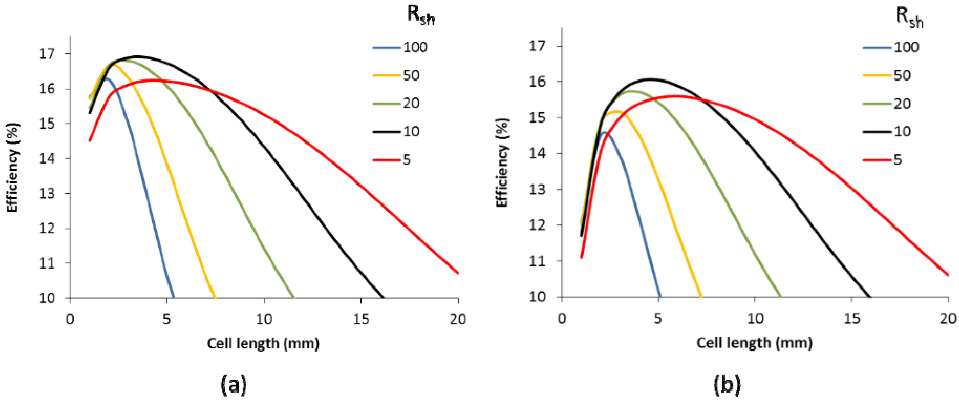
Figure 4a shows the efficiency as a function of the cell length for different TCO sheet resistances. The details of the TCO can be found in the Experimental Section. The cell efficiency shows a maximum with cell length. For very short cells, the optical loss related to the scribing width that is needed for isolation and interconnection is high (here taken to be 150 µm, which is near the lowest reported for CIGS [
22]) compared to the total cell area. For longer cells, the efficiency drops as resistive losses become a major bottleneck. Naturally, a TCO with a lower sheet resistance allows for longer cells. However, as a lower sheet resistance goes together with a lower TCO transmittance [
23,
24], as shown in
Figure 3, there is a trade-off and as is obvious from
Figure 4a, different TCO sheet resistance have a different optimal cell length. A TCO sheet resistance of 5 Ω/sq has a long optimal cell length, but as the transmittance TCO is substantially lower than that of 10 Ω/sq, the efficiency drops from 16.9 % to 16.2%.
Figure 3.
Transmittance as a function of the sheet resistance. This is used to represent TCO induced optical losses in industrially sputtered ZnO: Al material for a wavelength between 400 nm and 1100 nm and do not reflect state of the art laboratory results.
Figure 3.
Transmittance as a function of the sheet resistance. This is used to represent TCO induced optical losses in industrially sputtered ZnO: Al material for a wavelength between 400 nm and 1100 nm and do not reflect state of the art laboratory results.
Figure 4.
Efficiency of solar panels as a function of the individual cell length for different sheet resistances of the TCO (Rsh in Ω/sq) for a scribe width of 150 µm (a) and 350 µm (b). The cell was based on a Voc of 0.7 V.
Figure 4.
Efficiency of solar panels as a function of the individual cell length for different sheet resistances of the TCO (Rsh in Ω/sq) for a scribe width of 150 µm (a) and 350 µm (b). The cell was based on a Voc of 0.7 V.
A maximum efficiency of 16.9% is reached for a TCO sheet resistance of 10 Ω/sq. In other words, when going from a 19% small cell to a solar panel, scribing losses and TCO related losses reduce the panel efficiency by as much as 2 absolute %. When the scribing width is enlarged to 350 µm, which is now a common value in production, the maximum obtainable cell efficiency drops to 16%, as shown in
Figure 4b. This indicates the importance of careful process control and the gain that can be obtained when material removal is more carefully controlled. Moreover, the maximum cell efficiency is obtained at slightly higher cell length, but this difference is rather small. Interestingly, the difference of maximum efficiencies between the high TCOs sheet resistances is increased. This can be explained as follow: a high sheet resistance requires short cells. As the wider scribing width translates to a larger sensitivity to more narrow cells, the impact will be higher.
Figure 5 demonstrates that high band gap materials with higher Voc translate in higher panel efficiencies, even though the small cell efficiency remains 19%. This can be explained by the fact that a higher Voc comes together with a lower short circuit density. This combination brings lower resistive losses. Moreover, lower resistive losses enable longer cells, which help to reduce the optical losses by the scribing width.
Figure 5.
Efficiency of solar panels as a function of the individual cell length for different open circuit voltages (Voc in V) for a scribe width of 150 µm (a) and 350 µm (b). The front contact consists of a TCO of 10 Ω/sq.
Figure 5.
Efficiency of solar panels as a function of the individual cell length for different open circuit voltages (Voc in V) for a scribe width of 150 µm (a) and 350 µm (b). The front contact consists of a TCO of 10 Ω/sq.
If the scribing width is increased to 350 µm, the optimal cell length increases and hence the impact of the Voc on the maximum efficiency, as shown in
Figure 5b. In other words, high Voc cells are less sensitive to scribing width than cells with a low Voc. Therefore, the absorber material not only has an impact on the maximum cell efficiency, but also on the cell layout.
2.3. Cells with Metallic Grid
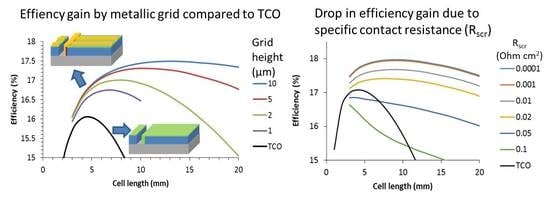
For cells with a metallic grid on top of the TCO, it was found that a TCO of 50 Ω/sq is preferable over a large range of finger widths [
16]. Therefore,
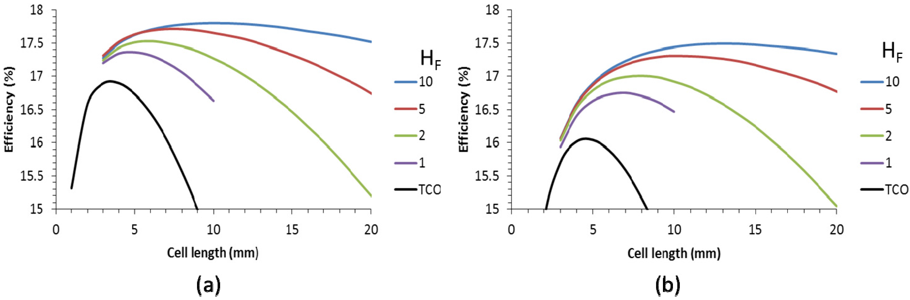
Figure 6 shows the efficiency as a function of the cell length for cells with a 50 Ω/sq TCO supplied with a metallic finger grid with various finger heights (
HF). We also show the values for cells with a 10 Ohm/sq TCO front contact (black line).
For a scribing with of 150 µm (see
Figure 6a), the efficiency increases from just below 17% to 17.8% when a high finger grid is used. For lower finger grid, the efficiency is somewhat lower and the cell length is also smaller. Nevertheless, even for a finger height of 1 µm, the increase in efficiency is 0.5 absolute %. This gain increases when a wider scribing area of 350 µm is taken into account. This is logical, because a TCO only approach cannot accommodate as long cells as compared to TCO supplemented with a finger grid, which show optimal cell lengths that are about twice that of the TCO only configuration. Therefore, the scribe area forms a lower proportion of the total area for longer cells and scribe related losses are proportionally reduced.
Figure 6.
Efficiency of solar panels as function of the individual cell length for TCO-plus-grid front contact with different finger heights (HF, in µm) for a scribe width of 150 µm (a) and 350 µm (b). The cell was based on a Voc of 0.7 V and the finger width is 20 µm. The TCO in the legend refers to calculations with a cell with a TCO of 10 Ω/sq.
A grid finger height of 10 µm could be hard to accomplish for printed lines and the data also indicate the impact of lower finger heights on the cell efficiency and the optimal cell length. On the other hand, the conductivity of the finger material used for this calculation is only 1/5 of the bulk conductivity of copper. Hence, finger material improvement can further increase the efficiency [
25].
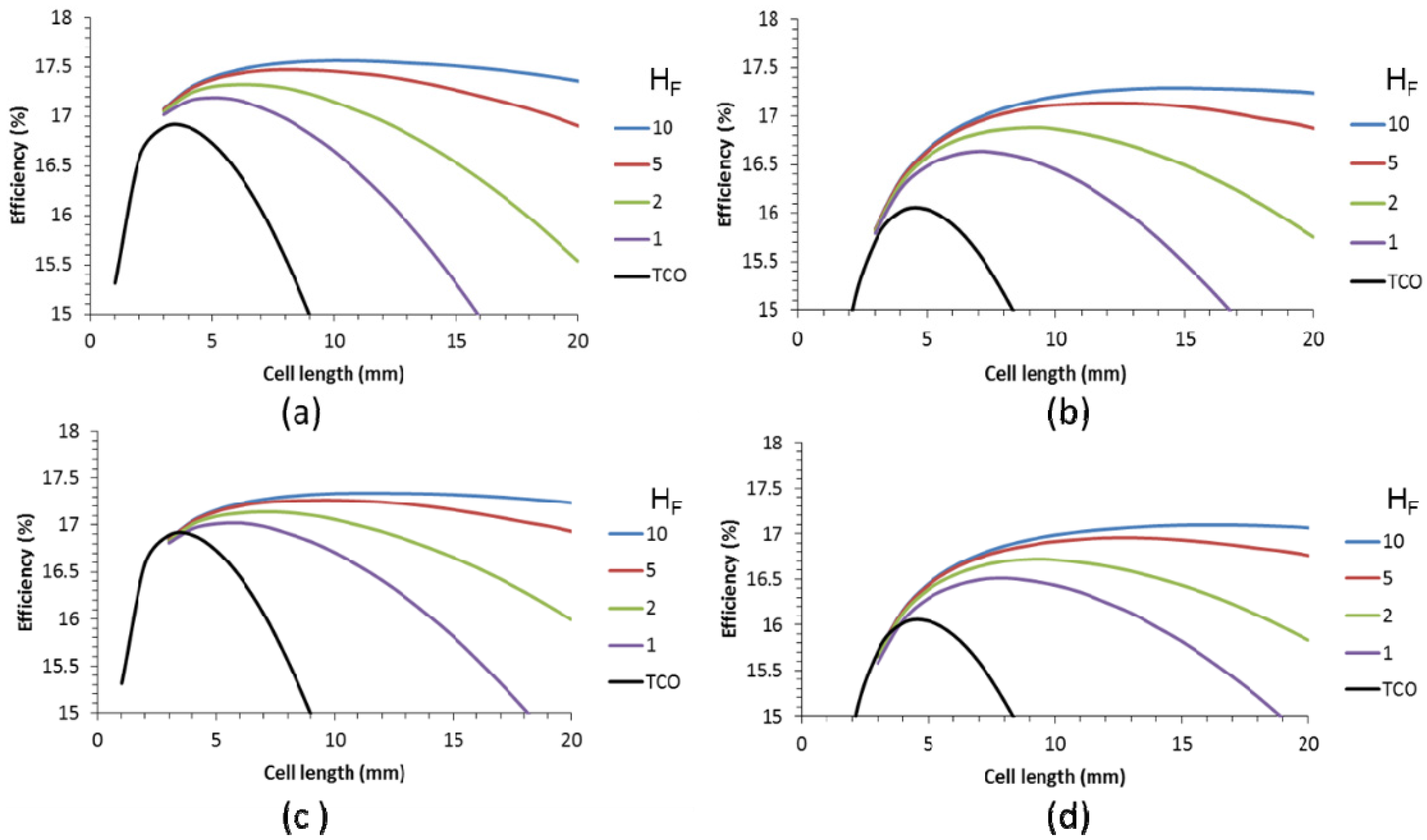
At present, a finger width of 20 µm is not compatible with large area printing technology. For this reason, wider fingers were also used for the calculations to assess the impact of finger width.
Figure 7 shows the efficiency for cell lengths up to 20 mm, various finger heights for two different finger widths of 60 µm (
Figure 7a,b) and 100 µm (
Figure 7c,d). A comparison between a scribing width of 150 µm (
Figure 7a,c) and 350 µm (
Figure 7b,d) are also displayed.
Figure 7.
Efficiency of solar panels as a function of the individual cell length for different grid finger heights (HF, in µm) for a scribe width of 150 µm (a,c) and 350 µm (b,d). The finger width is 60 µm (a,b) and 100 µm (c,d). The data are based on a Voc of 0.7 V.
Figure 7.
Efficiency of solar panels as a function of the individual cell length for different grid finger heights (HF, in µm) for a scribe width of 150 µm (a,c) and 350 µm (b,d). The finger width is 60 µm (a,b) and 100 µm (c,d). The data are based on a Voc of 0.7 V.
Using a wider finger width than 20 µm decreases the efficiency benefit over the TCO only case. Nevertheless, for the presently available scribing width of 350 µm, the impact is still considerable and worth the additional manufacturing step. However, reducing the scribe width to 150 µm reduces the benefit of metallic grids.
2.4. Effect of Contact Resistance
One of the topics in thin film solar cells is the effect of contact resistance, although it is seldom mentioned [
26,
27]. The Mo/CIGS specific contact resistance was reported to be in the order of 0.08 Ohm cm
2 [
28]. However, the specific contact resistance between TCO and Mo was found to be three orders of magnitude lower, in the range of 10
−5 Ω cm
2 [
29]. From the specific contact resistance (R
SCR), the contribution of the contact resistance to the overall resistance in the cell can be estimated. We calculated the contact resistance for a 1 cm
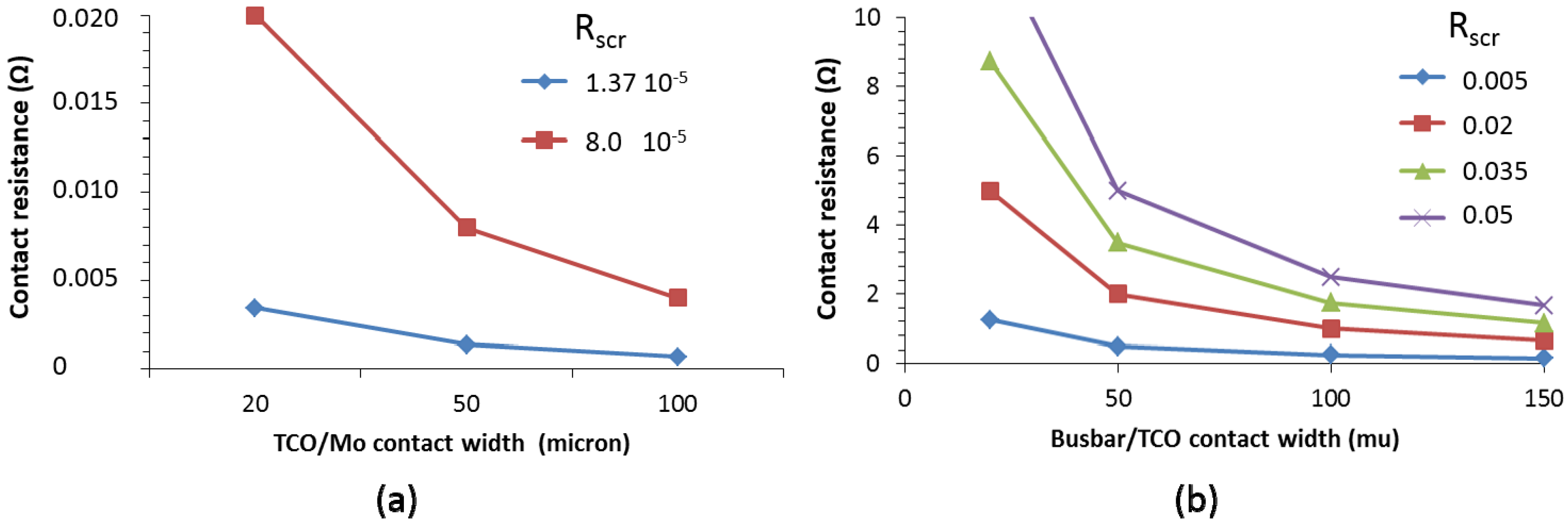
2 cell. This was done for different widths of overlap between the TCO and the Mo, as shown in the TCO/Mo contact width in
Figure 8a. For a 1 cm
2 solar cell, typical total series resistances are between 1 and 2 ohm. For two specific contact resistances (R
scr), the contact resistance was calculated to be less than 0.02 Ω. As this is much lower than the typical series resistance in the cell, the impact is negligible.
Figure 8.
Contact resistance for a 1 cm2 cell as a function of the width of the contact area between the TCO and the Mo (a) and the metal busbar and the TCO (b). The legend shows the specific contact resistance (Rscr, in Ω cm2). The cell length is 5 mm.
Figure 8.
Contact resistance for a 1 cm2 cell as a function of the width of the contact area between the TCO and the Mo (a) and the metal busbar and the TCO (b). The legend shows the specific contact resistance (Rscr, in Ω cm2). The cell length is 5 mm.
For printed lines, the specific contact resistance between the metal and the TCO is between 0.01 and 0.05 Ω cm
2. At present, the factors underlying the contact resistance is under research in our group and include the ink material, the ink curing conditions and the TCO sheet resistance. The contribution of the contact resistance was calculated for a variety of various busbar/TCO overlap (contact) widths and specific contact resistances. Clearly,
Figure 8b shows that the contact resistance is much higher than for the TCO/Mo case and can give a significant contribution to the overall series resistance.
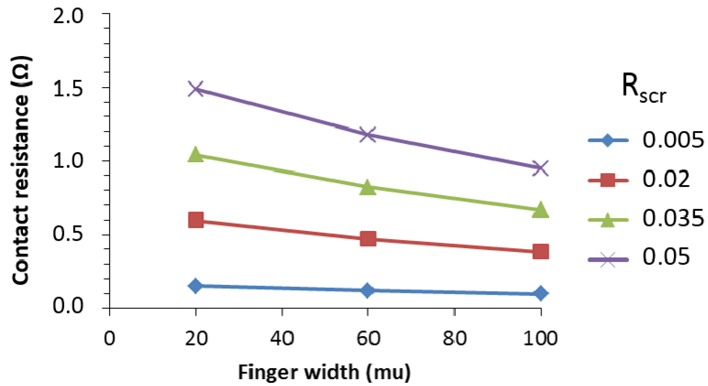
For the case of the metallic interconnect combined with the metallic finger grid, the contact resistance was also calculated. In this case, the busbar width was taken to be 50 µm and the finger widths of 20, 60 and 100 µm were used with a finger spacing is 0.7, 1.6 and 2.1 mm, respectively. As a result of the higher contact area between the metal and the TCO, the contact resistance drops to values below 1.5 Ohm, as shown in
Figure 9. This makes the system more robust against the occurrence of contact resistance between the printed metal and the TCO, although it is not negligible.
Figure 9.
Contact resistance for a cell of 1 cm2 for a cell with metal interconnect and fingers as a function of the finger width for various specific contact resistances (Rscr, in Ω cm2). Ω 2.5. Impact of Contact Resistance on Cell Performance.
Figure 9.
Contact resistance for a cell of 1 cm2 for a cell with metal interconnect and fingers as a function of the finger width for various specific contact resistances (Rscr, in Ω cm2). Ω 2.5. Impact of Contact Resistance on Cell Performance.
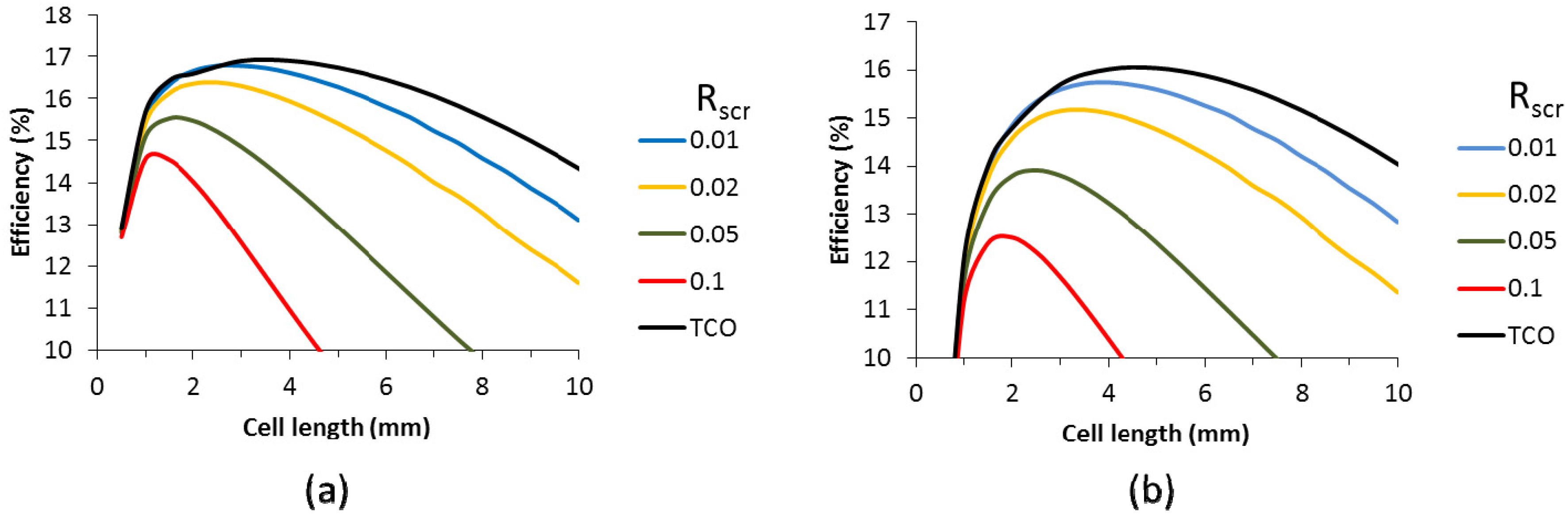
The effect of the contact resistance on the cell performance was calculated for the case without and with metallic grid. For the case without metallic grid, the data are presented in
Figure 10 for a scribe with of 150 µm and 350 µm. We have used the range of specific contact resistance between 0.01 and 0.1 Ω cm
2. The black lines indicate the case without contact resistance (TCO interconnect). A specific contact resistance of 0.01 Ω cm
2 has only minimal impact on the cell efficiency. However, for higher specific contact resistances, the impact is larger and the efficiency drops several absolute percent for the highest specific contact resistances calculated. For a scribe width of 350 µm, the drop in efficiency is even more dramatic. This is caused by the fact that the wider scribing width induces a higher optimal cell length. The longer cells generate more current and translate into a larger effect of the series resistance. In this respect, the occurrence of contact resistance is an extra motivation to minimize the scribe width.
Figure 10.
Efficiency as a function of the cell length and specific contact resistance for cells with 150 µm (a) and 350 µm (b) scribe width.
Figure 10.
Efficiency as a function of the cell length and specific contact resistance for cells with 150 µm (a) and 350 µm (b) scribe width.
For cells with a 50 Ω/sq TCO supplemented with a metallic finger grid, the impact of the specific contact resistance was calculated for finger widths of 20 µm and 60 µm and various finger heights, as shown in
Figure 11. A scribing width of 150 µm was used. We have included lower specific contact resistances to demonstrate that extremely low values do not impact the cell efficiency. However, from a specific contact resistance of 0.01 and upward, a consistent decrease in cell efficiency and optimal cell length is seen. Above a R
scr of 0.02, the efficiency enhancement by the metallic grid compared to the TCO is only very small. Higher finger grids can compensate for this to some extent, but nevertheless,
Figure 11 indicates that for a competitive performance of finger grids and metallic interconnect over the classic TCO interconnect, the R
scr should be at least 0.02 Ω cm
2.
Figure 11.
Efficiency as a function of the cell length for various specific contact resistances (see legend, Rscr, in Ω cm2), and TCO (without contact resistance) for cells with finger grid width of 20 µm (a,c,e) and 60 µm (b,d,f) and a height of 2 µm (a,b), 5 µm (c,d) and 50 µm (e,f). Calculations were based on a 19% small cell.
The effect of the Rscr is smaller for wider grids. This can be explained by the larger contact area between the metal and the finger. As a result, for an Rscr of 0.02 Ohm cm2 there is little difference in efficiency between the 20 µm and the 60 µm grid widths. The benefit of the lower shadow of the narrower grid finger is compensated by the higher contact resistance loss. This is independent of the grid height. Obviously, for higher grid fingers, the range of the applicable cell length increases, but the impact of the Rscr is similar. A longer cell increases both the contact area and the generated current and these two factors counterbalance each other.
In contrast,
Figure 10 shows an increased impact of R
scr with cell length, as in this case, the longer cell length increases the current density, but the TCO metal contact area (busbar only) remains the same. For all cells with a metallic interconnect, the cells with a metallic grid show a higher cell efficiency (
Figure 11) compared to the cells with only a TCO as the front contact for similar R
scr (
Figure 10).
2.6. Influence of Illumination Power
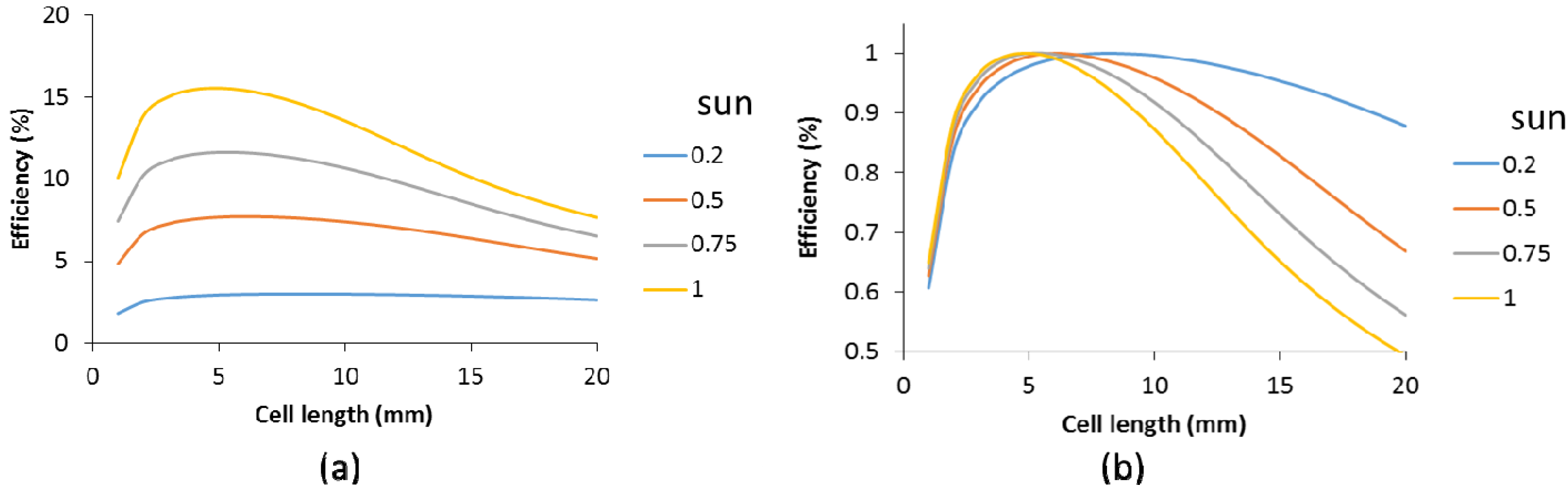
Solar panels and solar cells are tested and certified at an illumination power of 1000 W/m
2 (also denoted as one sun). Therefore, the panel configuration is usually optimized for this high intensity. However, in northwest Europe, this high power is seldom reached. In real life, much of the power generated by solar panels is actually around an illumination power of 500 W/m
2. For cells without a metallic grid, the influence of the illumination power was investigated with variation of the cell length, as shown in
Figure 12a. Seemingly, as the illumination power decreases, the impact of the cell length drops. However, when these data are normalized, as shown in
Figure 12b, it is seen that the relative power is merely shifted toward somewhat higher cell lengths and the impact is reduced for longer cells. Nevertheless, down to an illumination power of 0.5 suns, the cell length remains a critical part of the configuration optimization.
Figure 12.
Efficiency as function of the cell length for different light intensities (see legend in sun units, whereby one sun is 1000 W/m2): (a) calculated values; (b) normalized values.
Figure 12.
Efficiency as function of the cell length for different light intensities (see legend in sun units, whereby one sun is 1000 W/m2): (a) calculated values; (b) normalized values.
For cells with a finger grid, the cell efficiency seems to become less affected by the cell length, as shown in
Figure 13, which shows efficiency as function of the cell length for illumination powers from 0.2 to 1 sun in
Figure 13a–d. Note that for each graph, the minimum value on the x-axis is about half of the maximum value to facilitate comparison with
Figure 12b.
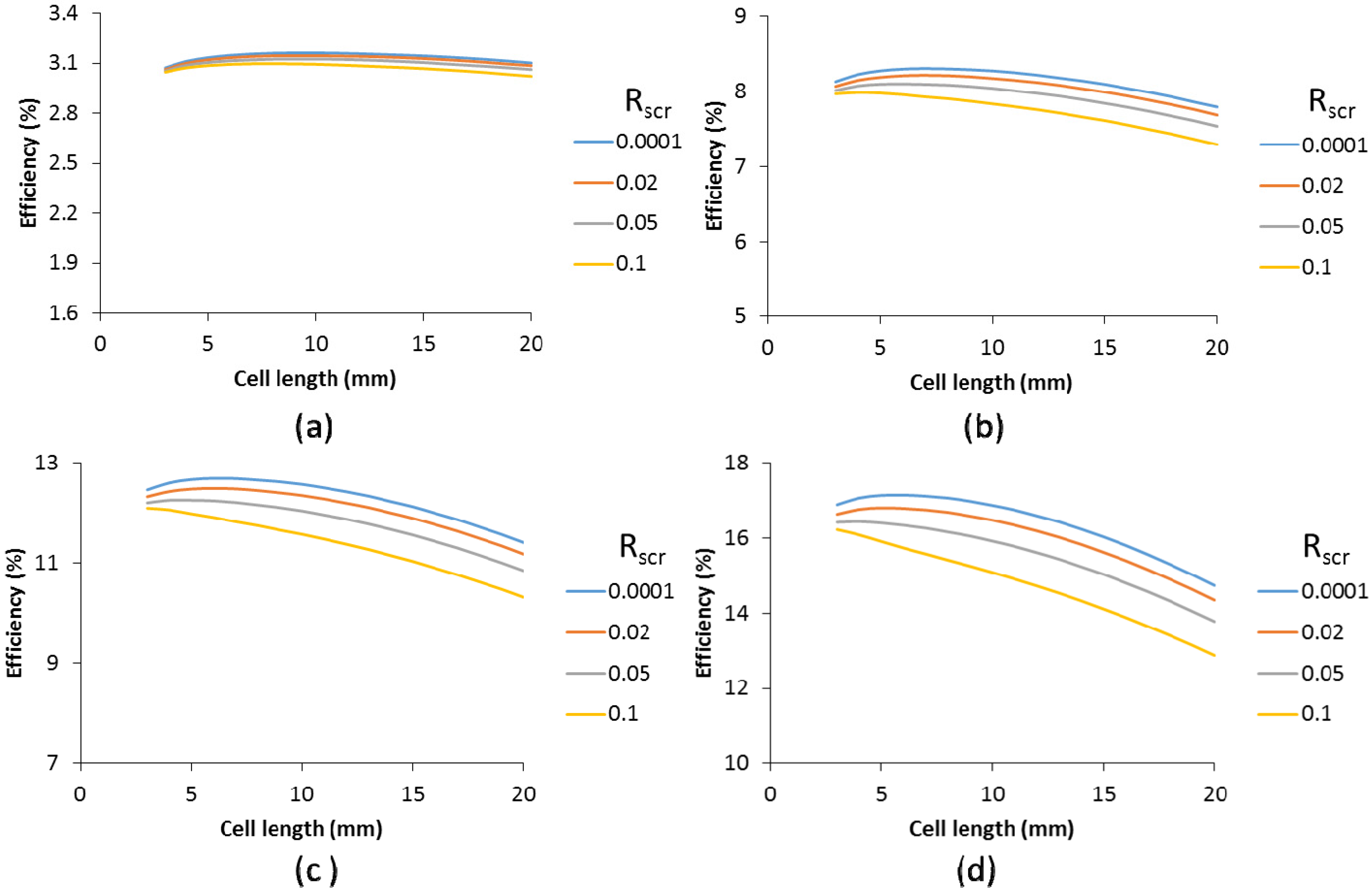
Figure 13.
Efficiency as function of the cell length for various specific contact resistances (Rscr, in Ohm cm2) for light intensity of: 0.2 sun (a); 0.5 sun (b); 0.75 sun (c); and 1 sun (d).
Figure 13.
Efficiency as function of the cell length for various specific contact resistances (Rscr, in Ohm cm2) for light intensity of: 0.2 sun (a); 0.5 sun (b); 0.75 sun (c); and 1 sun (d).
An additional observation is that lower illumination intensity reduces the impact of the specific contact resistance. In other words, the expected impact of the specific contact resistance for cells with metallic grids on the yearly yield of a solar panel is less than posed in
Figure 10, which was based on an illumination power of one sun. Although this suggests that the R
scr is a less severe bottleneck, an R
scr below 0.02 Ω cm
2 is still highly recommended.


