
High Pressure Deuterium Passivation of Charge Trapping Layer for Nonvolatile Memory Applications


Abstract
:1. Introduction
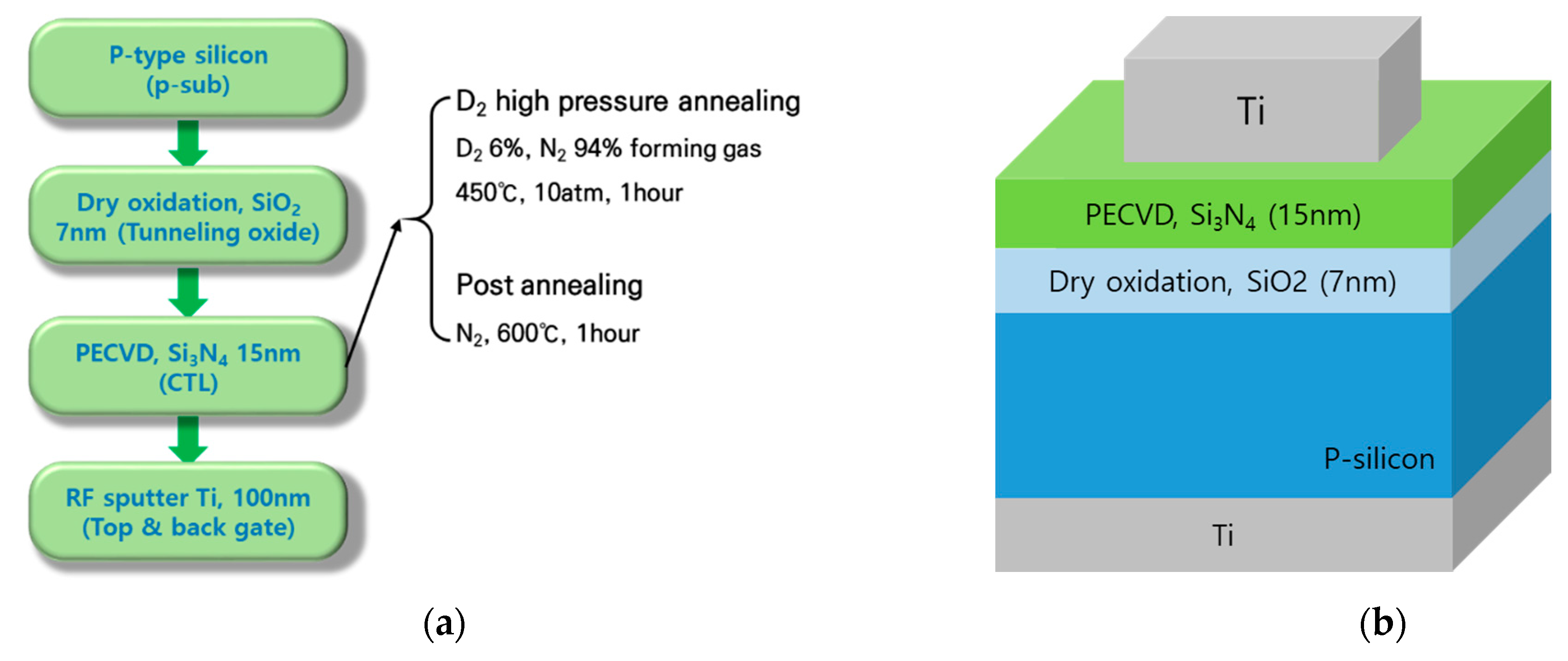
2. Experiments
3. Results and Discussion
3.1. Electrical Analysis
3.1.1. Memory Window
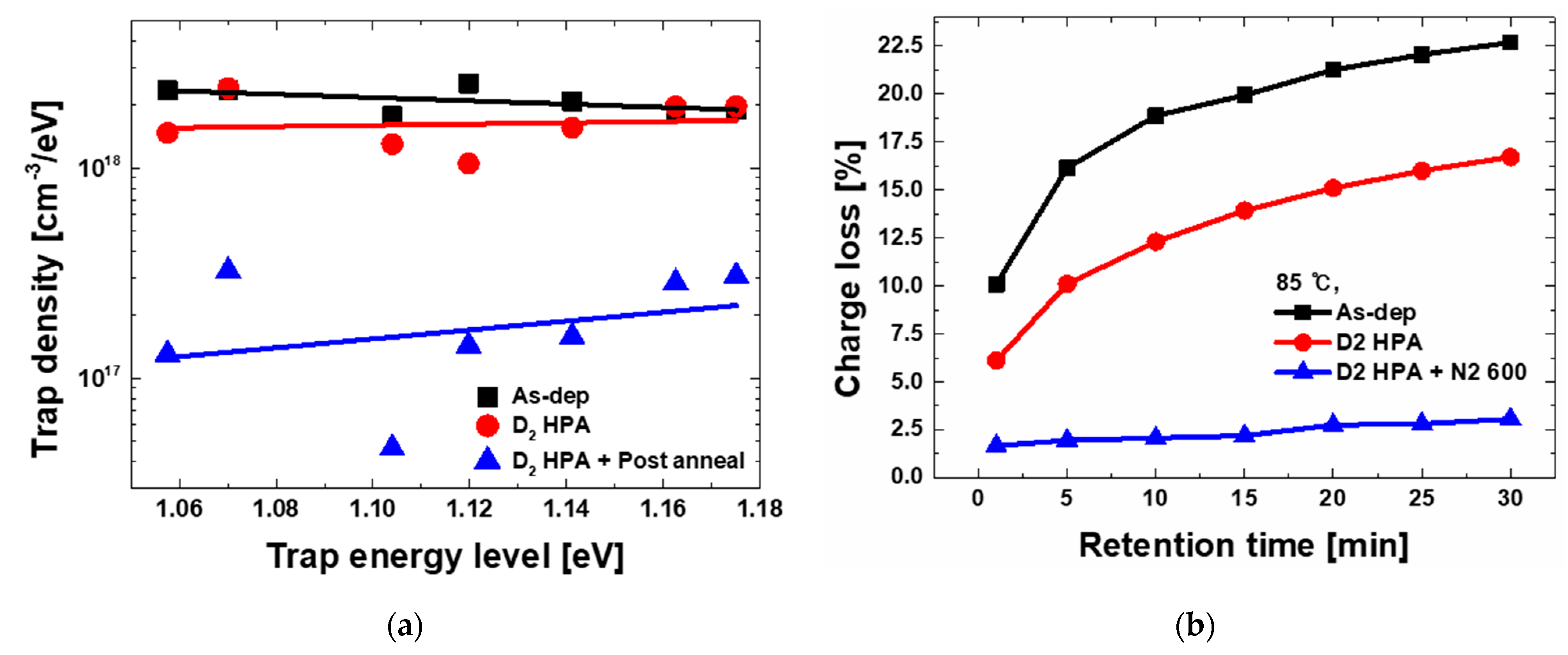
3.1.2. Retention Characteristics
3.1.3. Trap Energy Level Distribution
3.2. Physical Analysis
3.2.1. Secondary Ion Mass Spectroscopy
3.2.2. Fourier Transform InfraRed Spectroscopy
4. Conclusions
Author Contributions
Funding
Conflicts of Interest
References
- Qin, S.; Jiang, Z.; Li, H.; Fujii, S.; Lee, D.; Wong, S.S.; Wong, H.S.P. Next-generation ultrahigh-density 3D vertical resistive switching memory (VRSM)-Part I: Accurate and Computationally Efficient Modeling. IEEE Trans. Electron Devices 2019, 66, 5139–5146. [Google Scholar] [CrossRef]
- Endoh, T.; Honjo, H.; Nishioka, K.; Ikeda, S. Progresses in STT-MRAM and SOT-MRAM for Next Generation MRAM. In Proceedings of the 2020 IEEE Symposium on VLSI Technology, Honolulu, HI, USA, 16–19 June 2020. [Google Scholar]
- Ishimaru, K. Challenges of flash memory for next decade. In Proceedings of the 2021 IEEE International Reliability Physics Symposium (IRPS), Monterey, CA, USA, 23 January 2021. [Google Scholar]
- Chen, T.S.; Wu, K.H.; Chung, H.; Kao, C.H. Performance improvement of SONOS memory by bandgap engineering of charge-trapping layer. IEEE Electron Device Lett. 2004, 25, 205–207. [Google Scholar] [CrossRef]
- Wang, S.Y.; Lue, H.T.; Lai, E.K.; Yang, L.W.; Yang, T.; Chen, K.C.; Gong, J.; Hsieh, K.Y.; Liu, R.; Lu, C.Y. Reliability and processing effects of bandgap engineered SONOS (BESONOS) flash memory. In Proceedings of the 2007 IEEE International Reliability Physics Symposium Proceedings 45th Annual, Phoenix, AZ, USA, 1–19 April 2007. [Google Scholar]
- Kim, H.D.; An, H.M.; Kim, K.C.; Seo, Y.J.; Kim, T.G. Influence of post-annealing on the electrical properties of metal/oxide/silicon nitride/oxide/silicon capacitors for flash memories. Semicond. Sci. Technol. 2008, 23, 075046. [Google Scholar] [CrossRef]
- Lim, J.G.; Yang, S.D.; Yun, H.J.; Jung, J.K.; Park, J.H.; Lim, C.; Cho, G.S.; Park, S.G.; Huh, C.; Lee, H.D.; et al. High performance SONOS flash memory with in-situ silicon nanocrystals embedded in silicon nitride charge trapping layer. Solid-State Electron. 2018, 140, 134–138. [Google Scholar] [CrossRef]
- Furnemont, A.; Zahid, M.B.; Degraeve, R.; Breuil, L.; Cacciato, A.; Rothschild, A.; Olsen, C.; Ganguly, U.; Van Houdt, J. Nitride engineering for improved erase performance and retention of TANOS NAND Flash memory. In Proceedings of the 2008 Joint Non-Volatile Semiconductor Memory Workshop and International Conference on Memory Technology and Design, Opio, France, 18–22 May 2008. [Google Scholar]
- Chasin, A.; Franco, J.; Bury, E.; Ritzenthaler, R.; Litta, E.; Spessot, A.; Horiguchi, N.; Linten, D.; Kaczer, B. Relevance of fin dimensions and high-pressure anneals on hot-carrier degradation. In Proceedings of the 2020 IEEE International Reliability Physics Symposium (IRPS), Dallas, TX, USA, 28 April–30 May 2020. [Google Scholar]
- Park, J.Y.; Yoo, T.J.; Yu, J.M.; Lee, B.H.; Choi, Y.K. Impact of Post-Metal Annealing WITH Deuterium or Nitrogen for Curing a Gate Dielectric Using Joule Heat Driven by Punch-Through Current. IEEE Electron Device Lett. 2020, 42, 276–279. [Google Scholar] [CrossRef]
- Lee, J.; Cheng, K.; Chen, Z.; Hess, K.; Lyding, J.W.; Kim, Y.K.; Lee, H.S.; Kim, Y.W.; Suh, K.P. Application of high pressure deuterium annealing for improving the hot carrier reliability of CMOS transistors. IEEE Electron Device Lett. 2000, 21, 221–223. [Google Scholar]
- Tanaka, M.; Saida, S.; Mitani, Y.; Mizushima, I.; Tsunashima, Y. Highly reliable MONOS Devices with optimized silicon nitride film having deuterium terminated charge traps. In Proceedings of the Digest International Electron Devices Meeting, San Francisco, CA, USA, 8–11 December 2002. [Google Scholar]
- Choi, S.; Baek, S.; Jang, M.; Jeon, S.; Kim, J.; Kim, C.; Hwang, H. Effects of High-Pressure Deuterium annealing on nonvolatile memory device with silicon nanocrystals embedded in silicon nitride. J. Electrochem. Soc. 2005, 152, G345. [Google Scholar] [CrossRef]
- Choi, S.; Jang, M.; Park, H.; Hwang, H.; Jeon, S.; Kim, J.; Kim, C. High-pressure deuterium annealing for improving the reliability characteristics of silicon-oxide-nitride-oxide-silicon nonvolatile memory devices. Appl. Phys. Lett. 2004, 85, 6415–6417. [Google Scholar] [CrossRef]
- Breuil, L.; Lisoni, J.G.; Delhougne, R.; Tan, C.L.; Van Houdt, J.; Furnemont, A. Improvement of poly-Si channel vertical charge trapping NAND devices characteristics by high pressure D2/H2 annealing. In Proceedings of the 2016 IEEE 8th International Memory Workshop (IMW), Paris, France, 15–18 May 2016. [Google Scholar]
- Yu, J.M.; Park, J.Y.; Yoo, T.J.; Han, J.K.; Yun, D.H.; Lee, G.B.; Hur, J.; Lee, B.H.; Kim, S.Y.; Lee, B.H.; et al. Quantitative analysis of high-pressure Deuterium annealing effects on vertically stacked Gate-All-Around SONOS memory. IEEE Trans. Electron. Devices 2020, 67, 3903–3907. [Google Scholar] [CrossRef]
- Schmidt, J.; Schuurmans, F.M.; Sinke, W.C.; Glunz, S.W.; Aberle, A.G. Observation of multiple defect states at silicon-silicon nitride interfaces fabricated by low-frequency plasma enhanced chemical vapor deposition. Appl. Phys. Lett. 1997, 71, 252–254. [Google Scholar] [CrossRef]
- Perera, R.; Ikeda, A.; Hattori, R.; Kuroki, Y. Effects of post annealing on removal of defect states in silicon oxynitride films grown by oxidation of silicon substrates nitride in inductively couple nitrogen plasma. Thin Solid Film. 2003, 423, 212–217. [Google Scholar] [CrossRef]
- Hess, K.; Kizilyalli, I.C.; Lyding, J.W. Giant Isotope Effect in Hot Electron Degradation of Metal Oxide Silicon Devices. IEEE Trans. Electron Devices 1998, 45, 406–416. [Google Scholar] [CrossRef] [Green Version]
- Scardera, G.; Puzzer, T.; Conibeer, G.; Green, M.A. Fourier transform infrared spectroscopy of annealed silicon-rich silicon nitride thin films. J. Appl. Phys. 2008, 104, 104310. [Google Scholar] [CrossRef]
- Lu, Z.; Santos-Filho, P.; Stevens, G.; Williams, M.J.; Lucovsky, G. Fourier transform infrared study of rapid thermal annealing of aSi_N_H(D) films prepared by remote plasma enhanced chemical vapor deposition. J. Vac. Sci. Technol. A Vac. Surf. Film. 1995, 13, 607–613. [Google Scholar] [CrossRef]
- Sandhya, C.; Ganguly, U.; Singh, K.K.; Singh, P.K.; Olsen, C.; Seutter, S.M.; Hung, R.; Conti, G.; Ahmed, K.; Krishna, N.; et al. Nitride Engineering and the effect of interfaces on charge trap flash performance and reliability. In Proceedings of the 2008 IEEE International Reliability Physics Symposium, Phoenix, AZ, USA, 27 April–1 May 2008. [Google Scholar]
- Yang, Y.L.; White, M.H. Charge retention of scaled SONOS nonvolatile memory devices at elevated temperatures. Solid-State Electron. 2000, 44, 949–958. [Google Scholar] [CrossRef]
- Chang, M.; Hasan, M.; Jung, S.; Park, H.; Jo, M.; Choi, H.; Hwang, H. Impact of high-pressure deuterium oxide annealing on the blocking efficiency and interface quality of metal-alumina-nitride-oxide-silicon-type flash memory devices. Appl. Phys. Lett. 2007, 91, 192111. [Google Scholar] [CrossRef]
- Carlson, D.E.; Magee, C.W. A SIMS analysis of deuterium diffusion in hydrogenated amorphous silicon. Appl. Phys. Lett. 1978, 33, 81–83. [Google Scholar] [CrossRef]


| As-Deposited | D2 HPA | D2 HPA + Post Anneal | |
|---|---|---|---|
| D2, 450 °C, 10 atm | × | O | O |
| N2, 600 °C | × | × | O |
| Temperature | 85 °C | 100 °C | 125 °C |
| As-dep | 19.43 | 27.53 | 35.65 |
| D2 HPA | 16.75 | 21.37 | 27.65 |
| D2 HPA + Post-anneal | 10.30 | 10.52 | 9.84 |
Publisher’s Note: MDPI stays neutral with regard to jurisdictional claims in published maps and institutional affiliations. |
© 2021 by the authors. Licensee MDPI, Basel, Switzerland. This article is an open access article distributed under the terms and conditions of the Creative Commons Attribution (CC BY) license (https://creativecommons.org/licenses/by/4.0/).
Share and Cite
Sung, J.-Y.; Jeong, J.-K.; Ko, W.-S.; Byun, J.-H.; Lee, H.-D.; Lee, G.-W. High Pressure Deuterium Passivation of Charge Trapping Layer for Nonvolatile Memory Applications. Micromachines 2021, 12, 1316. https://0-doi-org.brum.beds.ac.uk/10.3390/mi12111316
Sung J-Y, Jeong J-K, Ko W-S, Byun J-H, Lee H-D, Lee G-W. High Pressure Deuterium Passivation of Charge Trapping Layer for Nonvolatile Memory Applications. Micromachines. 2021; 12(11):1316. https://0-doi-org.brum.beds.ac.uk/10.3390/mi12111316
Chicago/Turabian StyleSung, Jae-Young, Jun-Kyo Jeong, Woon-San Ko, Jun-Ho Byun, Hi-Deok Lee, and Ga-Won Lee. 2021. "High Pressure Deuterium Passivation of Charge Trapping Layer for Nonvolatile Memory Applications" Micromachines 12, no. 11: 1316. https://0-doi-org.brum.beds.ac.uk/10.3390/mi12111316