Miniaturized Memory Devices

A special issue of Micromachines (ISSN 2072-666X). This special issue belongs to the section "A:Physics".

Deadline for manuscript submissions: closed (30 September 2022) | Viewed by 7084

Special Issue Editors


E-Mail
Guest Editor
De Montfort University, Leicester, UK
Interests: nanomaterials; thin films; memory; photovoltaics; digital manufacturing

E-Mail Website
Guest Editor
De Montfort University, Leicester, UK
Interests: emerging electronic memory devices; nanomaterials; photovoltaic solar cells; low-temperature manufacturing processes; batteries

Special Issue Information

Dear Colleagues,

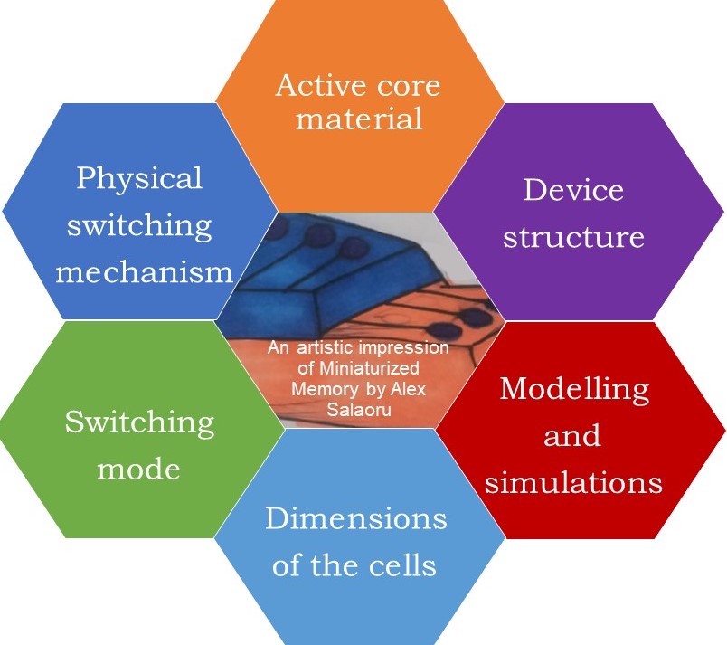
Nowadays, electronic memory elements are an essential component of all electronic devices, from computers to toys and from heath monitors to space technology. Furthermore, the solid-state implementations of these devices show great potential in such applications as artificial synapses, neuromorphic computing, and reconfigurable architectures. Numerous candidates for emerging electronic memory technologies, such as ferroelectric (FeRAM), phase change random access memory (PCRAM), magnetoresistive (MRAM), resistive random access memory (ReRAM), macromolecular, and Mott memory devices, as well as organic memory, etc., have been reported. On the other side, the miniaturization concept was proposed, for first time, by Richard Feynman in his lecture “Plenty of Room at the Bottom”. His theoretical concept has materialized in the electronic devices sector with miniaturization being one of the current trends in electronics.

This Special Issue will encompass a few of the most important aspects that are shared by all types of memories, such as fabrication, investigation of physical switching/charging mechanism(s), mathematical modeling, and applications; these are but a few examples, and the Special Issue is therefore open to additional aspects of fields related to memory. For this Special Issue, we invite contributions from both academia and the industry.

Dr. Iulia Salaoru
Prof. Shashi Paul
Guest Editors

Manuscript Submission Information

Manuscripts should be submitted online at www.mdpi.com by registering and logging in to this website. Once you are registered, click here to go to the submission form. Manuscripts can be submitted until the deadline. All submissions that pass pre-check are peer-reviewed. Accepted papers will be published continuously in the journal (as soon as accepted) and will be listed together on the special issue website. Research articles, review articles as well as short communications are invited. For planned papers, a title and short abstract (about 100 words) can be sent to the Editorial Office for announcement on this website.

Submitted manuscripts should not have been published previously, nor be under consideration for publication elsewhere (except conference proceedings papers). All manuscripts are thoroughly refereed through a single-blind peer-review process. A guide for authors and other relevant information for submission of manuscripts is available on the Instructions for Authors page. Micromachines is an international peer-reviewed open access monthly journal published by MDPI.

Please visit the Instructions for Authors page before submitting a manuscript. The Article Processing Charge (APC) for publication in this open access journal is 2600 CHF (Swiss Francs). Submitted papers should be well formatted and use good English. Authors may use MDPI's English editing service prior to publication or during author revisions.

Keywords

  • Organic/polymer memory (including macromolecular memory)
  • Transition metal oxide memory
  • Carbon-based memory
  • Phase change memory
  • Ferroelectric memory
  • Magnetoresistive
  • Flash memory devices (including nitride traps (SONOS))
  • Mott memory

Published Papers (3 papers)

Order results
Result details
Select all
Export citation of selected articles as:

Research

9 pages, 3463 KiB  
Article
Physical and Electrical Analysis of Poly-Si Channel Effect on SONOS Flash Memory
by Jun-Kyo Jeong, Jae-Young Sung, Woon-San Ko, Ki-Ryung Nam, Hi-Deok Lee and Ga-Won Lee
Micromachines 2021, 12(11), 1401; https://0-doi-org.brum.beds.ac.uk/10.3390/mi12111401 - 15 Nov 2021
Cited by 4 | Viewed by 2509
Abstract
In this study, polycrystalline silicon (poly-Si) is applied to silicon-oxide-nitride-oxide-silicon (SONOS) flash memory as a channel material and the physical and electrical characteristics are analyzed. The results show that the surface roughness of silicon nitride as charge trapping layer (CTL) is enlarged with [...] Read more.
In this study, polycrystalline silicon (poly-Si) is applied to silicon-oxide-nitride-oxide-silicon (SONOS) flash memory as a channel material and the physical and electrical characteristics are analyzed. The results show that the surface roughness of silicon nitride as charge trapping layer (CTL) is enlarged with the number of interface traps and the data retention properties are deteriorated in the device with underlying poly-Si channel which can be serious problem in gate-last 3D NAND flash memory architecture. To improve the memory performance, high pressure deuterium (D2) annealing is suggested as a low-temperature process and the program window and threshold voltage shift in data retention mode is compared before and after the D2 annealing. The suggested curing is found to be effective in improving the device reliability. Full article
(This article belongs to the Special Issue Miniaturized Memory Devices)
Show Figures

Figure 1

8 pages, 2956 KiB  
Article
High Pressure Deuterium Passivation of Charge Trapping Layer for Nonvolatile Memory Applications
by Jae-Young Sung, Jun-Kyo Jeong, Woon-San Ko, Jun-Ho Byun, Hi-Deok Lee and Ga-Won Lee
Micromachines 2021, 12(11), 1316; https://0-doi-org.brum.beds.ac.uk/10.3390/mi12111316 - 27 Oct 2021
Cited by 4 | Viewed by 1996
Abstract
In this study, the deuterium passivation effect of silicon nitride (Si3N4) on data retention characteristics is investigated in a Metal-Nitride-Oxide-Silicon (MNOS) memory device. To focus on trap passivation in Si3N4 as a charge trapping layer, deuterium [...] Read more.
In this study, the deuterium passivation effect of silicon nitride (Si3N4) on data retention characteristics is investigated in a Metal-Nitride-Oxide-Silicon (MNOS) memory device. To focus on trap passivation in Si3N4 as a charge trapping layer, deuterium (D2) high pressure annealing (HPA) was applied after Si3N4 deposition. Flat band voltage shifts (ΔVFB) in data retention mode were compared by CV measurement after D2 HPA, which shows that the memory window decreases but charge loss in retention mode after program is suppressed. Trap energy distribution based on thermal activated retention model is extracted to compare the trap density of Si3N4. D2 HPA reduces the amount of trap densities in the band gap range of 1.06–1.18 eV. SIMS profiles are used to analyze the D2 profile in Si3N4. The results show that deuterium diffuses into the Si3N4 and exists up to the Si3N4-SiO2 interface region during post-annealing process, which seems to lower the trap density and improve the memory reliability. Full article
(This article belongs to the Special Issue Miniaturized Memory Devices)
Show Figures

Figure 1

11 pages, 3136 KiB  
Article
Circuit Optimization Method to Reduce Disturbances in Poly-Si 1T-DRAM
by Yejin Ha, Hyungsoon Shin, Wookyung Sun and Jisun Park
Micromachines 2021, 12(10), 1209; https://0-doi-org.brum.beds.ac.uk/10.3390/mi12101209 - 02 Oct 2021
Viewed by 1462
Abstract
A capacitorless one-transistor dynamic random-access memory device (1T-DRAM) is proposed to resolve the scaling problem in conventional one-transistor one-capacitor random-access memory (1T-1C-DRAM). Most studies on 1T-DRAM focus on device-level operation to replace 1T-1C-DRAM. To utilize 1T-DRAM as a memory device, we must understand [...] Read more.
A capacitorless one-transistor dynamic random-access memory device (1T-DRAM) is proposed to resolve the scaling problem in conventional one-transistor one-capacitor random-access memory (1T-1C-DRAM). Most studies on 1T-DRAM focus on device-level operation to replace 1T-1C-DRAM. To utilize 1T-DRAM as a memory device, we must understand its circuit-level operation, in addition to its device-level operation. Therefore, we studied the memory performance depending on device location in an array circuit and the circuit configuration by using the 1T-DRAM structure reported in the literature. The simulation results show various disturbances and their effects on memory performance. These disturbances occurred because the voltages applied to each device during circuit operation are different. We analyzed the voltage that should be applied to each voltage line in the circuit to minimize device disturbance and determine the optimized bias condition and circuit structure to achieve a large sensing margin and realize operation as a memory device. The results indicate that the memory performance improves when the circuit has a source line and the bias conditions of the devices differ depending on the write data at the selected device cell. Therefore, the sensing margin of the 1T-DRAM used herein can expectedly be improved by applying the proposed source line (SL) structure. Full article
(This article belongs to the Special Issue Miniaturized Memory Devices)
Show Figures

Figure 1

Back to TopTop