A RF Redundant TSV Interconnection for High Resistance Si Interposer
by
 ,
,
Mengcheng Wang
1 ,
,
Shenglin Ma
1,*,
Yufeng Jin
2,
Wei Wang
3, 
Jing Chen
3,
Liulin Hu
4 and
Shuwei He
4 1
Department of Mechanical & Electrical Engineering, Xiamen University, Xiamen 361102, China
2
School of Electronic and Computer Engineering, Shenzhen Graduate School of Peking University, Shenzhen 518055, China
3
National Key Laboratory of Science and Technology on Micro/Nano Fabrication, School of Electronic Engineering and Computer Science, Peking University, Beijing 100871, China
4
Chengdu Ganide Technology Co., Ltd, Chengdu 610000, China
*
Author to whom correspondence should be addressed.
Micromachines 2021, 12(2), 169; https://0-doi-org.brum.beds.ac.uk/10.3390/mi12020169
Submission received: 22 January 2021
/
Revised: 5 February 2021
/
Accepted: 5 February 2021
/
Published: 8 February 2021
(This article belongs to the Special Issue MEMS Packaging Technologies and 3D Integration)
Abstract
:Through Silicon Via (TSV) technology is capable meeting effective, compact, high density, high integration, and high-performance requirements. In high-frequency applications, with the rapid development of 5G and millimeter-wave radar, the TSV interposer will become a competitive choice for radio frequency system-in-package (RF SIP) substrates. This paper presents a redundant TSV interconnect design for high resistivity Si interposers for millimeter-wave applications. To verify its feasibility, a set of test structures capable of working at millimeter waves are designed, which are composed of three pieces of CPW (coplanar waveguide) lines connected by single TSV, dual redundant TSV, and quad redundant TSV interconnects. First, HFSS software is used for modeling and simulation, then, a modified equivalent circuit model is established to analysis the effect of the redundant TSVs on the high-frequency transmission performance to solidify the HFSS based simulation. At the same time, a failure simulation was carried out and results prove that redundant TSV can still work normally at 44 GHz frequency when failure occurs. Using the developed TSV process, the sample is then fabricated and tested. Using L-2L de-embedding method to extract S-parameters of the TSV interconnection. The insertion loss of dual and quad redundant TSVs are 0.19 dB and 0.46 dB at 40 GHz, respectively.
1. Introduction
With the development of 5G communication technology and millimeter-wave radar, system-in-package (SIP) for high-frequency devices has become a popular research subject in industrial and academic fields. This is due to the technical benefits of small size, light weight, high integration, high density, and system performance improvement [1]. Traditionally, radio frequency (RF) SIP solution-based microwave printed circuit boards or high-performance ceramic substrates, such as HTCC (high temperature co-fired ceramics) and LTCC (low temperature co-fired ceramics), have faced challenges in terms of their precision of critical dimension and minimum size of redistribution lines and pitch. Due to the precise wiring capacity and the low mismach in material coefficient of thermal expansion (CTE), research works have been done to explore the feasibility as well as the technical advantage of TSV technology for RF application [2,3,4,5,6]. It has been found that the RF property of TSV becomes the key issue in this field as the natural property of Si as semiconductor, which is characterized in term of S-parameters. S-parameters are network parameters based on the relationship between incident wave and reflected wave. S11 named the return loss represents the reflection coefficient of incident port while S21 named insertion loss represents the transmission coefficient from incident port to the destination. To improve the S21 of TSV interconnection, optimization methods in materials, structural, and process flow are proposed. For example [7,8] using a high-resistance silicon substrate, the measured insertion loss of a single TSV is 0.35 dB at 20 GHz. References [9,10] designed the coaxial TSV structure containing two layers of conductors, the measured S21 of a TSV is −0.48 dB at 10 GHz. By optimizing the important electroplating process in the TSV manufacturing process [11,12,13], TSV can achieve bottom-up Cu filling, and a single TSV will have low DC resistance of 36.7 mΩ to ensure low RF loss. To our knowledge, the best test result is demonstrated by [14], which has an insertion loss of 0.53 dB at 75 GHz for a single TSV.
Various types of defects have been found in the manufacturing process of TSV. These include discontinuities and voids in the metal inside TSV caused by a poor sputtering seed layer or plating failure [15], pinholes and cracks of TSV oxidation caused by impurities in the insulating materials or deposition methods. The discontinuity of metal in the hole causes the signal channel to open and reflect most of the transmitted signal. Pinholes in the insulator around the TSV will cause a leakage current between the TSV and the substrate, resulting in a resistive short circuit [16]. Voids will cause the resistance of the interconnect to change, resulting in increased signal loss. These defects affect the signal transmission from the input to the receiver in different ways.
To address TSV failure, designs for a redundant TSV have been proposed. Samsung proposed a TSV redundant architecture with a switching method for 3D DDR3 DRAM (Samsung, Seoul, Korea) products [17]. Hsieh proposed a method for repairing shifted TSV [18]. Reference [19] proposed a redundant architecture based on routers. The current research on redundant TSVs is mainly focused on the logic 3D IC (integrated circuit) application, while there is little research regarding TSV’s RF application [20,21]. In this field, dense TSVs are not required for RF transmission which is favorable for redundant design. However, unlike the redundant design of TSV in logic IC, the participation of redundant TSV may change the characteristic impedance of RF TSV, and finally cause the degradation in RF insertion loss or electromagnetic compatibility issue. Therefore, special attention should be paid to RF redundant TSV design to guarantee that it can maintain an equivalent RF property with single RF TSV design whatever a defect occurs, which is the key point.
Therefore, a dual redundant and four redundant TSV interconnection designs are proposed for a high-resistivity Si interposer in this paper. The high-frequency performance is analyzed using a 3D field solver and a modified equivalent circuit model and compared with a single TSV interconnection. S-parameters are simulated when the redundant TSV has a via failure. Based on the proposed redundant TSV design, through the typical TSV process, samples are manufactured and tested. S-parameters of TSV interconnection are obtained by de-embedding. In view of the process factors that cause the measured radio frequency performance to decline, analysis and optimization simulation are carried out and an agreement is obtained. Finally, the high-frequency performance of the redundant TSV structure proposed in this paper is compared with the published single TSV to show its technological advantage.
2. Structural Design
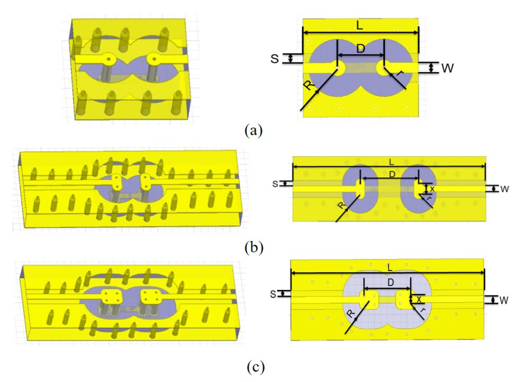
Figure 1 shows the proposed redundant RF TSV. Figure 1b,c are dual and quad redundant RF TSVs on high resistivity Si substrate, respectively, while Figure 1a is a traditional single RF TSV as a reference. For ease of use in further test and S-parameters extraction, RF TSVs on high resistivity Si substrate are connected by coplanar waveguide (CPW) lines, which have a designed impedance of 50 Ω and dimensions are summarized in Table 1.
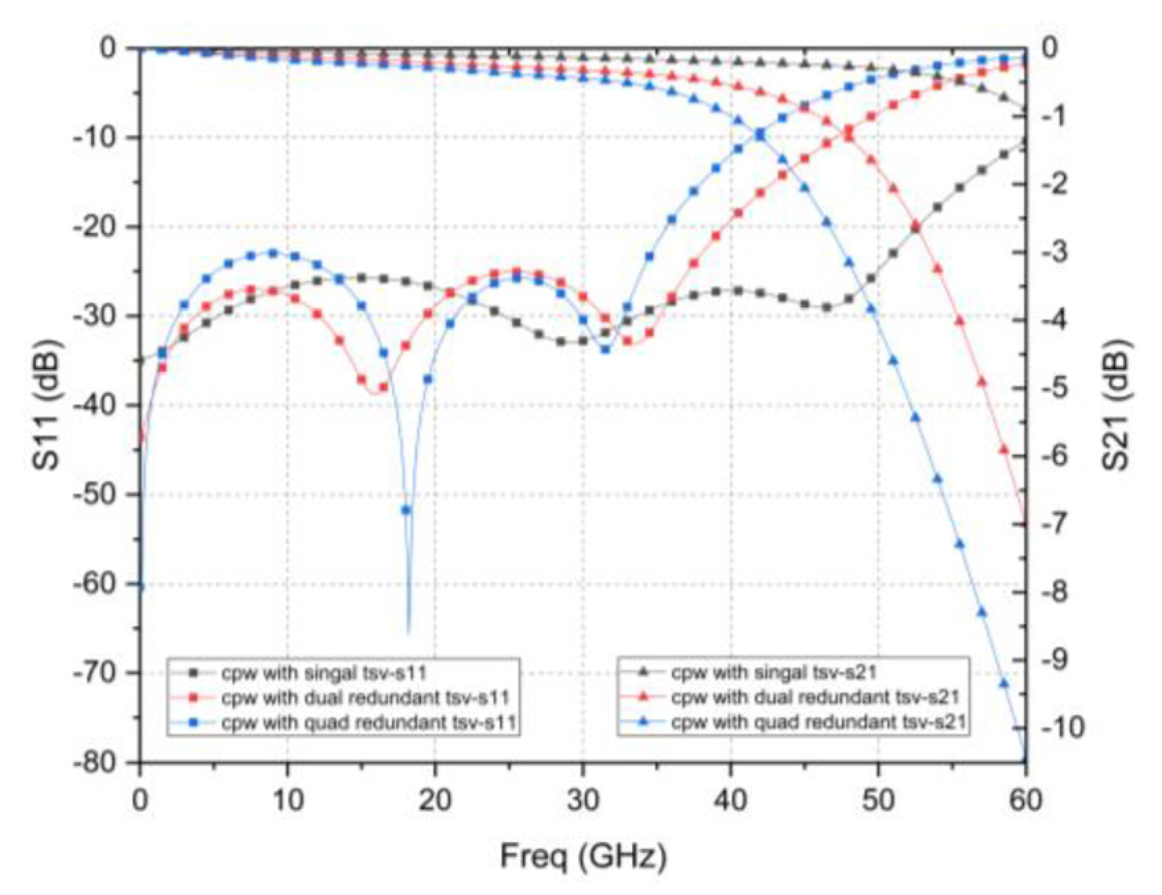
Figure 2 shows simulated S-parameters with HFSS model. It can be seen that at a frequency of 40 GHz, the insertion losses of a single TSV interconnect test structure, dual redundant TSV interconnect test structure, and quad redundant TSV interconnect test structure design are 0.197 dB, 0.538 dB, and 0.998 dB, respectively. The S11 parameter is less than −15 dB. The results show that it has a good high-frequency transmission performance. At the same time, as the number of redundant TSVs increases, the S21 parameter shows that the insertion loss value gradually degrades, and the S11 parameter shows that the resonance frequency gradually decreases.
To better understand the effect of the redundant TSVs on the high-frequency transmission performance, a modified lumped circuit model is established for the dual redundant TSV test structure in this paper, as shown in Figure 3. The parameters of the symbols in the model are listed in Table 2. The values of each lumped element can be calculated by applying the dimensions [22,23,24,25] and material properties [26,27,28] in the following equations. The diameter, width, length, thickness, height, and spacing is symbolized d, w, l, t, h, and p, respectively.
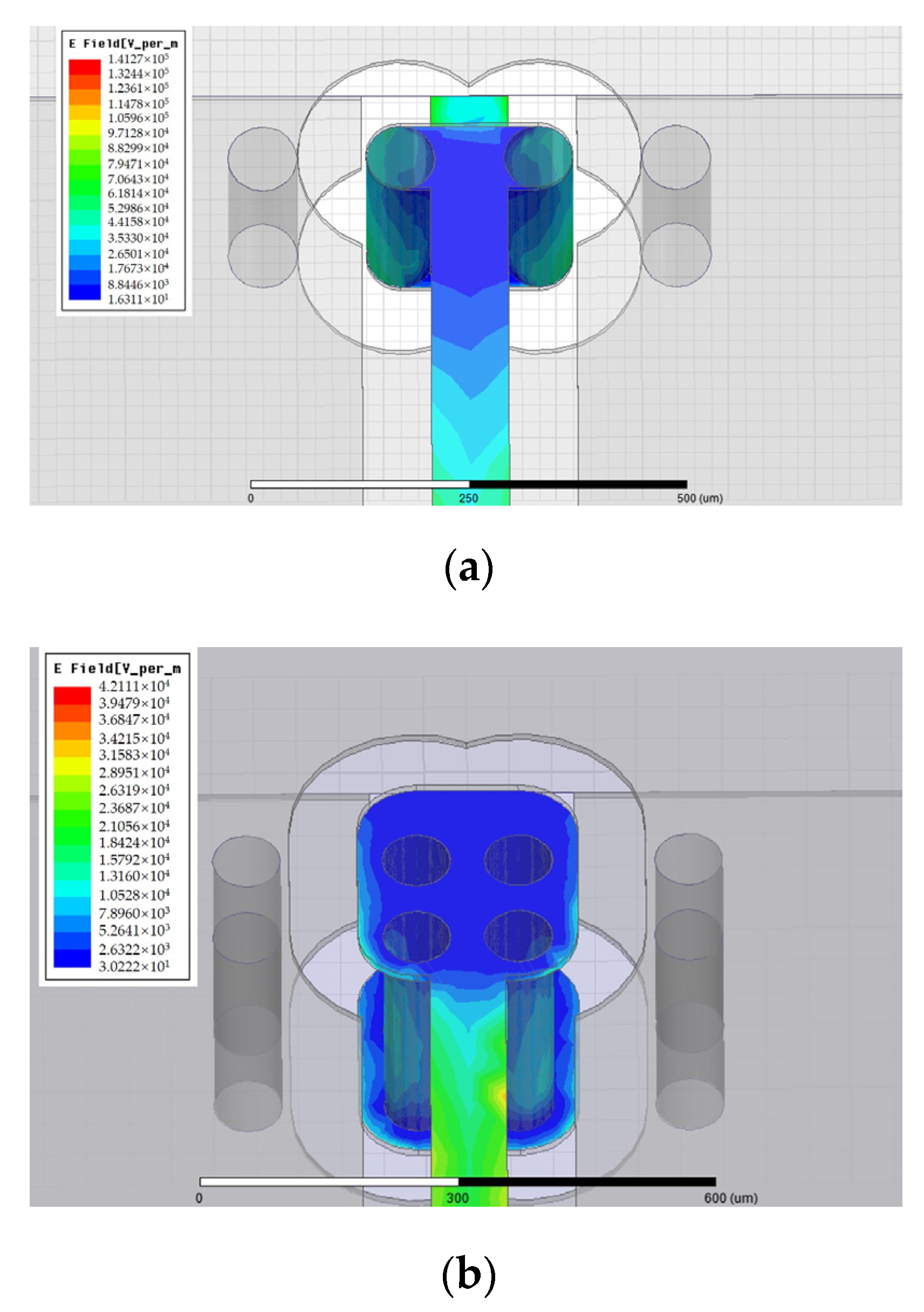
When the alternating current in the same direction flows in the redundant TSV copper column, the alternating magnetic field generated by each current will generate eddy currents on adjacent TSVs, resulting in uneven current distribution in the TSV copper column and the proximity effect. The electric field distribution of the redundant TSV design proposed in this paper is shown in Figure 4. It is obvious that the internal electric field of TSV is concentrated in the edge area. Therefore, the equivalent resistance and inductance of TSV are changed, which needs to be considered when calculating the equivalent circuit.
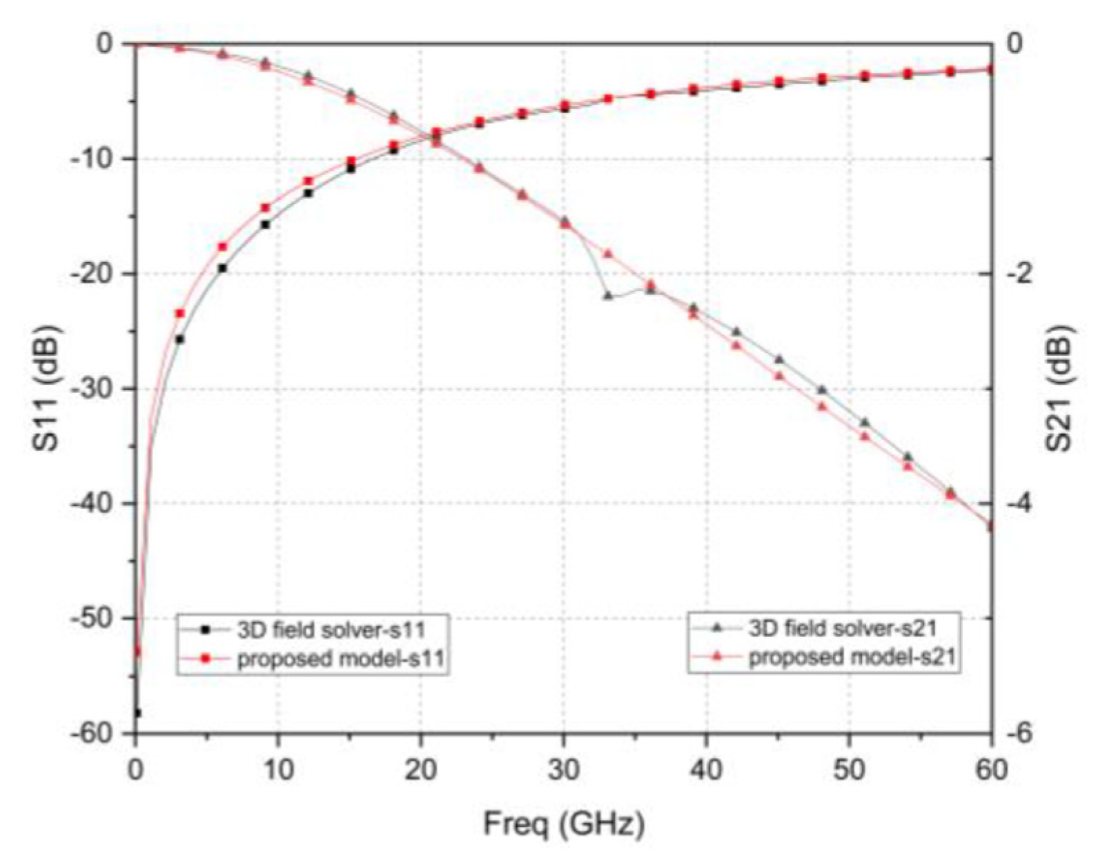
The simulation results with HFSS and the established equivalent circuit model in Figure 3 are shown in Figure 5. The similarity of the curvature of the amplitude curves of S11 and S21 indicates that the establishment of the equivalent circuit model is correct. It can be seen from the equivalent circuit model that, at high frequencies, the main factors that affect the S-parameters are inductance and resistance. As the redundant structure contains multiple RF TSVs, the proximity effect between TSVs will increase, and the overall inductance and resistance will increase due to the additional RDL required to connect multiple TSVs. Therefore, an increase in the number of redundant TSVs will cause the resonance frequency to appear in the lower frequency range, and the high-frequency loss will degrade significantly.
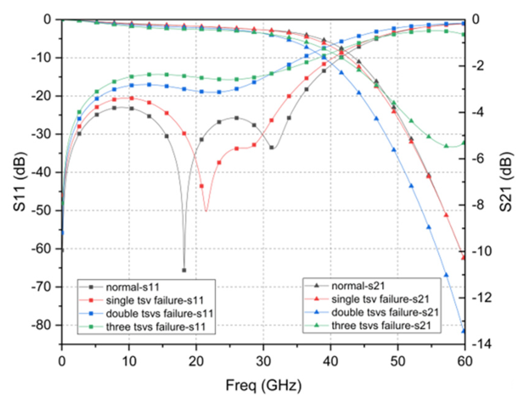
In order to verify the feasibility of the RF redundant TSV scheme, Figure 6 and Figure 7 shows that the S-parameters of dual and quad redundant RF TSV test structure when failure occurs. It can be found that it has a higher resonance frequency and smaller insertion loss as the number of failed TSV increases. This result is basically consistent with the above analysis. Furthermore, it can achieve reliable function at 0–44 GHz regardless of what failure occurs.
3. Fabrication
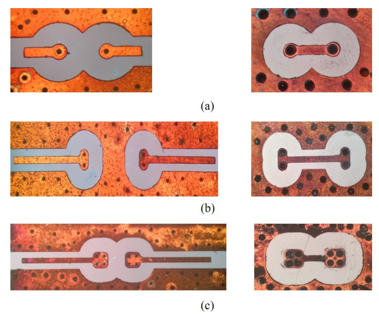
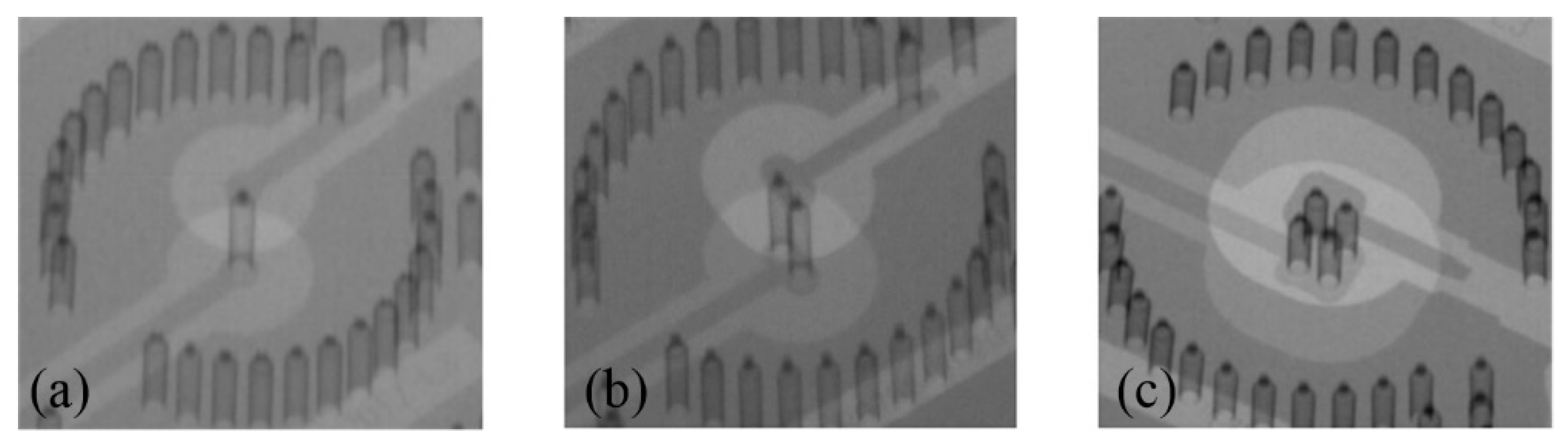
Figure 8 shows the main steps for fabricating the redundant RF TSV sample. They include the following: (a) First, a 300 μm high-resistance silicon wafer is cleaned in acetone and isopropanol. (b) The fabrication of the large backside TSV is completed by photolithography and deep reactive ion etching. (c) The fabrication of the small front side TSV is completed by back engraving and deep reactive ion etching. (d) After standard cleaning, a high-temperature thermal oxygen process is used to form a dense 100 nm SiO2 insulating layer on the surface of the high resistance silicon wafer and the sidewall of the TSV. (e) The double-sided sputtered adhesion layer Ti and seed layer Cu is fabricated. (f) Double-sided lithography and thickening of the surface local copper layer and TSV hole copper layer is conducted by electroplating in a copper sulfate solution. (g) Copper plating area mask protection is carried out. Removing the excess Cu seed layer and Ti adhesion layer by wet etching. (h) Electroless nickel-gold plating is con-ducted on the Cu layer. Figure 9 provides a physical diagram of the completed production. As shown in Figure 10, the metal filling in the TSV hole is good under X-ray detection. To extract the S-parameters of the TSV interconnect structure, a transmission line is also manufactured at the same wafer.
4. RF Test and Analysis
The redundant RF TSV samples were tested using a GSG probe in a semi-automatic probe station, which was connected with an AV3629 high-performance microwave integrated vector network analyzer. Before the test, the measurement system was firstly calibrated using the classic SOLT calibration method, including short circuit, open circuit, load, and straight through four standard structures, to correct the system error, stripping probe and cable parasitic parameters [29]. The measured insertion losses at 40 GHz for a single TSV interconnect test structure, dual redundant TSV interconnect test structure, and quad redundant TSV interconnect test structure are 0.721 dB, 1.18 dB, and 1.635 dB, respectively.
Compared with the simulation results in Section 2, the maximum deviations of the insertion loss of the simulation and testing of a single TSV, dual redundant TSV and four redundant TSV test structures are 0.53 dB, 0.84 dB, and 0.95 dB in the range of 0–40 GHz, which may be caused by the use of the ideal Cu layer in the simulation. However, the fabricated Cu layer has some differences with ideal Cu layer, such as surface roughness and resistivity. Figure 11 is a captured photo of the Cu layer by a profiler during the process, which shows the roughness is approximately 60–70 nm and some local regions reach about 150 nm due to oxidation. Table 3 summarizes the tested resistivity, which has an average resistivity of 12.79 μΩ·cm. Because surface roughness of the copper generates parasitic inductance, the surface impedance will change and results in conductor loss [30]. Especially when the skin depth corresponding to the operating frequency is less than or equal to the surface roughness, the effect of surface roughness will become very significant [31,32]. Additionally, the resistivity of the conductor also affects the conductor loss. To testify this point, using the monitored data, the simulation is optimized and repeated in HFSS model, and the results are compared with the test results shown in Figure 12. It can be seen that the deviation is relatively reduced, and the higher the frequency, the better the fit. This proves that the roughness and resistivity of the conductor have an impact on high-frequency performance. It can also be seen in the figure that the gap between the measured and simulated results of the four-redundancy is significantly larger compared to a single TSV. Since the resistivity and roughness of the conductor in the hole cannot be measured, the parameters of the conductor on the plane can only be used instead. As the number of RF TSV holes increases, the error accumulation is greater.
5. S-Parameter Extraction
To obtain the precise value of insertion loss contributed by RF redundant TSVs, de-embedding was conducted. According to the relevant theory of microwave network parameters, conversion into ABCD parameters with cascade characteristics for RF redundant TSV sample structures was carried out via parameter transformation and matrix operation [33]. The 1000 μm CPW test structure is viewed as four 250 μm CPW connections. A single RF TSV interconnect and redundant RF TSV interconnect test structure is viewed as three CPW and two TSV interconnect structures, as shown in Figure 13. To simplify the description, J1, J2, J3, and J4 are used to represent the CPW, single TSV interconnect, dual redundant TSV interconnect, and quad redundant TSV interconnect test structure. L1 represents 250 μm CPW and S-TSV represents a single TSV mutual connected structure, D-TSV represents a dual redundant TSV interconnect structure, and Q-TSV represents a quad redundant TSV interconnect structure.
The ABCD parameters corresponding to the four unit structures are represented by square brackets “[]” and the tag name. The ABCD parameters of the unit structure are multiplied by the unit structure to represent the ABCD parameters of the three test structures J1, J2, J3, and J4 as
The number of frequency points of the high-frequency measurement is marked as N, and the size of the ABCD parameters matrix of all the above test structures and unit structures is 2 × 2 × N. In the calculation, an N-step loop is set to perform a 2 × 2 matrix operation. The de-embedding process solves a single TSV interconnect S-TSV, a dual redundant TSV interconnect D-TSV, and a quad-redundant TSV interconnect Q-TSV using the above four matrix equations. Through the operations of square root and inversion matrix, the ABCD parameters matrix of each unit structure is obtained as
where [L2] is an intermediate variable for simplifying expressions. According to the transformation relationship between ABCD parameters and S-parameters, the ABCD parameters of each unit structure is converted into S-parameters, and the transmission characteristics of the three TSV interconnections can be compared. Microwave network parameter conversion and other operations in the de-embedding process are performed in MATLAB software(MATLAB, R2020a, MathWorks, Natick, Mass, USA).
Using the above de-embedding process, the S-parameters of the two kinds of RF TSV design are obtained, as shown in Figure 14. It can be observed that the S21 values of the three TSV interconnects are close when the frequency is less than 40 GHz, and the gap is in the range of 0.25 dB. When the frequency is greater than 40 GHz, the S21 value of the dual redundant and quad-redundant TSV interconnects degrade rapidly versus frequency, and the insertion loss of the quad-redundant TSV interconnect significantly increases. The test results of the TSV interconnection and the simulation results of the equivalent lumped components models are compared. The following points can be seen from Figure 14: (a) The simulated and measured insertion loss values gradually degrade as frequency increases. (b) Both simulation and measurement results show a similar trend that the insertion loss value degrades as the number of RF Redundant TSV increase. (c) The S-parameter curve of the TSV interconnection extracted from the RF measurement results shows some fluctuation, bringing out maximum deviation values of 0.07 dB, 0.17 dB, and 0.12 dB in the 0–40 GHz range between the simulation and measured results for a single TSV, dual redundant TSV, and four redundant TSV respectively. These fluctuations should be ascribed to the surface roughness or random discontinuities in the deposited Cur layer on the sidewall of TSV, of which, the later one is especially hard to discern or characterize to our knowledge. This is the reason why the current simulation based equivalent lumped component circuit model only considers the change of conductor resistivity as well. However, even with the deviations due to the fluctuations, those founding is sufficient to draw a conclusion that it has a competing RF property with single RF TSV for Redundant RF design, which is the most important to this research and highlighted in the Table 4 as well.
At present, there is no report of RF redundant TSV interconnection sample measurement result, although few papers proposed RF redundant RF TSV design. Table 4 compares redundant RF TSVs proposed in this paper with single TSV products presented in recent years. It can be seen from the table that when the frequency is less than 40 GHz, the RF Redundant TSV interconnection sample fabricated in this work is in the same level with traditional single RF TSV in term of RF insertion loss, but it has a better capacity to resist failure risk of RF TSVs.
6. Conclusions
This paper presented a RF redundant TSV design for a high resistance Si interposer as a package substrate. To verify the feasibility of the scheme, two test structures for connecting CPW transmission lines through redundant TSVs were designed to be able to work in 0–40 GHz. Modeling and simulation were carried out using HFSS, conclusion can be drawn from the obtained S-parameters that the more the number of RF redundant TSV, the lower the resonance frequency, and the greater the insertion loss. This was also solidified with the results obtained with the established modified equivalent circuit model for RF redundant TSV interconnection. The simulation also shows that the designed RF redundant TSV interconnection is capable to work in the range of 0–40 GHz without unacceptable RF property degradation when failure occurs. RF redundant TSV test vehicles were fabricated and tested, while an improved simulation factoring in nonideal factors such as surface roughness and resistivity is also taken. The result of the test shows an agreement with simulation. The tested insertion loss of the single TSV, dual redundant TSV and quad redundant TSV after de-embedding is 0.22, 0.19, and 0.46 dB at 40 GHz, respectively, which is close to the reported single TSV design. However, redundant TSV offers a better capacity to resist failure risk of TSV.
Author Contributions
Conceptualization, S.M. and Y.J.; Methodology, S.M.; Software, S.H. and M.W.; Validation, L.H., S.M., and Y.J.; Formal Analysis, S.M.; Investigation, L.H. and S.M.; Resources, J.C. and W.W.; Data Curation, S.H. and M.W.; Writing—original draft preparation, M.W.; Writing–Review & Editing, S.M.; Visualization, M.W.; Supervision, S.M.; Project Administration, L.H., S.M., and Y.J.; Funding Acquisition, L.H., S.M., and Y.J. All authors have read and agreed to the published version of the manuscript.
Funding
This research was funded by the National Natural Science Foundation of China, no. U1613215. This research was also funded by TSV 3D Integrated Micro/Nano system lab, ZDSYS201802061805105.
Institutional Review Board Statement
Not applicable.
Informed Consent Statement
Not applicable.
Data Availability Statement
The data presented in this study are available on request from the corresponding author. The data are not publicly available due to the experimental data needs to be further researched in the future.
Conflicts of Interest
The authors declare no conflict of interest.
References
- Talebbeydokhti, P.; Dalmia, S.; Thai, T.; Sover, R.; Tal, S. Ultra large area SIPs and integrated mmW antenna array module for 5G mmWave outdoor applications. In Proceedings of the 2019 IEEE 69th Electronic Components and Technology Conference (ECTC), Las Vegas, NV, USA, 29–30 May 2019; pp. 294–299. [Google Scholar] [CrossRef]
- Hu, S.; Wang, L.; Xiong, Y.-Z.; Lim, T.G.; Zhang, B.; Shi, J.; Yuan, X. TSV Technology for millimeter-wave and terahertz design and applications. IEEE Trans. Compon. Packag. Manuf. Technol. 2010, 1, 260–267. [Google Scholar] [CrossRef]
- Yan, J.; Ma, S.; Jin, Y.; Wang, W.; Chen, J.; Luo, R.; Cai, H.; Li, J.; Xia, Y.; Hu, L.; et al. Fabrication and RF property evaluation of high-resistivity Si interposer for 2.5-D/3-D heterogeneous integration of RF devices. IEEE Trans. Compon. Packag. Manuf. Technol. 2018, 8, 2012–2020. [Google Scholar] [CrossRef]
- El Bouayadi, O.; Dussopt, L.; Lamy, Y.; Dehos, C.; Ferrandon, C.; Siligaris, A.; Soulier, B.; Simon, G.; Vincent, P. Silicon interposer: A versatile platform towards full-3D integration of wireless systems at millimeter-wave frequencies. In Proceedings of the 2019 IEEE 69th Electronic Components and Technology Conference (ECTC), Las Vegas, NV, USA, 29–30 May 2019; pp. 973–980. [Google Scholar]
- Lamy, Y.; Dussopt, L.; El Bouayadi, O.; Ferrandon, C.; Siligaris, A.; Dehos, C.; Vincent, P. A compact 3D silicon interposer package with integrated antenna for 60GHz wireless applications. In Proceedings of the 2013 IEEE International 3D Systems Integration Conference (3DIC), Francisco, CA, USA, 2–4 October 2013. [Google Scholar]
- Thadesar, P.A.; Bakir, M.S. Fabrication and characterization of polymer-enhanced TSVs, inductors, and antennas for mixed-signal silicon interposer platforms. IEEE Trans. Compon. Packag. Manuf. Technol. 2016, 6, 455–463. [Google Scholar] [CrossRef]
- Sekhar, V.N.; Toh, J.S.; Cheng, J.; Sharma, J.; Fernando, S.; Bangtao, C.; Fernando, S. Wafer level packaging of RF MEMS devices using TSV interposer technology. In Proceedings of the 2012 IEEE 14th Electronics Packaging Technology Conference (EPTC), Singapore, 5–7 December 2012. [Google Scholar]
- Tenailleau, J.-R.; Brunet, A.; Borel, S.; Voiron, F.; Bunel, C. TSV development, characterization and modeling for 2.5-D interposer applications. In Proceedings of the 2013 IEEE 63rd Electronic Components and Technology Conference, Las Vegas, NV, USA, 28–31 May 2013. [Google Scholar]
- Xu, Z.; Lu, J.Q. Three-dimensional coaxial through-silicon-via (TSV) design. IEEE Electron Device Lett. 2012, 10, 1441–1443. [Google Scholar] [CrossRef]
- Yu, P.; Lin, H.; He, Z.; Song, C.; Cai, J.; Wang, Q.; Wang, Z. Coaxial through-silicon-vias using low-κ SiO2 insulator. In Proceedings of the 2020 IEEE 70th Electronic Components and Technology Conference (ECTC), Orlando, FL, USA, 3–30 June 2020. [Google Scholar]
- Hwang, G.; Kalaiselvan, R.; Sam, M.I.E.; Hsiang-Yao, H. Study on through Silicon Via (TSV) filling failures on various electroplating conditions. In Proceedings of the 2019 IEEE 21st Electronics Packaging Technology Conference (EPTC), Singapore, 4–6 December 2019. [Google Scholar]
- Hollman, R.; Dimov, O.; Malik, S.; Hichri, H.; Arendt, M. Ultra fine RDL structure fabrication using alternative patterning and bottom-up plating processes. In Proceedings of the 2018 IEEE 68th Electronic Components and Technology Conference (ECTC), San Diego, CA, USA, 29 May–1 June 2018. [Google Scholar]
- Murugesan, M.; Fukushima, T.; Mori, K.; Nakamura, A.; Lee, Y.; Motoyoshi, M.; Bea, J.; Watariguchi, S.; Koyanagi, M. Fully-filled, highly-reliable fine-pitch interposers with TSV aspect ratio >10 for future 3D-LSI/IC packaging. In Proceedings of the 2019 IEEE 69th Electronic Components and Technology Conference (ECTC), Las Vegas, NV, USA, 25 May–2 June 2019. [Google Scholar]
- Bleiker, S.J.; Fischer, A.C.; Shah, U.; Somjit, N.; Haraldsson, T.; Roxhed, N.; Oberhammer, J.; Stemme, G.; Niklaus, F. High-aspect-ratio through silicon vias for high-frequency application fabricated by magnetic assembly of gold-coatednickel wires. IEEE Trans. Compon. Packag. Manuf. Technol. 2015, 5, 21–27. [Google Scholar] [CrossRef]
- Liu, X.; Chen, Q.; Dixit, P.; Chatterjee, R.; Tummala, R.R.; Sitaraman, S.K. Failure mechanisms and optimum design for electroplated copper Through-Silicon Vias (TSV). In Proceedings of the 2009 59th Electronic Components and Technology Conference, San Diego, CA, USA, 26–29 May 2009. [Google Scholar]
- Shen, J.; Chen, P.; Su, L.; Shi, T.; Tang, Z.; Liao, G. X-ray inspection of TSV defects with self-organizing map network and Otsu algorithm. Microelectron. Reliab. 2016, 67, 129–134. [Google Scholar] [CrossRef]
- Kang, U.; Chung, H.J.; Heo, S.; Park, D.H.; Lee, H.; Kim, J.H.; Ahn, S.H.; Cha, S.H.; Ahn, J.; Kwon, D.; et al. 8Gb 3D DDR3 DRAM using through-silicon-via technology. IEEE J. Solid State Circuits 2009, 45, 130–131. [Google Scholar]
- Hsieh, A.-C.; Hwang, T. TSV Redundancy: Architecture and design issues in 3-D IC. IEEE Trans. Very Large Scale Integr. Syst. 2011, 20, 711–722. [Google Scholar] [CrossRef]
- Jiang, L.; Xu, Q.; Eklow, B. On effective TSV repair for 3D-stacked ICs. In Proceedings of the Design, Automation and Test in Europe Conference and Exhibition (DATE), Dresden, Germany, 12–16 March 2012. [Google Scholar]
- Ma, S.; Chai, Y.; Yan, J.; Cai, H.; Hu, L.; He, S.; Wang, W.; Chen, J.; Jin, Y. A 2.5D integrated L band receiver based on high resistivity Si interposer. In Proceedings of the 2018 IEEE International Conference on Integrated Circuits, Technologies and Applications (ICTA), Beijing, China, 21–23 November 2018. [Google Scholar]
- Rahimi, A.; Somarajan, P.; Yu, Q. Modeling and characterization of through-silicon-vias (TSVs) in radio frequency regime in an active interposer technology. In Proceedings of the 2020 IEEE 70th Electronic Components and Technology Conference (ECTC), Lake Buena Vista, FL, USA, 26–29 May 2020. [Google Scholar]
- Lu, K.-C.; Horng, T.-S. Wideband and scalable equivalent-circuit model for differential through silicon vias with measurement verification. In Proceedings of the 2013 IEEE 63rd Electronic Components and Technology Conference, Las Vegas, NV, USA, 28–31 May 2013. [Google Scholar]
- Jung, D.H.; Kim, Y.; Kim, J.J.; Kim, H.; Choi, S.; Song, Y.-H.; Bae, H.-C.; Choi, K.-S.; Piersanti, S.; De Paulis, F.; et al. Through silicon via (TSV) defect modeling, measurement, and analysis. IEEE Trans. Compon. Packag. Manuf. Technol. 2016, 7, 138–152. [Google Scholar] [CrossRef]
- Leferink, F.B.J. Inductance calculations; methods and equations. In Proceedings of the International Symposium on Electromagnetic Compatibility, Atlanta, GA, USA, 14–18 August 1995; IEEE ISEMC. 1995; pp. 16–22. [Google Scholar]
- Kim, J.; Pak, J.S.; Cho, J.; Song, E.; Cho, J.; Kim, H.; Song, T.; Lee, J.; Lee, H.; Park, K.; et al. High-frequency scalable electrical model and analysis of a through silicon Via (TSV). IEEE Trans. Compon. Packag. Manuf. Technol. 2011, 1, 181–195. [Google Scholar]
- Hassan, M.D.; Farque, M.R.I. Left-handed metamaterial using Z-shaped SRR for multiband application by azimuthal angular rotationsm. Mater. Res. Express. 2017, 4, 045801. [Google Scholar] [CrossRef]
- Hassan, M.D.; Faruque, M.R.I.; Islam, S.S.; Islam, M.T. New compact double-negative miniaturized metamaterial for wideband operation. Materials 2016, 9, 830. [Google Scholar] [CrossRef] [PubMed] [Green Version]
- Hasan, M.; Faruque, M.R.I.; Islam, M.T. Compact left-handed meta-atom for S-, C- and Ku-band application. Appl. Sci. 2017, 7, 1071. [Google Scholar] [CrossRef] [Green Version]
- Ye, R.; Xu, J. SOLT calibration method and its application to radio-frequency measurement. Chin. J. Electron Devices 2006, 29, 179. [Google Scholar]
- Chen, C.D.; Tzuang, C.K.; Peng, S.T. Full-wave analysis of a lossy rectangular waveguide containing rough inner surfaces. IEEE Microw. Guided Wave Lett. 1992, 2, 180–181. [Google Scholar] [CrossRef]
- Palasantzas, G. Influence of self-affine and mound roughness on the surface impedance and skin depth of conductive materials. J. Phys. Chem. Solids 2004, 65, 1271–1275. [Google Scholar] [CrossRef] [Green Version]
- Scogna, A.C.; Schauer, M. Performance analysis of strip line surface roughness models. In Proceedings of the International Symposium on Electromagnetic Compatibility, Detroit, MI, USA, 18–22 August 2008. [Google Scholar]
- Noyan, K.; Aksun, M.I. Modern Microwave Circuits; Artech House: Boston, MA, USA, 2008; pp. 58–68. [Google Scholar]
- Khan, W.T.; Tong, J.; Sitaraman, S.; Sundaram, V.; Tummala, R.; Papapolymerou, J. Characterization of electrical properties of glass and transmission lines on thin glass up to 50 GHz. In Proceedings of the 2015 IEEE 65th Electronic Components and Technology Conference (ECTC), San Diego, CA, USA, 26–29 May 2015. [Google Scholar]
- Chung, D.J.; Bhattacharya, S.K.; Papapolymerou, J. Low loss multilayer transitions using via technology on LCP from DC to 40 GHz. In Proceedings of the 2009 59th Electronic Components and Technology Conference, San Diego, CA, USA, 26–29 May 2009. [Google Scholar]
- Chen, B.; Sekhar, V.N.; Jin, C.; Lim, Y.Y.; Toh, J.S.; Fernando, S.; Sharma, J. Low-loss broadband package platform with surface passivation and TSV for wafer-level packaging of RF-MEMS devices. IEEE Trans. Compon. Packag. Manuf. Technol. 2013, 3, 1443–1452. [Google Scholar] [CrossRef]
- Ebefors, T.; Fredlund, J.; Perttu, D.; Van Dijk, R.; Cifola, L.; Kaunisto, M.; Rantakari, P.; Vaha-Heikkila, T. The development and evaluation of RF TSV for 3D IPD applications. In Proceedings of the 2013 IEEE International 3D Systems Integration Conference (3DIC), Francisco, CA, USA, 2–4 October 2013. [Google Scholar]
- Lorival, J.E.; Calmon, F.; Sun, F.; Frantz, F.; Plossu, C.; Le Berre, M.; O’Connor, I.; Valorge, O.; Charbonnier, J.; Henry, D.; et al. An efficient and simple compact modeking approach for 3-D interconnects with IC’s stack global electrical context consideration. Microelectron. J. 2015, 46, 153–165. [Google Scholar] [CrossRef]
- Kim, N.; Wu, D.; Kim, D.; Rahman, A.; Wu, P. Interposer design optimization for high frequency signal transmission in passive and active interposer using through silicon via (TSV). In Proceedings of the 2011 IEEE 61st Electronic Components and Technology Conference (ECTC), Lake Buena Vista, FL, USA, 31 May–3 June 2011. [Google Scholar]
Figure 1.
Test structure HFSS model: (a) single TSV; (b) dual redundant TSV; (c) quad redundant TSV.
Figure 1.
Test structure HFSS model: (a) single TSV; (b) dual redundant TSV; (c) quad redundant TSV.

Figure 2.
Test structure simulation result.

Figure 3.
Equivalent circuit models of dual redundant TSV test structure.

Figure 4.
Electric field diagram: (a) dual redundant TSV; (b) quad redundant TSV.

Figure 5.
S-parameters results of dual redundant TSV structure obtained by 3D FEM solver and equivalent circuit model.
Figure 5.
S-parameters results of dual redundant TSV structure obtained by 3D FEM solver and equivalent circuit model.

Figure 6.
Dual redundant TSV failure simulation results.

Figure 7.
Quad redundant TSV failure simulation results.

Figure 8.
Process design.

Figure 9.
Test structure physical photo: (a) single TSV; (b) dual redundant TSV; (c) quad redundant TSV.
Figure 9.
Test structure physical photo: (a) single TSV; (b) dual redundant TSV; (c) quad redundant TSV.

Figure 10.
Test structure X-ray detection map: (a) single TSV; (b) dual redundant TSV; (c) quad redundant TSV.
Figure 10.
Test structure X-ray detection map: (a) single TSV; (b) dual redundant TSV; (c) quad redundant TSV.

Figure 11.
Surface roughness test results: (a) small roughness area; (b)large roughness area.

Figure 12.
Test structure S21 parameter measurement results and optimized simulation results of HFSS.
Figure 12.
Test structure S21 parameter measurement results and optimized simulation results of HFSS.

Figure 13.
Schematic diagram of test structure de-embedding.

Figure 14.
TSV interconnects S21 parameter measurement results and simulation results of the equivalent lumped components models: (a) S11; (b) S21.
Figure 14.
TSV interconnects S21 parameter measurement results and simulation results of the equivalent lumped components models: (a) S11; (b) S21.


Table 1.
Parameters of the test structure (μm).
| Table 1 | L | S | W | D | R | r | x |
|---|---|---|---|---|---|---|---|
| Single TSV | 1000 | 70 | 100 | 400 | 250 | 75 | - |
| Dual redundant TSV | 3000 | 70 | 100 | 400 | 250 | 75 | 160 |
| Quad redundant TSV | 3000 | 70 | 100 | 640 | 250 | 75 | 120 |
Table 2.
Symbols and parameters in the equivalent circuit model for TSV and RDL.
| Symbol | Parameter |
|---|---|
| RRDL/RTSV | Resistance of RDL/TSV |
| LRDL | Self-Inductance of RDL |
| LTSVclosed | Inductance of RDL under the influence of proximity effect |
| CRDLinSub/Csub | Capacitance between RDL/TSV and substrate |
| GRDLinSub/Gsub | Conductance between RDLs/TSVs in silicon substrate |
| PF | Proximity effect correction factor |
| dCu | Skin depth |
Table 3.
Resistivity test results.
| Points | Resistivity/μΩ·cm |
|---|---|
| 1 | 4.56 |
| 2 | 12.44 |
| 3 | 13.95 |
| 4 | 12.43 |
| 5 | 18.24 |
| 6 | 12.36 |
| Average value | 12.79 |
Table 4.
Comparison RF TSV for high frequency applications.
| Ref. | Substrate Material | Type of Vias | Transmission Loss of One Transition (dB) | Via Size (μm) | Via Length (μm) | |
|---|---|---|---|---|---|---|
| 10 GHz | 40 GHz | |||||
| [34] | Glass | Single TGV | 0.03 | 0.22 | Φ55 | 366 |
| [35] | LCP | Single Via | 0.071 | 0.12 | Φ55 | 51 |
| [36] | Si(HR) | Single TSV | 0.05 | — | Φ100 | 300 |
| [37] | Si(HR) | Single TSV | 0.04 | — | Φ8 & Φ90 | 25 & 280 |
| [38] | Si(HR) | Single TSV | 1.6 | — | Φ40 | 120 |
| [39] | Si(HR) | Single TSV | 0.37 | — | Φ10 | 100 |
| This Work | Si(HR) | Single TSV | 0.11 | 0.22 | Φ40 & Φ80 | 50 & 250 |
| Dual redundant TSV | 0.14 | 0.19 | ||||
| Quad redundant TSV | 0.2 | 0.46 | ||||
Publisher’s Note: MDPI stays neutral with regard to jurisdictional claims in published maps and institutional affiliations. |
© 2021 by the authors. Licensee MDPI, Basel, Switzerland. This article is an open access article distributed under the terms and conditions of the Creative Commons Attribution (CC BY) license (http://creativecommons.org/licenses/by/4.0/).
Share and Cite
MDPI and ACS Style
Wang, M.; Ma, S.; Jin, Y.; Wang, W.; Chen, J.; Hu, L.; He, S. A RF Redundant TSV Interconnection for High Resistance Si Interposer. Micromachines 2021, 12, 169. https://0-doi-org.brum.beds.ac.uk/10.3390/mi12020169
AMA Style
Wang M, Ma S, Jin Y, Wang W, Chen J, Hu L, He S. A RF Redundant TSV Interconnection for High Resistance Si Interposer. Micromachines. 2021; 12(2):169. https://0-doi-org.brum.beds.ac.uk/10.3390/mi12020169
Chicago/Turabian StyleWang, Mengcheng, Shenglin Ma, Yufeng Jin, Wei Wang, Jing Chen, Liulin Hu, and Shuwei He. 2021. "A RF Redundant TSV Interconnection for High Resistance Si Interposer" Micromachines 12, no. 2: 169. https://0-doi-org.brum.beds.ac.uk/10.3390/mi12020169
Note that from the first issue of 2016, this journal uses article numbers instead of page numbers. See further details here.