
Surface-Potential-Based Compact Modeling of p-GaN Gate HEMTs
by
 , , ,
, , ,
Jie Wang
1 ,
,
Zhanfei Chen
1,*,
Shuzhen You
2,
Benoit Bakeroot
3,
Jun Liu
1 and
Stefaan Decoutere
2 1
The Key Laboratory for RF Circuit and Systems of Ministry of Education, Hangzhou Dianzi University, Hangzhou 310012, China
2
Interuniversity Microelectronics Centre (IMEC), Kapeldreef 75, B-3001 Leuven, Belgium
3
CMST, IMEC, Ghent University, Technologiepark 126, B-9052 Ghent, Belgium
*
Author to whom correspondence should be addressed.
Micromachines 2021, 12(2), 199; https://0-doi-org.brum.beds.ac.uk/10.3390/mi12020199
Submission received: 20 January 2021
/
Revised: 4 February 2021
/
Accepted: 13 February 2021
/
Published: 15 February 2021
(This article belongs to the Special Issue GaN-Based Semiconductor Devices)
Abstract
:We propose a surface potential (SP)-based compact model of p-GaN gate high electron mobility transistors (HEMTs) which solves the Poisson equation. The model includes all possible charges in the GaN channel layer, including the unintended Mg doping density caused by out-diffusion. The SP equation and its analytical approximate solution provide a high degree of accuracy for the SP calculation, from which the closed-form I–V equations are derived. The proposed model uses physical parameters only and is implemented in Verilog-A code.
1. Introduction
GaN based high electron mobility transistors (HEMTs), which are typically normally-on devices, draw significant attention for power switching applications due to the combined merits of a high OFF-state voltage and low ON-resistance RON originating from the high electron mobility and large breakdown electric field in these materials [1]. Yet the market demands for normally-off or enhancement mode (E-mode) devices. One of the approaches to obtain E-mode transistors is to use a p-GaN gate that lifts up the conduction band at the channel surface in equilibrium [2] and results in normally-off operation [3] by depleting the 2-D electron gas (2DEG) in the channel [4]. Today, the p-GaN gate devices were the first commercialized E-mode devices with high and robust threshold voltage Vth, high breakdown voltage, and low dynamic RON increase [5].
Effective circuit design using these devices requires fast and accurate models that can describe the behavior of the device under different working conditions. Previous work includes models such as the Curtice model [6], the Statz model [7], and the Angelov–Chalmers model [8], which are mostly empirical curve-fitting models that might not work well for large signal operation. DynaFET [9] is an innovative nonlinear model based on a non-linear network analyzer (NVNA) and an artificial neural network (ANN). These models hardly represent the physical GaN HEMT behavior, for they lack any predictive capability and are strictly limited to the test system. To overcome these difficulties, an exact, complete, and simple physics-based model is required. Two industrial standard models were recently selected by the CMC (Compact Model Council). First, there is the ASM model [10], a physics-based surface-potential (SP) model able to capture terminal characteristics of GaN HEMTs by solving the Schroedinger–Poisson coupled equations. Secondly, unlike SP-based models, the MIT Virtual Source GaN (MVSG) model [11] formulates mobile charge densities through a threshold voltage term. The physics-based MVSG model adopts a different interpretation of the carrier velocity by using an empirical saturation function for GaN HEMTs. Recently, a charge-based HEMT model was developed by EPFL [12], starting from a physics-based model for regular silicon FETs and was given new physical quantities typical for HEMTs. However, the above models lack the physics of the typical gate structure in the p-GaN gate HEMTs, consisting of a “back-to-back” diode configuration [13].
Previously, we have developed a SP-based model for Schottky gate GaN HEMTs [14] which solved the problem of elaborate computations of the surface potential by using an approximate analytical solution. The goal of this work is to extend our model of the p-GaN HEMTs, by considering within the Poisson equation all possible charges induced: the polarization charges at the AlGaN/GaN and p-GaN/AlGaN interfaces, the active Mg doping in the AlGaN barrier and the GaN channel caused by out-diffusion [4], and holes. Our SP-based model is physics-based and precisely captures all operation regions in the Direct Current (DC) behavior. The model accuracy was demonstrated by the excellent agreement between the model and experimental data including Current–Voltage (I-V) and Capacitance–Voltage (C-V) results. The p-GaN gate HEMT model was implemented in Verilog-A, and the main characteristics of the device can be reproduced.
This brief is arranged as follows: In Section II, we present the device structure. Section III is divided in two subsections: (1) we describe the drain current (ID) and gate current (IG) models and (2) the gate, drain, and source charges are calculated. The model’s implementation, parameter extraction, and experimental validation are discussed in Section IV. Finally, we conclude this paper.
2. Device Structure
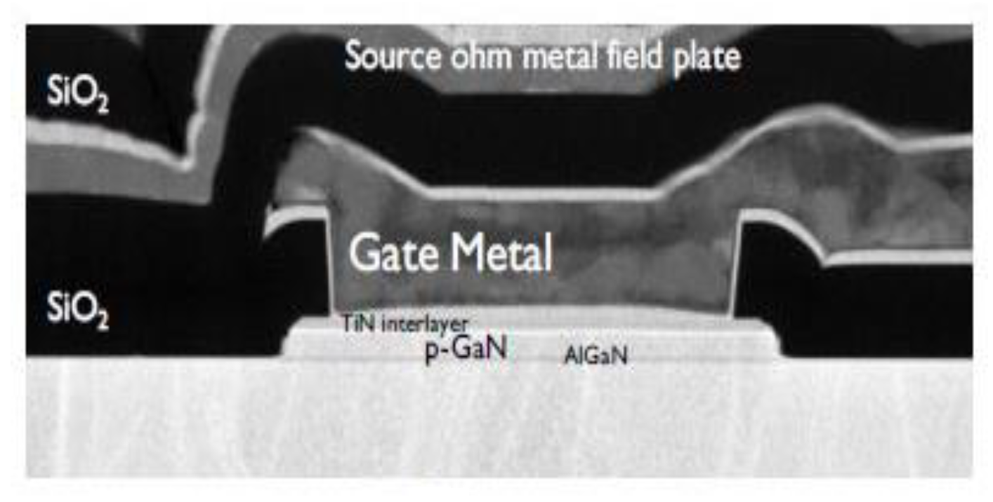
The p-GaN gate HEMTs were fabricated in 200 mm pilot line using an Au-free process flow. Details of the process flow are described in [4]. Figure 1 shows a cross-section transmission electron microscope (TEM) picture of the gate area of a realized p-GaN gate HEMT. Table 1 is the main material properties in p-GaN gate HEMT.
3. Surface Potential (SP)-Based Model
3.1. Current Calculation
First of all, it is important to concentrate on modeling the potential distribution along the channel of the p-GaN gate HEMTs. In order to obtain the electrostatic potential distribution in the p-GaN gate HEMTs, the 1D Poisson equation is solved in the GaN channel layer, in which the carrier density is determined by the polarization charges and the p-GaN gate at equilibrium [2]. Additionally, the p-GaN HEMTs feature unintended Mg doping density in the channel caused by out-diffusion, and thus the Poisson equation, including all possible charges within the device, must be considered. Since both the AlGaN and GaN layers are usually undoped, the depletion charge can be neglected. For completeness, we included hole charge density in the Poisson equation:
where εGaN is the permittivity of GaN, NMg is the unintended Mg doping in the channel caused by out-diffusion, φ is the surface potential, x is the direction along channel width, y is the direction perpendicular to the channel, nGaN and pGaN are the electrons’ and holes’ charge densities in the GaN channel layer, respectively.
The nGaN and pGaN are written as:
The nGaN and pGaN can be represented in terms of the intrinsic carrier concentration ni, the Fermi potential ΦF (ΦF = VT[ln(N/ni)+2−1.5(N/ni)]; N is the carrier concentration), the thermal voltage VT (VT = kT/q), and the voltage VC applied between the channel and the substrate.
If we assume the gradual channel approximation that ignores the lateral field gradient in the Poisson equation, that is, ignore the y dependence of (x; y) in Equation (1), then we get:
Defining a Gaussian surface from the GaN channel down to the neutral substrate gives the potential at x: φ(x) = 0 for x → ∞ and dφ(x)/dx = 0 for x → ∞. Imposing these boundary conditions gives, at x = 0, φ(x = 0) = φGaN at the surface, where φGaN is the surface potential.
With the two-order integral from φ = 0 to φ = φGaN of Equation (4), we can get the Surface-Potential Equation (SPE) shown in Equation (5), and this is the basis for our model.
In Equation (5), VG is the gate voltage; γ is the body factor; V0 is a fitting parameter such that the surface potential φGaN equals zero when VG = V0. We use an advanced non-iterative algorithm [15] to solve Equation (5) in a self-consistent way and obtain the potential distribution along the surface.
The surface potential φpGaN at the p-GaN/AlGaN layer interface is calculated with the same methodology [15].
where εpGaN is the permittivity of AlGaN; is the Mg doping in the p-GaN layer; npGaN and ppGaN are the electrons’ and holes’ charge densities in the p-GaN layer, respectively.
The drain current is the most important device parameter of the HEMT device. The model uses drift-diffusion transport to calculate the drain current and adopts the channel current equation of the thin layer charge model [16] as:
where ID is the drain current, qi is the charge density in the GaN channel, μ is the electron mobility, and W is the gate width.
The p-GaN gate HEMTs, fabricated at IMEC, feature a TiN gate metal on top of the p-GaN layer in order to form a Schottky contact on the p-GaN to 2DEG gate input diode, to reduce the leakage current. Therefore, the gate leakage follows a path along this “back-to-back diode” structure [2].
According to the “back-to-back” diodes structure in the p-GaN gate HEMTs, the Schottky junction is reverse biased while the p-GaN/AlGaN/GaN junction is forward biased for higher gate voltages. The gate current can be calculated from the thermionic emission (TE) current over the AlGaN/GaN heterojunction with the current continuity condition [17]:
where Area is the area of the gate, JTE0 is the current density of heterojunction which depends on the AlGaN/GaN barrier height, T is the temperature, and nTE is the ideality factor for heterojunction.
At VG < 0 V, the Schottky junction is forward biased, while the p-GaN/AlGaN/GaN junction is reverse biased, and the gate current is determined by a reverse leakage current along the edges of the gate and across the heterojunction. For this reverse leakage current, the hopping transport (HT) [18] model has been developed. The gate current empirically obeys the following equation:
where Peri is the perimeter of the gate, JHT0 is the reverse saturation current density, nHT is the ideality factor, and α is the temperature coefficient [19].
3.2. Charge Calculation
The gate, drain, and source charges can be calculated by integrating the channel charge (qch) along the channel following the Ward–Dutton charge partitioning [20] as:
where L is the channel length, W is the channel width and x is the position along the channel.
The integration in Equation (10) can be solved using the Symmetric Linearization Method [21] and neglecting the effect of velocity saturation on the charge.
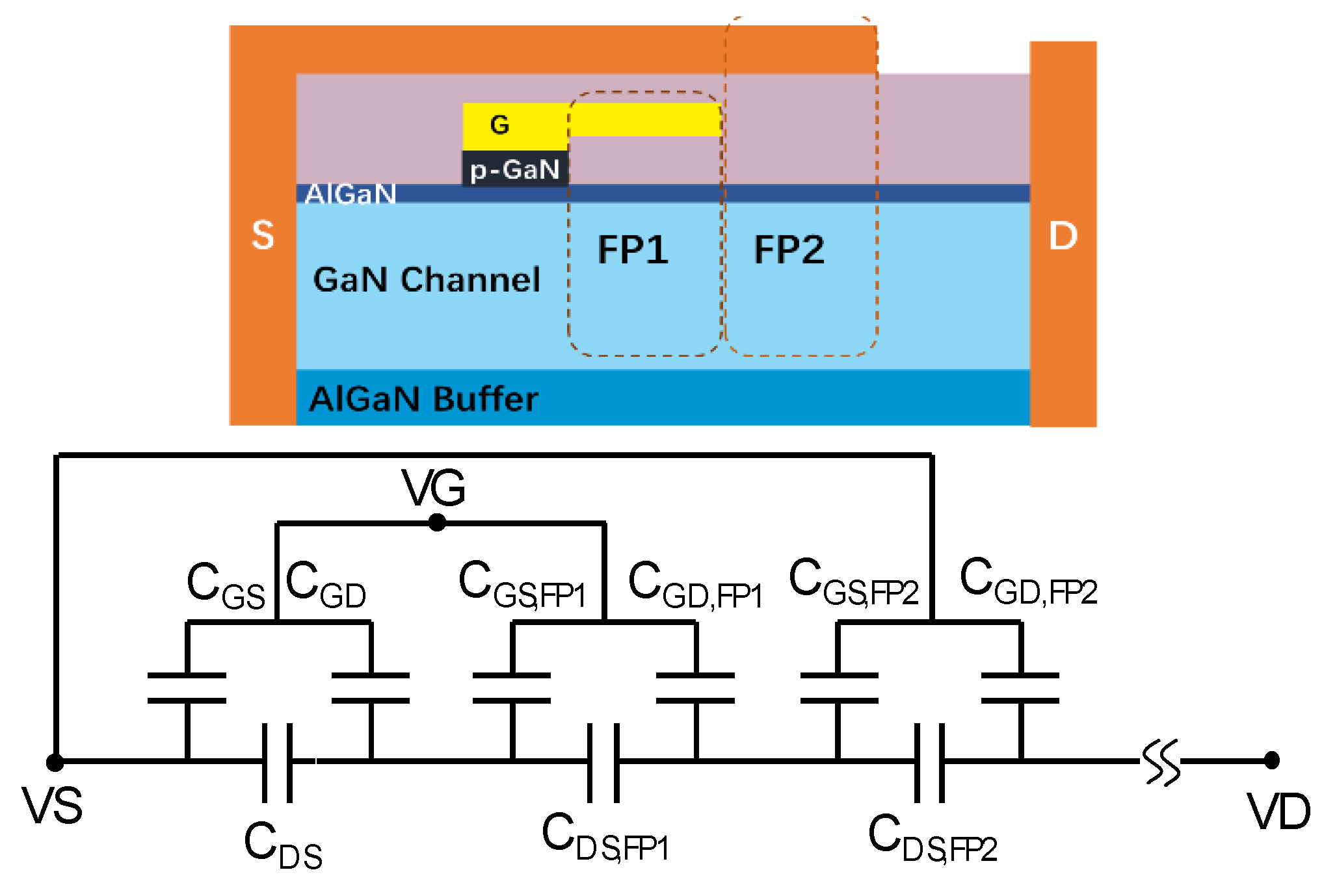
The complete p-GaN gate HEMT structure contains several field plates (FPs), and therefore, attention is given to the accurate modeling of the FPs within the device. Given the field plate configuration depicted in Figure 2, the 2DEG is present below the FP at equilibrium. These field plate regions can be regarded as additional transistors in series with different threshold voltages. Hence, the field plate regions can be regarded as additional transistors in series with different operating voltages. The C–V behavior of a p-GaN gate HEMT is of utmost importance for the high-frequency performance and switching characteristics of these high-power devices, and this is intrinsically related to the FP configuration. The equivalent circuit of capacitances is shown in Figure 2. The C–V characteristics can be modeled considering the capacitors with varying insulator thickness.
4. Results and Discussion
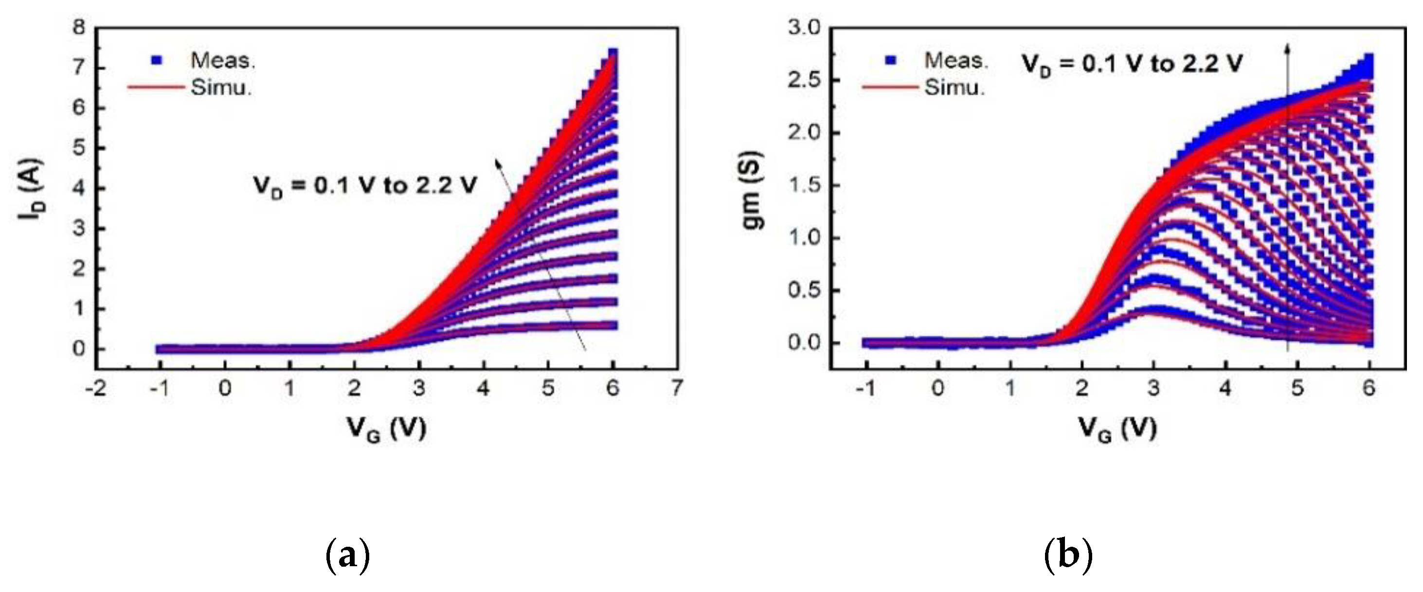
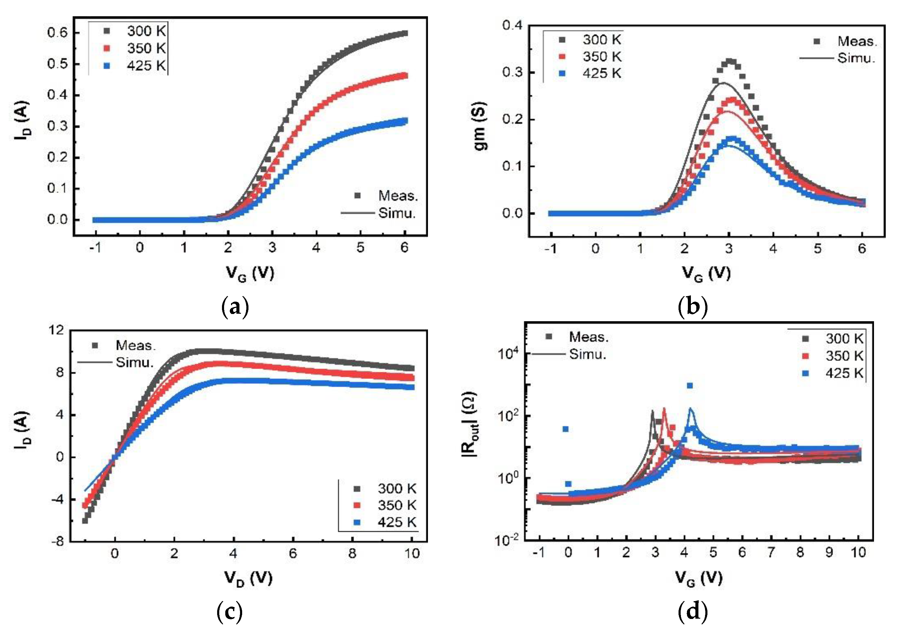
We have validated the proposed SP-based compact model using I–V and C–V measurement data of a typical 200 V p-GaN gate high-power HEMT device with a total device width W of 36 mm. The model is in good agreement with the measured currents, especially the gate current, and capacitances, as shown in Figure 3, Figure 4, Figure 5, Figure 6 and Figure 7. For transconductance characteristics in Figure 3b, the effect of high electric field is lack in this model, which will be considered in the follow-up work to improve the accuracy.
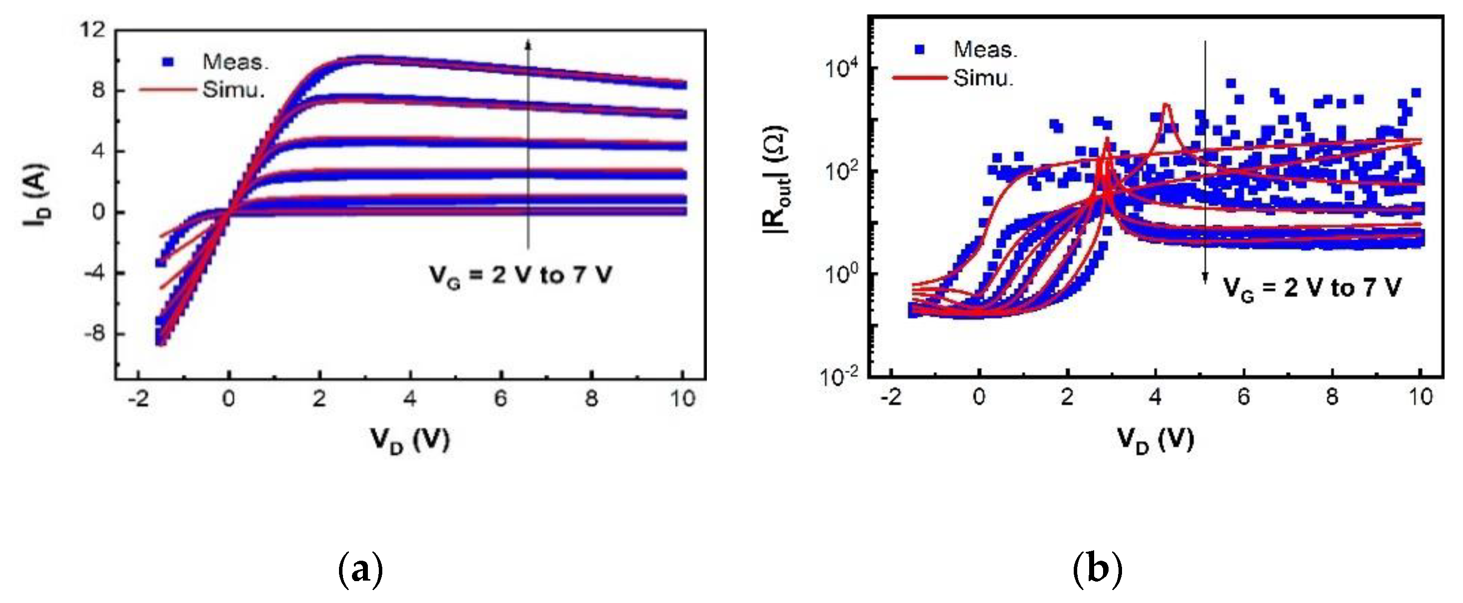
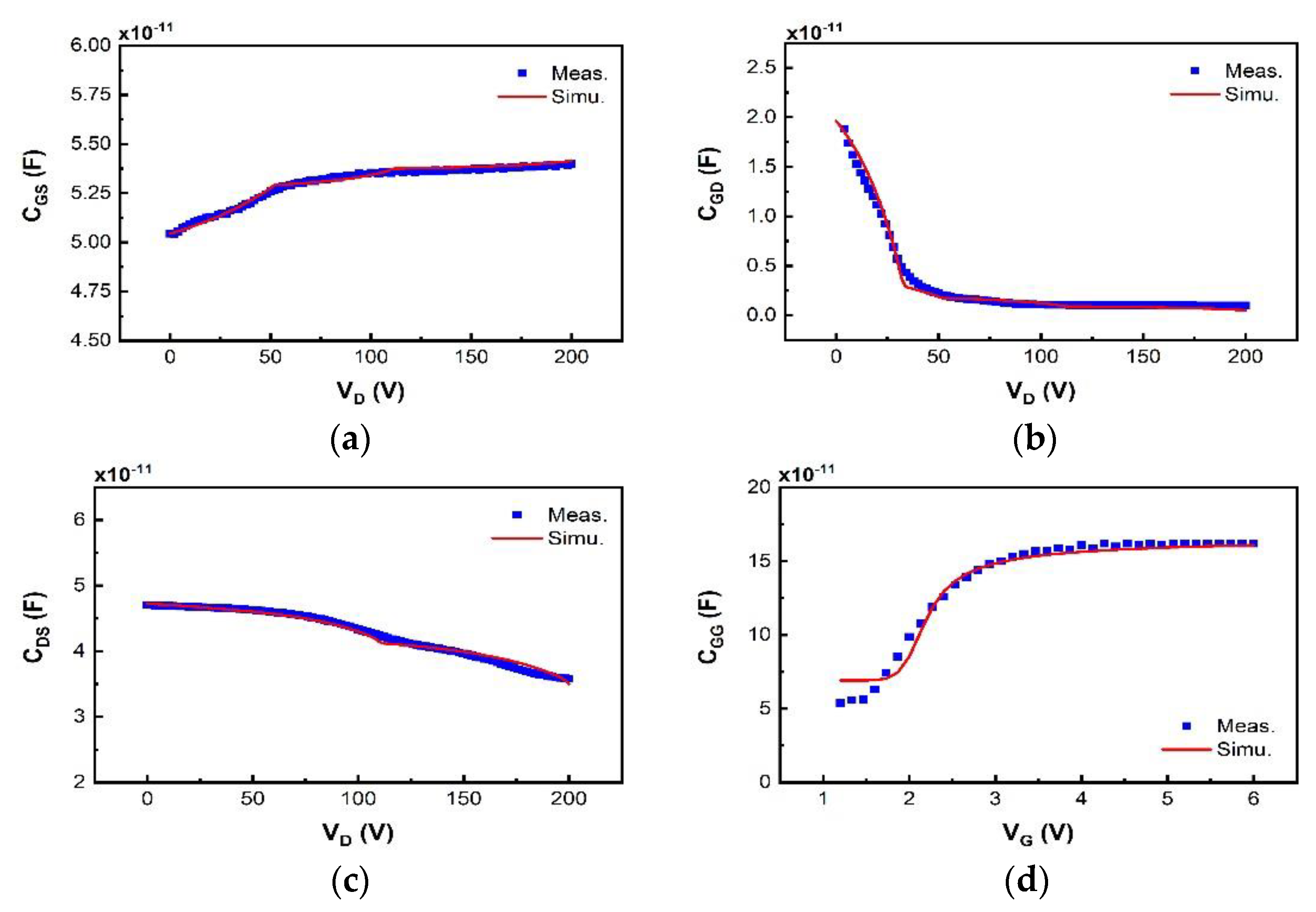
The simulated transfer and output characteristics match well with the measurement results at 300 K in Figure 3 and Figure 4, sweeping VG from −1 V to 6 V with VD from 0.1 V to 2.2 V in ID-VG, and VD from −1 V to 10 V with VG from 2 V to 7 V in ID-VD. The OFF-state capacitances CGS, CGD, and CDS at VG = 0 V with VD from 0 V to 200 V, are nicely modeled in Figure 5, capturing the impact of the field plates that modulate the 2DEG distribution at high VD. The developed compact SP-based model successfully reproduces the measured current and capacitance characteristics.
The temperature dependence characteristics are also modelled and shown in Figure 6.
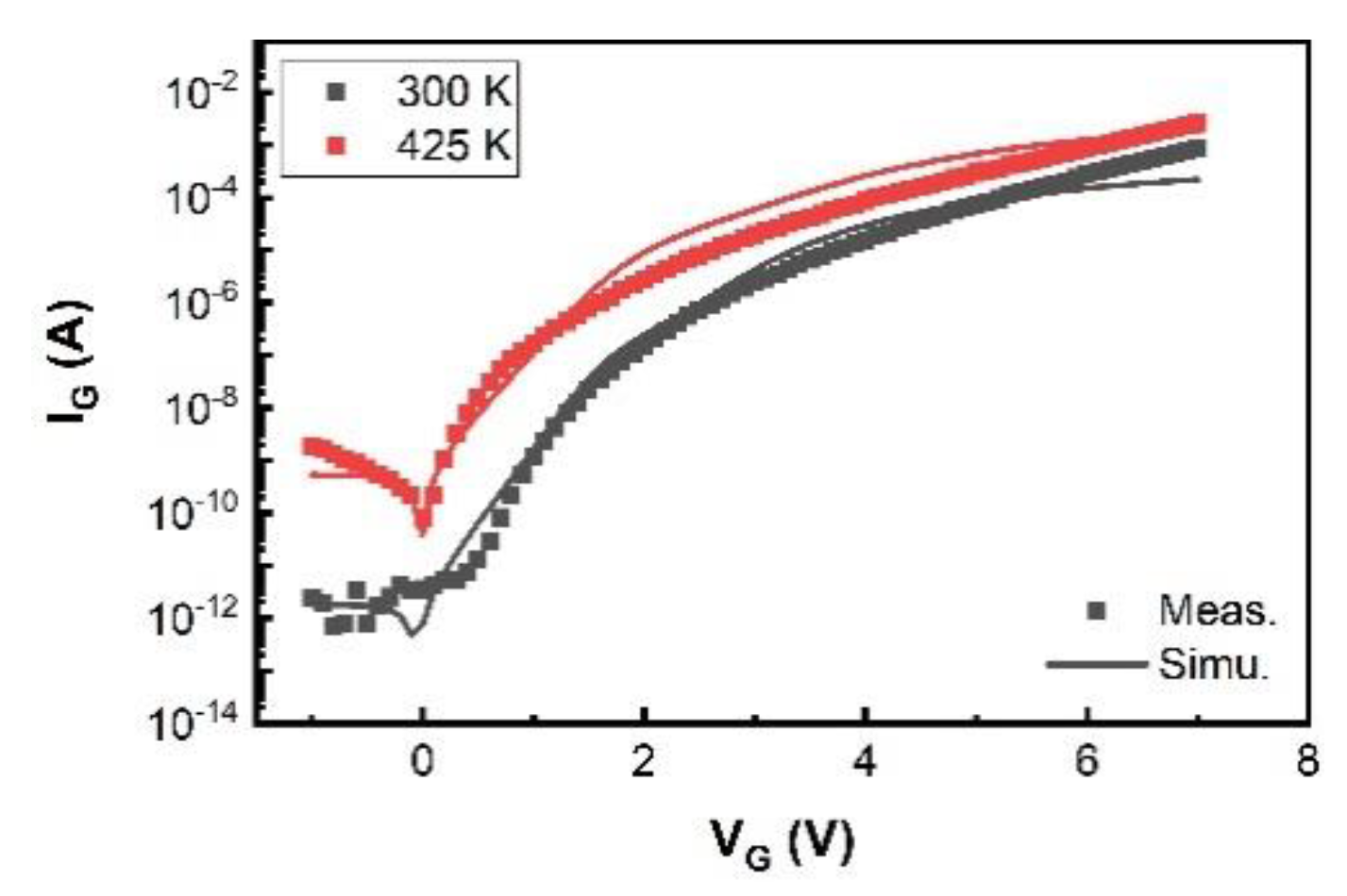
The Figure 7 shows an excellent agreement between the model and the measurement for both branches of VG ≥ 0 V and VG < 0 V at different temperatures of 300 and 425 K.
5. Conclusions
The proposed SP-based compact model for p-GaN gate HEMTs is based on a surface-potential analytical approximate solution, which considers all possible induced charges at the AlGaN/GaN interface. This model gets the complete potential distribution along the surface by solving the Poisson equation. The developed compact model is physical as it includes the main GaN HEMT features in the solution of the Poisson equation. Good fit to the measurement results was obtained over a large range of gate and drain voltages. It was verified that this model can reproduce all observed current and capacitance characteristics of p-GaN gate HEMTs automatically.
Author Contributions
Writing—original draft preparation, J.W. and Z.C.; writing—review and editing, S.Y., B.B., J.L., and S.D. All authors have read and agreed to the published version of the manuscript.
Funding
This research was funded by the National Natural Science Foundation of China, grant number 61871161, and the Zhejiang Province Natural Science Foundation, grant number LZ17F010001.
Conflicts of Interest
The authors declare no conflict of interest.
References
- Mishra, U.K.; Parikh, P.; Wu, Y.-F. AlGaN/GaN HEMTs-an overview of device operation and applications. Proc. IEEE 2020, 90, 1022–1031. [Google Scholar] [CrossRef] [Green Version]
- Bakeroot, B.; Stockman, A.; Posthuma, N.; Stoffels, S.; Decoutere, S. Analytical Model for the Threshold Voltage of p-(Al)GaN High-Electron-Mobility Transistors. IEEE Trans. Electron Devices 2018, 65, 79–86. [Google Scholar] [CrossRef]
- Marcon, D.; Saripalli, Y.N.; Decoutere, S. 200 mm GaN-on-Si epitaxy and e-mode device technology. In Proceedings of the 2015 IEEE International Electron Devices Meeting (IEDM), Washington, DC, USA, 7–9 December 2015. [Google Scholar]
- Posthuma, N.E.; You, S.; Liang, H.; Ronchi, N.; Kang, X.; Wellekens, D.; Saripalli, Y.N.; Decoutere, S. Impact of Mg out-diffusion and activation on the p-GaN gate HEMT device performance. In Proceedings of the 28th International Symposium on Power Semiconductor Devices and ICs (ISPSD), Prague, Czech Republic, 12–16 June 2016. [Google Scholar]
- Walter, R. Curtice. Nonlinear modeling of compound semiconductor HEMTs state of the art. In Proceedings of the IEEE MTT-S International Microwave Symposium Digest, Anaheim, CA, USA, 23–28 May 2010. [Google Scholar]
- Chen, K.J.; Oliver, H.; Alex, L.; Chun, L.T.; Tetsuzo, U.; Yasuhiro, U.; Wu, Y.F. GaN-on-Si Power Technology: Devices and Applications. IEEE Trans. Electron Devices 2017, 64, 779–795. [Google Scholar] [CrossRef]
- Statz, H.; Newma, P.; Smith, I.W. GaAs FET device and circuit simulation in SPICE. IEEE Trans. Electron Devices 1987, 34, 160–165. [Google Scholar] [CrossRef]
- Angelov, I.; Zirath, H.; Rosman, N. A new empirical nonlinear model for HEMT and MESFET devices. Microw. Theory Technol. 1992, 40, 2258–2261. [Google Scholar] [CrossRef] [Green Version]
- Xu, J.; Jones, R.; Harris, S.A.; Nielsen, T.; Root, D.E. Dynamic FET Model-DynaFET-for GaN Transistors from NVNA Active Source Injection Measurements. In Proceedings of the IEEE MTT-S International Microwave Symposium Digest, Tampa, FL, USA, 1–6 June 2014. [Google Scholar]
- Ghosh, S.; Ahsan, S.A.; Dasgupta, A.; Khandelwal, S.; Chauhan, Y.S. GaN HEMT modeling for power and RF applications using ASM-HEMT. In Proceedings of the 2016 3rd International Conference on Emerging Electronics (ICEE), Mumbai, India, 27–30 December 2016. [Google Scholar]
- Radhakrishna, U. Modeling Gallium-Nitride Based High Electron Mobility Transistors: Linking Device Physics to High Voltage and High Frequency Circuit Design. Ph.D. Thesis, Department of Electrical Engineering and Computer Science, Massachusetts Institute of Technology, Cambridge, MA, USA, 2016. [Google Scholar]
- Jazaeri, F.; Sallese, J.M. Charge-Based EPFL HEMT Model. IEEE Trans. Electron Devices 2019, 66, 1218–1229. [Google Scholar] [CrossRef]
- Stoffels, S.; Bakeroot, B.; Wu, T.L.; Marcon, D.; Posthuma, N.E.; Decoutere, S.; Tallarico, A.N.; Fiegna, C. Failure mode for p-GaN gates under forward gate stress with varying Mg concentration. In Proceedings of the IEEE International Reliability Physics Symposium (IRPS), Monterey, CA, USA, 2–6 April 2017. [Google Scholar]
- Wang, J.; Sun, L.; Liu, J.; Zhou, M. A surface-potential-based model for AlGaN/AlN/GaN HEM. J. Semicond. 2013, 34, 0002–0007. [Google Scholar] [CrossRef]
- Wang, J. Study on the Surface Potential-Based Model of GaN HEMT. Ph.D. Thesis, Department of Electrical Engineering, Zhejiang University, Hangzhou, China, 2013. [Google Scholar]
- Brews, J.R. A Charge-Sheet Model of the MOSFET. Solid -State Electron 1978, 21, 345–355. [Google Scholar] [CrossRef]
- Rhoderick, E.H.; Williams, R.H. Current-transport mechanisms. In Metal-Semiconductor Contacts, 2nd ed.; Clarendon: Oxford, UK, 1988; pp. 98–100. [Google Scholar]
- Zhao, L.; Chen, L.; Yu, G.; Yan, D.; Yang, G.; Liu, B.; Gu, X.; Lu, H. Tunneling-Hopping Transport Model for Reverse Leakage Current in InGaN/GaN Blue Light-Emitting Diodes. IEEE Photonics Technol. Lett. 2017, 29, 1447–1450. [Google Scholar] [CrossRef]
- Wang, J.; Chen, Z.; You, S.; Benoit, B.; Liu, J.; Sun, L.; Decoutere, S. Surface-Potential-Based Compact Model for the Gate Current of p-GaN Gate HEMTs. IEEE Trans. Electron Devices 2020, 67, 3564–3567. [Google Scholar] [CrossRef]
- Oh, S.Y.; Ward, D.E.; Dutton, R.W. Transient analysis of mos transistors. IEEE Trans. Electron Devices 1980, 27, 1571–1578. [Google Scholar]
- Gildenblat, G.; Li, X.; Wu, W.; Wang, H.; Jha, A.; van Langevelde, R.; Smit, G.D.J.; Scholten, A.J.; Klaassen, D.B.M. PSP: An Advanced Surface-Potential-Based MOSFET Model for Circuit Simulation. IEEE Trans. Electron Devices 2006, 53, 1979–1993. [Google Scholar] [CrossRef]
Figure 1.
Transmission electron microscope(TEM) picture of the Schottky metal/p-GaN gate AlGaN/GaN high electron mobility transistors (HEMT).
Figure 1.
Transmission electron microscope(TEM) picture of the Schottky metal/p-GaN gate AlGaN/GaN high electron mobility transistors (HEMT).

Figure 2.
The equivalent circuit of the capacitance of field plates (FPs) of a p-GaN gate HEMT.

Figure 3.
Measurement data (dots) and simulation data (line) at 300 K with VD from 0.1 to 2.2 V, step = 0.1 V. (a) Transfer characteristics; (b) transconductance characteristics.
Figure 3.
Measurement data (dots) and simulation data (line) at 300 K with VD from 0.1 to 2.2 V, step = 0.1 V. (a) Transfer characteristics; (b) transconductance characteristics.

Figure 4.
Measurement data (dots) and simulation data (line) at 300 K with VG from 2 to 7 V, step = 1 V. (a) Output characteristics; (b) absolute values of output resistance characteristics.
Figure 4.
Measurement data (dots) and simulation data (line) at 300 K with VG from 2 to 7 V, step = 1 V. (a) Output characteristics; (b) absolute values of output resistance characteristics.

Figure 5.
The C–V characteristics of the surface potential (SP) model (line) are compared with measurement data (dot) as a function of input voltage: (a) CDS at different VD; (b) CGD at different VD; (c) CGS at different VD; (d) CGG (= CGS + CGD) at different VG.
Figure 5.
The C–V characteristics of the surface potential (SP) model (line) are compared with measurement data (dot) as a function of input voltage: (a) CDS at different VD; (b) CGD at different VD; (c) CGS at different VD; (d) CGG (= CGS + CGD) at different VG.

Figure 6.
Measurement data (dots) and simulation data (line) at different temperatures. (a) Transfer characteristics with VD = 0.1 V; (b) transconductance resistance characteristics with VD = 0.1 V; (c) output characteristics with VG = 7 V; (d) output resistance characteristics with VG = 7 V.
Figure 6.
Measurement data (dots) and simulation data (line) at different temperatures. (a) Transfer characteristics with VD = 0.1 V; (b) transconductance resistance characteristics with VD = 0.1 V; (c) output characteristics with VG = 7 V; (d) output resistance characteristics with VG = 7 V.

Figure 7.
Measurement (dots) and simulation (lines) data of IG at 300 and 425 K with VDS = 0.1 V.


Table 1.
Main material properties in p-GaN gate HEMT.
| Parameter | Physical Meaning | p-GaN HEMT |
|---|---|---|
| NMg | Mg density | 3~5 × 1017 cm−3 |
| Eg-GaN | GaN Band gap | 3.4 eV |
| ∆EC | The Difference between the Conductor Bottom and Fermi Level | 0.518 eV |
| NC | GaN Conduction band density | 2.02 × 1018 cm−3 |
| NV | GaN Valence band density | 9.08 × 1018 cm−3 |
| εGaN | GaN dielectric constant | 9.4 |
| εAlGaN | AlGaN dielectric constant | 8.94 |
Publisher’s Note: MDPI stays neutral with regard to jurisdictional claims in published maps and institutional affiliations. |
© 2021 by the authors. Licensee MDPI, Basel, Switzerland. This article is an open access article distributed under the terms and conditions of the Creative Commons Attribution (CC BY) license (http://creativecommons.org/licenses/by/4.0/).
Share and Cite
MDPI and ACS Style
Wang, J.; Chen, Z.; You, S.; Bakeroot, B.; Liu, J.; Decoutere, S. Surface-Potential-Based Compact Modeling of p-GaN Gate HEMTs. Micromachines 2021, 12, 199. https://0-doi-org.brum.beds.ac.uk/10.3390/mi12020199
AMA Style
Wang J, Chen Z, You S, Bakeroot B, Liu J, Decoutere S. Surface-Potential-Based Compact Modeling of p-GaN Gate HEMTs. Micromachines. 2021; 12(2):199. https://0-doi-org.brum.beds.ac.uk/10.3390/mi12020199
Chicago/Turabian StyleWang, Jie, Zhanfei Chen, Shuzhen You, Benoit Bakeroot, Jun Liu, and Stefaan Decoutere. 2021. "Surface-Potential-Based Compact Modeling of p-GaN Gate HEMTs" Micromachines 12, no. 2: 199. https://0-doi-org.brum.beds.ac.uk/10.3390/mi12020199
Note that from the first issue of 2016, this journal uses article numbers instead of page numbers. See further details here.