Automatic Configurable Hardware Code Generation for Software-Defined Radios †


Software Defined Radio Group, Electrical Engineering Department, University of Cape Town, Cape Town 7701, South Africa
*
Author to whom correspondence should be addressed.
†
This paper is an extended version of our paper published in the International Conference on Field Programmable Technologies (FPT 2017).
Computers 2018, 7(4), 53; https://0-doi-org.brum.beds.ac.uk/10.3390/computers7040053
Submission received: 3 September 2018
/
Revised: 16 October 2018
/
Accepted: 17 October 2018
/
Published: 19 October 2018
(This article belongs to the Special Issue Reconfigurable Computing Technologies and Applications)
Abstract
:The development of software-defined radio (SDR) systems using field-programmable gate arrays (FPGAs) compels designers to reuse pre-existing Intellectual Property (IP) cores in order to meet time-to-market and design efficiency requirements. However, the low-level development difficulties associated with FPGAs hinder productivity, even when the designer is experienced with hardware design. These low-level difficulties include non-standard interfacing methods, component communication and synchronization challenges, complicated timing constraints and processing blocks that need to be customized through time-consuming design tweaks. In this paper, we present a methodology for automated and behavioral integration of dedicated IP cores for rapid prototyping of SDR applications. To maintain high performance of the SDR designs, our methodology integrates IP cores using characteristics of the dataflow model of computation (MoC), namely the static dataflow with access patterns (SDF-AP). We show how the dataflow is mapped onto the low-level model of hardware by efficiently applying low-level based optimizations and using a formal analysis technique that guarantees the correctness of the generated solutions. Furthermore, we demonstrate the capability of our automated hardware design approach by developing eight SDR applications in VHDL. The results show that well-optimized designs are generated and that this can improve productivity while also conserving the hardware resources used.
1. Introduction
A software-defined radio (SDR) system implements some or all of its physical layer (PHY) functionality in software [1]. This makes it more flexible than the rigid traditional radio architecture that relies on analog hardware components to perform radio signal processing functions. Nowadays, many SDR systems need to support a diverse range of adjustable operations and operating modes, such as support for multiple bands and carriers, multiple standards, and enabling a variety of services [1,2]. High-performance SDR platforms allow for the implementation of this diversity of operations through the use of multiple types of parallel processing resources including FPGAs, DSPs, and GPPs [3]. Although ASICs are faster and more efficient, they are generally not used in these applications, particularly in the case of experimental SDR prototyped systems, for which low-volume bespoke solutions are often used due to their complexity and need for flexibility and customizability [4]. FPGAs have become a popular means to implement SDR systems as they strike an effective balance between performance and flexibility, essentially trading allowing sacrifices in performance (compared to more rigid application-specific platforms) for significantly greater flexibility. The description of these applications typically comprises a significant portion of register transfer level (RTL) design work using either VHDL or Verilog, but working at this low-level of design abstraction tends to need a thorough understanding of the physical characteristics of the processing resources which make this type of work largely restricted to hardware experts or lead to the developers engaging in lengthy learning curves to acquire the necessary low-level details of the processing resources [5].
The apparent outgrowth of hardware capacity and complexity over the hardware design productivity is known as the hardware design-productivity gap [6]—which is to say technology advancements have grown faster than the capabilities of tools and design methodologies to support the complexity of these designs. While there exist alternatives for prototyping FPGA-based SDR applications using high-level synthesis tools [3] and overlay frameworks [7], these solutions generally emphasize flexibility and productivity, rather than the performance of the resultant hardware design. To achieve optimal design results, prototyping SDR systems with FPGAs still forces designers to reuse existing hardware processing blocks which are also known as Intellectual Property (IP) cores or simply hardware blocks (HW blocks). Several of these IP cores are provided by the mainstream vendors and are also available as open-source community contributed libraries. In the practical context of SDR, it is often difficult and tedious to integrate these IP cores into a design, as this usually requires detailed knowledge of the cores [8]. Further challenges that developers encounter include developing designs that provide sufficiently high-speed data exchange, synchronization and correct implementation of communication protocols between the components, interface synthesis to resolve protocol mismatches, the difficulty of component composition [9]—all of these potentially lengthy development activities usually depend on specialized hardware design skills. Furthermore, there are HLS tools that support the automated IP core integration from high-level descriptions using the correct-by-design design approach. While this type of HLS tools may result in hardware designs that are correct and conform to the high-level description, they fail to formally prove that the generated hardware design faithfully captures the high-level descriptions hence the design correctness is not always guaranteed.
In this paper, we tackle these problems by using a dataflow model of computation (MoC), more notably the static dataflow with access patterns (SDF-AP) [10]. An SDF-AP model is employed for computation of timing and performance properties of the hardware system thereby raising the level of design abstraction. We aim to bridge the semantic gap between the high-level model using a dataflow model and the low-level model of hardware which is largely described using finite-state machines (FSMs). Our approach targets the problem domain of SDR in which the resultant solutions run on the FPGA platform, more specifically, our contributions are as follows:
- Present the operational analysis of the SDF-AP model and provide additional semantics that facilitate the description of SDF-AP model analyses.
- Define the computation methods for buffer size allocation and the latency under 1-periodic scheduling [11] and throughput constraints.
- Reduce the behavioural gap between the SDF-AP model and the hardware model.
- Define four optimization techniques for low-level hardware design synthesis.
- Ensure that the generated hardware system faithfully conforms to the high-level application descriptions using SDF-AP model.
- Evaluate our hardware implementation approach using eight different SDR applications.
This paper proceeds as follows: in Section 2, we start by reviewing the dataflow used in this work along with the model syntax that will be used in most parts of the paper. Next, we present the analysis of the dataflow model together with scheduling and buffer sizing methods in Section 3. We then redefine the SDF-AP model in a form of a transition system that makes SDF-AP model easy to analyse in Section 4, followed by a low-level hardware implementation in Section 5 and the conformance analysis in Section 7. Experimental results, using a case study approach in which eight representative SDR applications are developed, are presented in Section 8. Section 9 proceeds by highlighting related work we have investigated that was done by other researchers and which we use to compare our approaches to. Finally, in Section 10, we provide our conclusions and future plans.
2. The SDF-AP Model
A dataflow program is represented as a collection of computational elements (called actors) exchanging data objects (called tokens) through unidirectional channels (FIFOs). Execution (called firing) of actors is governed by a set of rules called the model of computation (MoC). These rules specify when the actor can be activated based on several tokens available on its input channels and when the tokens can be written on the output channels. A commonly used dataflow model, called synchronous dataflow (SDF) [12], guarantees decidability and predictability of key model properties at compile-time. However, it does not specify how tokens are consumed and produced with respect to precise times. This leads to a defensive and potentially ineffective design where buffer sizes allocated for channels may be too big or too small [10]. To alleviate this problem, the Static Dataflow with Access Patterns (SDF-AP) model was proposed by [10] and formally presented in [13,14]. SDF-AP model is a big step towards improving the Synchronous Dataflow (SDF) model [12] by incorporating access patterns which describe the precise clock cycles at which data production/consumption occurs, as a result SDF-AP is considered to have moved SDF closer to the hardware. Recently, Du et al. [15] proposed a solution named “stretchable patterns” which modify the characteristics of the access patterns of the SDF-AP model actors resulting in a model that operates with no buffers. While this solution significantly optimizes the generated hardware system, it is not applicable to the integration of the off-the-shelf IP cores that are typically characterized by fixed access patterns.
An SDF-AP model is described as a directed graph with a set of vertices (actors) interconnected to one another by a set of edges (channels) . At each execution (firing), an actor consumes data (represented by tokens) from one or more input channels or produces tokens onto one or more output channels. Each actor is a tuple (), where is a set of input ports, is a set of output ports with ; represents execution time which is the time in clock cycles for an actor to complete one firing, and is the initiation interval of an actor defined as the minimum interval between two successive firings of an actor a. For a set of model source actors , ; and for a set of model sink actors , . A channel represents a first-in, first-out (FIFO) buffer from source actor u (via source port ) to a destination actor v (via destination port ) and is a delay and denotes the initial tokens in channel c. A port is a tuple where is the production rate (i.e., number of tokens produced on channel c) and is the production pattern for output port p. In addition, port is a pair where is the consumption rate (i.e., number of tokens consumed from channel c) and is the consumption pattern for input port q. The access patterns and are a set of sequences of binary numbers with length . Their function is to determine when the actor reads or writes tokens at a particular clock cycle during firing. The i-th element of the access pattern is denoted as (resp. ) where (resp. )}. For a given clock cycle, the element with value 1 denotes a single token read (resp. write) from (resp. to) the input (resp. output) channel. The element with value 0 represents the fact that there is no token read (resp. write) from (resp. to) the input (resp. output) channel. The number of 1’s in and equal the value of and respectively. The information about and access patterns (i.e., , ) is obtained from a vendor-supplied IP core documentation or manual IP timing simulation results using the low level simulation tools. For a set of model source channels , each channel must have ; and for a set of model sink channels , each channel must have .
A bounded schedule of each actor can statically be determined at compile time if one exists. Such a schedule ensures that each actor is eventually executed in order to ensure liveness and that the model execution is infinite using finite buffers to ensure boundedness of FIFOs. An iteration, which is a sequence with a minimum number of firings of each actor, is used to validate the above properties. It can be solved with a system of balance equations where is the number of firings for a source actor u and denotes the number of firings for a destination actor v. For a graph to be consistent, all the entries of a repetition vector () must be non-zero. An example of an SDF-AP model consisting of two actors (i.e., x and y) and one channel (i.e., ) is shown in Figure 1. An actor x fires three times (i.e., ) per iteration and executes for three clock cycles (i.e., ). It produces two tokens at output port () with access pattern [011] which can also be represented as [(011)1] or as [(0)1(1)2]. This pattern denotes that x produces nothing on the first cycle and produces two tokens on the last two clock cycles. Generally, the access patterns specify groups with parenthesis and repetitions with superscript. The sub-pattern means the binary sequence b is replicated n times (e.g., [1(01)2=10101]). In the example below, an actor y executes for five clock cycles (i.e., ) and fires twice (i.e., ) per . It consumes three tokens at input port () with access pattern [10101] which can also be represented as [(10101)1] or as [1(01)2=10101]. This pattern denotes the consumption of three tokens on the the first clock cycle, the the third clock cycle and the fifth cycle respectively while nothing is consumed on the second and fourth clock cycles.
3. Analysis of SDF-AP Model
The key properties of the model are analysed at compile time. This analysis includes checking the boundedness, the ability to avoid the deadlock, finding the schedule and computing the buffer size. A model is bounded if it can be executed infinitely using finite FIFO buffers. Like in the SDF model, the SDF-AP boundedness exists if there is a finite non-zero number of firings for each actor such that executing the model the number of times as specified in the repetition vector (i.e., ) takes it back to its original state. The SDF-AP model is deadlock-free if each actor can fire without interruption for the number of times specified in the repetition vector. However, the deadlock-free property for an SDF-AP model is sufficient but not a necessary condition as often times the actor is fired before all the tokens are available in the input FIFO buffer.
A bounded schedule which is statically determined at compile time ensures that each actor is eventually executed (ensuring liveness) and that the execution is infinite using finite buffers (ensuring boundedness of FIFOs). To ensure that the SDF-AP graph is free from deadlock and that it has unbounded execution using a bounded buffer, the so-called Periodic Admissible Schedules (PASS) is used. The PASS defines a schedule as the sequence in which the actors must fire. An admissible schedule is the firing order that avoids a deadlock and ensures a bounded storage allocation while a periodic schedule denotes the sequence of firing repeats after every iteration [16]. The following steps outline how the PASS is created using the SDF-AP model in Figure 1 as an example:
- Step 1. First, we create a topology matrix (TM) of the SDF-AP graph as using Equation (1). The number of TM rows equals the graph edges (FIFO channels) while the number TM columns equal the graph nodes (actors). The entry at i-th row and j-th column of the TM is positive if the node j produces tokens into channel i. Furthermore, the entry is negative if node j consumes tokens from channel i and the rest of the entries are filled with a value 0 to denote the absence of the edge.
- Step 2. The existence of PASS is checked by determining the rank of TM which must be one less than the graph order (also known as the number model actors or graph vertices) and the proof of this theorem is provided in [12]. The rank is the number of linearly independent vectors in TM which in this case is 1.
- Step 3. Since the rank (i.e., =1) of TM is valid in that it is one less than the order of the graph (i.e., 2), the system has an infinite number of solutions for a firing vector RV. We determine the simplest solution with the algorithm by Bhattacharyya et al. [17] and the results are shown in Equation (2).To ensure finite buffer allocation and infinite execution, the product of TM and RV must be zero as shown in Equation (3).
- Step 4. Each actor in model is then fired the number of times as specified in RV. If all the firings for each is successful, the the system is deemed deadlock-free.
The PASS schedule is followed by another schedule of a bounded SDF-AP model execution which is referred to as a 1-periodic schedule [11]. The 1-periodic schedule is defined as where is the actor schedule at iteration index and actor instance index , is a start time (scheduling offset) of the first actor instance, iteration period (or iteration/schedule initiation interval) , and is the actor scheduling period (i.e., interval between successive actor instances in one iteration). The buffer computation for SDF-AP is briefly explained in [13,14] whereby the constraint formulation is used to iteratively explore the buffer sizes for FIFO channels to the specified throughput. Wang et al. [11] generalize this approach and introduce an optimization technique that is based on Integer Linear Programming (ILP) to minimize communication buffers. In this work, we present in Section 3.2, a method to formally compute a buffer size using a 1-periodic schedule which can easily be automated in high-level synthesis tool.
Moreover, an actor is associated with the execution pattern () which is a sequence of binary elements of an access pattern () on the port of actor where it is active (i.e., firing state) and idle (i.e., non-firing state) for a duration of iteration latency () which will be explained in Section 3.1. The order of the elements is determined by a 1-periodic schedule where the actor idleness (i.e., ) in the schedule is denoted by 0’s. The (resp. ) is used to access the i-th element of on source (resp. sink) port q (resp. p) of channel c. For example, in Figure 2 the execution pattern of a source port is
and that of the sink port is
The asterisk (*) represents the whole vector where the individual elements are for example accessed as follows, the element of at i = 1 is and the element of at i = 1 is . Please note that the elements in bold represent locations where an actor is idle hence its neither producing nor consuming a token. We also define a token counter () as the sequence of length which represents the total number of tokens that are produced (resp. consumed) (i.e., (resp. )) to (resp. from) the channel up to the i-th clock cycle. The computation is a trivial cumulative sum of and using the same example of vectors above, the token counters for a channel can be determined as
and
The elements of a that preceded the last element (i.e., locations with indexes less than increase incrementally while the last elements (i.e., at ) of both TC’s are the equal (i.e., ) which implies the same number of tokens produced and consumed on the channel in one iteration as determined by the system of balance equations presented in Section 2.
3.1. Iteration Latency Computation
We define iteration latency () as the time delay between the start of firing of the model root actor and the end of firing of the model sink actor in one schedule iteration of the SDF-AP model. can be determined by Algorithm 1 whereby its procedure ComputeIterationLatency accepts graph and the throughput as its parameters. First the temporary is initialized to 0, followed by a traversal of all the channels () for a model . For each iteration, the cumulative sum of the sink actor initial schedule (i.e., ) based on throughput constraint. Finally, the is computed by adding , the product of repetition vector for a model sink actor less by 1 and model sink actor scheduling period , and the execution time for a model sink actor (i.e., ). Using the example in Figure 1, csum and are computed as
and becomes
| Algorithm 1: Compute the iteration latency (IL) for SDF-AP | |
| Input: An SDF-AP graph | |
| Input: A throughput | |
| Result: An iteration latency | |
| 1: procedure ComputeIterationLatency () | |
| 2: | |
| 3: for each channel c in do | ▹ traverse channels |
| 4: Find based on | |
| 5: | |
| 6: end for | |
| 7: Find based on | |
| 8: | |
| 9: return | |
| 10: end procedure | |
3.2. Buffer Size Computation
To compute the minimal buffer size from a given throughput constraint, the 1-periodic schedule is determined as in Figure 2 under the throughput constraint of 6 samples per 12 cycles (i.e., ) where and . We use rectangles to represent actor firings and the holes inside the rectangles are access patterns. A black hole denotes a single token consumption or production by an actor while the white whole indicates that token consumption or production does not occur. Each SDF-AP model iteration is represented by a sequence of actor firing with similar filled colour, hence the alternating white and shaded firing sequences correspond to individual iterations. The schedule has actor x which executes once every four clock cycles (i.e., ) whereas actor y executes once in five or more clock cycles (). The initiation interval of the model execution is 12 cycles (i.e., ), and the iteration latency is 13 cycles (i.e., ).
Given a throughput constraint, a valid buffer-size for each model channel can be computed from the 1-periodic schedule [11] model provided that the system is bounded and deadlock-free. The throughput of an actor a is defined as the average number of firings per unit time and is determined using or . It can also be defined as how often the schedule executes, in this case, the throughput formula is used where T is an iteration period. The maximum throughput of the SDF-AP model is only bounded by an actor with the longest execution time () and calculated as
where is a model sink actor (i.e., ), is a model sink channel (i.e., ) and denotes the maximum execution time of the model actor (i.e., actor with the longest ). For example, the maximum throughput of SDF-AP model in Figure 1 is
We address the problem of buffer size computation of a bounded SDF-AP model execution under a 1-periodic schedule and a throughput constraint by implementing a buffer sizing algorithm shown in Algorithm 2. To explain this algorithm, we use the model example in Figure 1. Generally, the algorithm accepts the throughput constraint of the model and returns a set of channel-buffer size pairs. First the iteration period T is determined in line 2 as
with respect to model sink actor and model sink channel (where and ). The algorithm continues iteratively (line 3) to find the channel buffer size of each channel of the SDF-AP model where there is only one channel (i.e., ) in this example. To compute the buffer size for each channel, the initial source actor scheduling period is initialized to 0 (line 4). The source actor scheduling period remains set (line 5) to the scheduling period of a sink actor from the predecessor channel if the two conditions (lines 6 and 8) of Algorithm 2 do not hold. The first condition ensures that does not fall below the while the second one applies when the source actor of the channel (i.e., u) is also a root actor in a model (i.e., ).
| Algorithm 2: Compute the buffer size for SDF-AP channels | |
| Input: An SDF-AP graph | |
| Input: A throughput | |
| Result: A set D of pairs (channel c, buffer size ) | |
| 1: procedure ComputeBufferSize () | |
| 2: | ▹ iteration period T |
| 3: for each channel c in do | ▹ traverse a set of channels of graph |
| 4: | ▹ source actor initial schedule |
| 5: | ▹ source scheduling period |
| 6: if then | |
| 7: | |
| 8: else if then | |
| 9: | ▹ source scheduling period |
| 10: end if | |
| 11: | ▹ sink actor initial schedule |
| 12: If then | |
| 13: | |
| 14: else if and then | |
| 15: | |
| 16: end if | |
| 17: | ▹ sink second schedule |
| 18: | ▹ Sink scheduling period |
| 19: if or then | |
| 20: | ▹ Sink scheduling period |
| 21: end if | |
| 22: an element-wise difference between and | |
| 23: maximum element of set | |
| 24: end for | |
| 25: return D | |
| 26: end procedure | |
Next, the algorithm determines the initial schedule of the first sink actor instance , calculated in line 11 as
and this value remains unchanged as the conditions in lines 12 and 14 do not hold. The initial schedule of the second sink actor instance is calculated in line 17 as
and a sink actor scheduling period is computed in line 18 as
To allocate the buffer size in a channel c at clock cycle , the number of tokens consumed prior to t is subtracted from the sum of number of produced tokens up to t and initial delay . Given that is computed from as explained in Section 3, the vector is extended to length by appending the last element in line 17 as
and the vector is extended to by prepending 0 in line 17 as
The element-wise difference (line 17) of the two vectors above becomes
This resulting vector contains the buffer sizes at time t over one iteration period . The optimal buffer size of a channel c is then determined by finding the maximum element of which in this case is 2. Generally, the variation in buffer size between successive throughput values largely depends on the structure of the access pattern and the average number of tokens produced and consumed over a period of iteration latency . The are three possibilities regarding the buffer size results of the FIFO channel/s as the throughput () increases; the buffer size either remains constant, increases or decreases with the increased throughput. Given the two throughput values , such that and their respective computed buffer sizes , for channel c, the buffer size values () computed in the range are constant if ratio of the last elements of token counters (i.e., ) at is respectively equal to the ratio of last elements of token counters at , otherwise the buffer size from to increases or decreases. Our reason for why there is an increase or decrease when throughput goes high is attributable to the access patterns as well as the source and sink scheduling periods. Calculating the impact on buffering is not a straightforward operation due to needing to know these implementation-dependent aspects on these parameters. This aspect is out of the scope of this paper, but we do plan to take this study on buffer size further in our future research.
Furthermore, the SDF-AP model example illustrated in Figure 1 is based on a simple acyclic graph whose analysis, scheduling and buffer computation are straight-forward. For a model with a cyclic graph, the same methodology for analysis, scheduling, and buffer computation can be used in the same way as for a model in Figure 1. However, this can only be possible on condition that the model source () and sink actors () are not a subset of cyclic sub-graphs of the model graph. The limitation of a modeled source and sink actors that are not part of a cycle can be lifted by connecting these actors to virtual actors with infinite FIFOs. While this limitation aspect is out of the scope of this paper it will, however, be considered in the more complex examples that will be presented in our future work.
4. Timed SDF-AP Semantics
The operational semantics of an SDF-AP model is defined by a labelled transition system N [13]. This transition system represents a model for SDF-AP model and its behaviour is easy to analyse and compare with the model for hardware. A state of the system is a tuple containing a vector g that describes the number of tokens in every channel and h associates to each actor a a multi-set of tuples of the form . Each tuple denotes an active actor instance where is the number of clock cycles since the start of the execution in one iteration, and marks the stage of an active actor instance within the clock cycle. The stages are divided into three namely idle ⊥, reading r and writing w. When , an actor is considered to be inactive.
A transition is denoted as where is a successor state of s and is an action label which belongs to a set of labels , , , , . A transition with label denotes the beginning of firing of a newly added instance of actor a to a list of active actor instances. The removal of an instance from a list of active actor instances is marked by transition when the clock counter has reached . A transition denotes one time unit lapse of the clock where the clock counter for each actor is increased by 1. The clock counter is paired with a stage (i.e., ()) allowing an actor to undergo the respective order of stages ⊥, r, w and back to ⊥ at the end of firing. The transition labels (resp. ) correspond a reading from (resp. writing to) input channels (resp. output channels). The preconditions for each of the labels are fully explained in [13].
A transition system for SDF-AP model in Figure 1 is shown in Figure 3 whereby the throughput constraint is set to SPC. The system starts with a begin(x) transition which adds an actor x instance to active instances in . Please note that in actor x is in idle stage as this is the beginning of firing. A tick transition updates the tick count and a read stage in . This is followed by get(x) transition which leads to token count that remains unchanged as the actor x is a source actor and consumes no tokens. A put(x) transition does not produce a token because the output pattern 011 begins with 0, as a result the token count does not change. The second tick transition from to increments actor x clock count to 2. The get(x) transition leads to no change in token count while the put(x) transition increases the token count to 1. An actor execution continues until it reaches end(x) transition which takes place when the clock transition is 2 (i.e., ). Note the actor y only begins after 3 tick transitions and its put(x) transition does not change the token count as it is a sink actor, however, when it consumes a token, its reduces the current token count in channel by 1. The broken lines between between represent the intermediate states and transitions up to the last tick (i.e., ) transition. marks an end of execution iteration and the transition that follow leads back to , most notably, only occurs once while the rest of the states are repeated infinitely.
Moreover, we constrain every channel of an SDF-AP model as a distinct closed dataflow network in which every sink input port is connected to a source input port [18]. This implies that the source actor only has the output ports that connect with the sink actor input ports, likewise, the sink actor only has the input ports that connect with the source actor output ports. The notion of a closed transition system is further used to simplify the analysis of the transition in that the get(a) (resp. put(a)) transitions of the source (resp. sink) actor can be dropped together with begin(x) and end(x) transitions. This only leaves the tick, put and get transitions where put and get transitions define token production and consumption by both source and sink respectively. The put and get transitions only occur when the corresponding access pattern of the predecessor tick transition is 1 otherwise it is not shown in the system. A succession of tick transitions with no intermediate put and get denotes idleness of both source and sink actors. Each state is labeled using a three-element vector where s denotes a state number, is the count of clock transitions during actor firing and is the current token count in channel c. An example of a simplified version of a transition system in Figure 3 is shown in Figure 4.
We adopt the concept of the observable behaviour [18] of the transition system. Denoted by , the observable behaviour groups a set of labels (i.e., ) as a sequence … such that is tick and either or none of put and get actions. The corresponding observable behaviour for the simplified transition system in Figure 4 is shown below
where represent the infinite repetition of a sequence .
5. Hardware Implementation
In this section, we present the composition of IP blocks from SDF-AP model and generation of hardware code that runs on the FPGA. The hardware implementation begins right after the analyses, validation, and scheduling of the SDF-AP model. Instead of using the traditional hardware generation approach which relies upon correct-by-construction methods, our approach guarantees the efficiency of the results which conform to the original application specifications. The design conformance is ensured through the formal analysis of how a generated hardware model faithfully implements its specification as captured in the SDF-AP model is discussed in Section 7.
5.1. Hardware Dataflow Actors
To implement the SDF-AP model in hardware, each SDF-AP actor becomes a block of logic which encapsulates its own state that cannot be shared among other blocks in the network. The block of logic is also known as an IP core (or hardware (HW) block) and it has handshaking communication ports both on the input and output interface. For each HW block to execute, it must obey all the firing rules of an actor as specified by the SDF-AP model. All the HW blocks are expected to be synchronous to a fundamental clock (clk) input port and can be reset asynchronously via a reset input port. The input data is received on data-in (din) input port when the value of valid-in (en) input port is set high. Furthermore, an output data is sent through data-out (dout) output port when the value of the valid-out (vld) output port is set high to denote a valid output data.
5.2. Hardware Dataflow Channels
The actors of the SDF-AP model use unidirectional channels to communicate tokens to each other. The channel is mapped to a physical FIFO buffer that is typically implemented as distributed or block RAM in FPGA. The allocated buffer size for each FIFO is determined using the Algorithm 2. The FIFO is also regarded as a fixed HW block with the generic parameters (such as a customizable data width and storage depth) and their values can be changed during synthesis of the VHDL code. In addition to clk, rst, din, vld, and dout ports, the FIFO has input and output handshaking ports namely write-enable (we) input port which is set by a source HW block to enable the FIFO write operation and the read-enable (re) input port which is set by a sink HW block to request the read of data sample from a FIFO. There are also status ports which include the fifo-empty (em) and a fifo-full (fl). em indicates that there are no stored data samples in the FIFO and fl asserts when the FIFO buffer is full. An empty FIFO will not output a valid data when vld port is set high, similarly, the FIFO will not allow write operation when we port is set high.
5.3. Hardware Design
The SDF-AP model may be closest to the hardware in contrast to other SDF-based models but its implementation on hardware is not as trivial as it may seem. Like most dataflow models, SDF-AP model is asynchronous and abstracts most of the hardware behaviour, therefore, making it suitable for high-level application description. It performs analysis of timing (i.e., token consumptions and productions) and performance (i.e., such throughput, latency and buffer sizes) properties which are often difficult to analyse at the low-level of hardware description. However, it has no prior knowledge of the low-level models of hardware implementation such as the finite state machines, datapath components, multiplexers, LUTs, pipeline registers etc. In this work, we put more emphasis on the synchronous finite-state machine (FSM) as it is the most dominant model in the generated hardware design. It is evident that there is a huge semantic gap between a dataflow model and hardware and this complicates the correct implementation of the hardware.
Our first step towards hardware design is by an illustration of the expected hardware design in Figure 5 which is implemented from the SDF-AP example in Figure 1. Each HW block in Figure 5 has the input and output ports which connect to other blocks using signals or wires. The signals in Figure 5 are of output type which makes the system compliant with a Moore machine. The ports which are not shown in HW blocks X and Y interface with the external systems. These ports are either system input ports or system output ports which form a top-level entity of the VHDL design as shown in Listing 1.
The input signals en and din of the HW block X allow input data to be received by the system while signals vld and dout of block Y send the data out of the system. All the blocks connect to the fundamental system signals rst and clk. The top-level entity description is followed by the behavioural description which composes of two the HW blocks (i.e., X and Y) using a FIFO buffer of size 2. In this example, the HW blocks have been described in VHDL “by hand”. In real-world applications, some blocks may be acquired from a library of IP cores which are provided by mainstream commercial VLSI vendors such Xilinx, Altera etc or the open-source development communities such OpenCores [19], GRLIB [20,21], etc. The VHDL code in Listing 2 is an extract from the system architecture description in Figure 5.
| Listing 1. A top-level entity of the hardware design in Figure 5. |
 |
| Listing 2. The architecture description of the hardware design in Figure 5. |
 |
First, the input registers of the source block X are connected to top-level entity ports and then followed by the instantiation of the HW blocks and FIFO channel. The interfacing of the HW blocks with the FIFO is a combinational assignment of output signals (lines 11–14). The process implements the FSM that controls the flow of data to or from the FIFO and the details of how it is built are presented in Section 6. The last two lines route data samples to the external environment of the system. The FIFO buffer stores and stalls the samples such that the strict pattern matching of SDF-AP can be achieved under the 1-periodic schedule and throughput constraints. This pattern matching is relative to specific triggering of actor firings at specific clock cycles and this is facilitated by the FIFO controller in Figure 5 that is realized using a VHDL process.
The correct functional operation of the implemented hardware design in accordance with the schedule in Figure 2 is described by the timing diagram in Figure 6. For the sake of brevity, we exclude din and dout buses of the HW blocks, and instead use the status and control signals. The signals are labelled according to the HW blocks (i.e., X= source HW block, FF = FIFO buffer, Y = sink HW block) to which they belong. For example, Xvld refers to vld signal of the HW block X. From the timing diagram shown in Figure 6 it is clear that the Xvld and Yen signals correspond to the execution patterns of the source port and the sink port (i.e., and ) as previously defined in Section 3. It is noteworthy to observe that Xvld and FFwe are similar as they connect to each other directly, hence forming a single signal which we call w. Similarly, the FFvld and Yen are the same as they connect to each other directly and they are both a phase shifted versions of FFre. We call the direct connection of FFvld and Yen ports the output signal e.
6. Hardware Model Using Finite State Machines
We model the low-level of hardware design abstraction as finite-state machines (FSMs) that are based on a Moore machine. An FSM is a 6-tuple where I and O represent the finite input and output space respectively (i.e., boolean input/output signals of M). S is a set of finite states where is the initial state; is the next state (transition) function and is the output function. An FSM M is a Moore machine if the all the output signals depend on the present state and not the values of its inputs, hence the output function becomes . This type of FSM is also said to be closed [18] due to the fact that the set of its input signals is empty (i.e., ). On the other hand, M is open if .
A set of behaviours as defined by a closed FSM M are of the form where denotes the current state, is the current state input assignment, is the next state, is the the current state output assignment. The states occur at synchronous clock cycle i and the observable behaviour of M is defined as [18]. Clearly, the closed FSM defines a set of behaviours in a form of and the closed observable behaviour becomes .
6.1. FSM Composition
The composition of FSMs leads to a single FSM with a set of states which is the product of the set of states of FSMs of the HW blocks in the system. For a closed FSM which we use in this work, each composite state has output signals with propagation that is instantaneous. The transition from the present state to the next takes place on every rising edge of the system clock. An example of a composite FSM is shown in Figure 7b. Figure 7a is the black-box representation of M which is composed of the source HW block FSM (i.e., ), FIFO buffer FSM (i.e., ) and a sink HW block FSM (i.e., ). Since M is a Moore machine, it only has outputs signals namely write-enable w, data-valid v and read-enable r as defined in Section 5.3. The upper half of each state labels the state where and N is the total number of states. The lower half of each state is either a single-dimensional or a two-dimensional vector of the output signals w, r, and v. A format wrv is used to represent a single-dimensional vector and a two-dimensional vector of a single state is represented in a form of [ … ] that has a sequential order. This two-dimensional vector is therefore associated with a state that has a loop transition and the vector length equals the number of times iterated by the loop transition in synchronous to the system clock. The values of all the three output signals are obtained using the 1-periodic schedule as explained in Section 5.3. Generally, for every valid execution schedule that leads to a finite buffer size such as the one in Figure 2, the composite FSM can be correctly constructed by matching the source actor execution pattern to the output signal w, and the sink actor execution pattern to the output signal v. Please note that the output signal r is the phase-shifted version of output signal v.
The FSM M example in Figure 7b has features which are key to understanding execution properties of a generated hardware system. First, it is important to note that the order of transitions in M is sequential where each transition is synchronous to a fundamental system clock. The initial finite sequence of states and transitions is called the startup phase, and followed by this is another sequence which repeats infinitely and is referred to as a periodic phase. The output signals of the states in the startup phase are in the form of a two-dimensional vector where all their values are set to 0 (i.e., ). In our example, there is only one state (i.e., ) and one transition in this phase. The periodic phase has 12 states and transitions starting from to .
The iteration period T is determined by counting the number of transitions in the period phase of FSM M phase in Figure 7b. Furthermore, the number of data samples produced (resp. consumed) to (resp. from) the output (resp. input) channel correspond to number of output signal w (resp. v) where their values is set high (i.e., ). The produced samples are always equal to the consumed samples and in our example we obtain 12. The throughput is determined by dividing the count of one of the output signals (i.e., w or v or r where its value is set to 1) by number of transitions in the periodic phase where in our example we obtain the throughput value of measured in samples per cycle (SPC). The iteration latency () is the sum of all the the transitions in the startup phase and periodic phase and in the example of Figure 7 IL is 13. An observable behaviour of the closed M therefore becomes
where denotes the periodic phase of M.
The FSM M in Figure 7 implements the control logic that enables the sink HW block to read data from the FIFO. Since the buffer holds data for a finite period of time until the sink block is ready to read it, the controller determines the exact clock times when this should happen as specified in the consumption execution pattern (). Writing data to the FIFO block does not require the FSM control logic as the allocated buffer size of the FIFO buffer is sufficient to store the received data from source HW block. Therefore a direct asynchronous connection of to is sufficient to write the data samples into a FIFO buffer. Implementing a controller involves a sequential description of the FSM M inside the process in VHDL as shown in Listing 3.
| Listing 3. The process implementation of the FSM M for hardware design in Figure 5. |
 |
As mentioned above, a startup phase only consists of the first state (i.e., ) of M which corresponds to the state “0000” in VHDL. A transition from the startup phase to the periodic phase takes place when the HW block X produces the first sample. This is detected by M when the value of the output signal is set high thereby moving the M to the second state where the periodic phase starts. The register state (i.e., in VHDL) keeps track of the next state of FSM M.
6.2. FSM Optimizations
In very large and complex systems, the composition of states often has an exponential growth of the size of the system state space leading to a problem known as state explosion. The drawback of this problem is a significant waste of hardware resources which eventually lead to hardware system failure. For example, in Xilinx ISE, this common error “ERROR: Portability:3 - This Xilinx application has run out of memory or has encountered a memory conflict…” is reported after FPGA synthesis failure as a result of FSMs that are too big. To avoid this problem, we exploit some characteristics of the FSM M in order to reduce too many state variables while also optimizing for significant cut-down of used hardware resources. Below we propose four types of optimizations with results trade-off between resource use and performance that can be used by the designer to explore the best solution space that meets the application requirements.
6.2.1. First Optimization
The first optimization (opt1) aims to reduce the number of FSM states by exploiting what we refer to as gaps and the periodicity of the schedule in Figure 2. A gap occurs where there are stalls in the execution of a sink actor, more specifically, this refers to where the output signal and there is no sink actor schedule (i.e., ). The gap can be of the three types namely a startup gap (SG), a firing gap (FG) and an iteration gap (IG). The SG occurs during the startup phase of the system and is computed as where is the initial schedule of the sink actor. For example, in Figure 2 the and this occurs from clock cycle 1 to 3. FG is the time delay between two consecutive sink actor firings in one iteration and is determined as where is the sink actor scheduling period and represents the execution time of the sink actor. FG is 0 in Figure 2 as is equal to . Moreover, IG refers to the time delay between two consecutive sink schedule iterations and can be computed using where T is the schedule period and is the repetition vector of the sink actor. In Figure 2, IG is 2 and this occurs at clock cycles 14 and 15. All the three gaps SG, FG and IG use respective counters , and to create a timing delay.
Another feature of the schedule to exploit is the periodicity of the output signal r. The periodic sequence of r has the length that is equivalent to and is repeated times per iteration. Instead of creating states needed where the sink actor does not stall (i.e., where it executes), we reduce this the number of states to states by using a counter jc for sink actor firings in a schedule iteration. is incremented at the end of each firing, therefore, enabling firing states (i.e., where there are no gaps) to be iterated RV(v) times. The five types of states which are used to implement the optimized version of the FSM in this section are tabulated in Table 1. is the initial state, is the state type that is used for startup gap, s realizes periodic firing sequences as defined using a 1-periodic schedule, state type is used for firing gap and lastly the implements the iteration gap. Please note that and occur in the startup phase while s, and constitute the periodic phase of the FSM. Each state type is associated with four properties namely time delay, multiplicity, whether it has a loop transition or not and the condition for the next state transition. The time delay specifies the number of clock ticks it takes for the present state of the particular state type to execute before the transition to the next state. To describe the types of vectors (i.e., single or two-dimensional vectors containing values of the output signals) corresponding to states per state type, the multiplicity that takes three forms is used. specifies a one-dimensional vector of exactly one-clock delay. denotes a two-dimensional vector of output signals which may either be zero or many in a single state type. The last multiplicity of the form specifies a two-dimensional vector of output signals with at least one value.
Figure 8 shows a generalized and optimized FSM which optimizes FSM M example in Figure 7. The optimized version begins with the state type where the output signals r and v of its sub-states are deasserted. In our example, the loop transition occurs once when resulting in a two-dimensional vector (i.e., [000]). When , the FSM changes the state type to which creates a time delay of clock cycles. The sub-states of this state type have the output signals r and v all set to 0. In the example, therefore the FSM does not have and it will transition directly from to state type. The has sub-states (i.e., denoted in a dotted transition line between and where ) which repeat times. The last sub-state of state type can use one of the two transitions, the first one leads to state type that creates time delay of and the second transition directs the FSM to where it delays execution for clock cycles. In our example, the type undergoes sub-states without any firing gaps (i.e., ) while only experiencing time delays created by iteration gaps (i.e., ).
When described in hardware as shown in the VHDL process in Listing 4, the optimized FSM is reduced to seven states in comparison to a classical FSM M in Figure 7. The startup phase only has a single state (i.e., “000”) followed by the periodic phase with the six states where the first four states are of type (i.e., “001”, “010”, “011”, “100”, “101”). The count register xInst_yInst_ch1_jc which is initially set to zero, increments until it reaches where it moves the FSM from state type to state type. The iteration gap is realized in state type (i.e., “110”) with the count register xInst_yInst_ch1_igc that has a threshold of 2.
| Listing 4. The process implementation of the second optimization FSM for hardware design in Figure 5. |
 |
6.2.2. Second Optimization
The first optimization technique in Section 6.2.1 works effectively in systems where access patterns are short by exploiting the gaps and periodicity of the SDF-AP schedule. However, most real-world applications are often characterized by very long access patterns, this implies multiple sub-states of state type which lead to a state explosion problem. The second optimization (opt2) alleviates this problem by grouping all the chained sub-states of into one state. The corresponding hardware implementation involves the LUT of the consumption pattern () which is indexed with a digital counter where each element of the LUT is assigned to the read-enable output signal r in the same state type but at different clock cycles. As depicted in Figure 9, the optimized FSM has a state type that now uses multiplicity of and that has loop transition to enable the traversing of elements of a . Two counters are used to control data access on the FIFO. The first counter ic counts the number of states in a single firing period of after which the transition from state type to state type takes place. The second counter counts the total number of sub-states passed by the state type in one schedule iteration. When its threshold (i.e., ) is reached, an moves from state type to state type.
Converting an optimized FSM (shown in Figure 9) into hardware design results in VHDL process code that is shown in Listing 5. In comparison to the VHDL process in Section 6.2.1, the number of states for the are reduced from seven to three. This reduction is facilitated by the that maps a reversed (i.e., “10101”) in LUT using a big-endian style. At the transition from a periodic phase (i.e., comprises a single sub-state “00”) to the periodic phase (i.e., comprises two states “01" and “10”), the least significant bit (LSB) of is assigned to read-enable signal together with the activation of the counters. The second state (i.e., “01”) creates the state type of the FSM with the aid of the two count registers namely and . The indexing of individual bits of LUT is made possible by using the register which counts from 0 to where the actor firing terminates. Another count register detects the end of iteration when the threshold of is reached. The second state transitions to the iteration gap state (i.e., “10”) which introduces a time delay of () at the end of every iteration.
| Listing 5. The process implementation of the second optimization FSM for hardware design in Figure 5. |
 |
6.2.3. Third and Fourth Optimizations
Implementing FIFO buffers along with their controllers have both the advantages and disadvantages in the designed hardware. The advantages are that the buffers break long paths, enable pipeline, avoid deadlocks and allow throughput-constraint scheduling to be achieved via pipeline stalls. The disadvantages are that they result in a waste of both memory and logic resources on the FPGA with increased latency. On the contrary, the buffer-free designs are fast and conservative in using hardware resources, however, they often lead to combinational data-paths that limit the clock speed [22]. To strike the balance of buffer-based and buffer-free datapaths, we optimize the hardware design further by removing buffers where the buffer size is 1 while the logic controllers remain unchanged. The buffers are simply replaced by registers along with the assertion of v whenever the single data sample is available on the input port. The third (opt3) and fourth (opt4) optimizations in this section are buffer-free versions of the first optimization opt1 in Section 6.2.1 and second optimization opt2 in Section 6.2.2 respectively.
7. Conformance Analysis
In this section, we present a formal analysis of the proposed hardware implementation method in Section 5 proving that it faithfully produces correct systems according to specifications using SDF-AP model. Our approach has similarities to conformance analysis technique proposed in [18] which targets generic dataflow models, however, ours is different in that it focuses only on SDF-AP model. It is noteworthy that this conformance analysis is based on the correct behavior of the predefined IP cores and the correctness of their extracted access patterns as required by the SDF-AP model. We aim to bridge the gap between model for a dataflow (represented as a closed transition system) in Section 4 and a model for hardware (represented as a closed finite-state machine in Section 6). Due to semantic differences of both models, we identify execution properties which should remain unchanged during conversion from a dataflow model to the hardware model. These properties are statically determined by the SDF-AP model at compile time and include a buffer size, throughput and latency and they all expected to be correctly converted into a hardware model.
The buffer size as computed in Section 3.2, is allocated to channels by the SDF-AP model and it matches the physical memory size of the corresponding hardware. Given sufficient memory resources on the target FPGA, the infinite buffer size ensures the non-overflow buffers and a deadlock-free hardware system. Computing the throughput using both the dataflow and hardware model is performed with respect to the sink actor. For the SDF-AP model, the transition model is used to compute throughput by counting the number of gets per number of ticks in a periodic phase. For example, using Figure 4, the number of gets is 6 while the tick count is 12 resulting in throughput . For the FSM, the throughput is determined by counting the number of states with asserted valid output signal value (i.e., ) per total number of transitions in a periodic phase. For example, in Figure 7, the number states with are 6 and the number of transitions is 12, as a result the throughput becomes . Furthermore, the latency of a transitions system is obtained by counting all the tick transitions and the latency of the FSM equals the number of all transitions. For example, the number of ticks of a transition system in Figure 4 is 13, likewise, the transition count for FSM in Figure 7 is 13.
While the access patterns may arguably move the SDF-AP model closer to a hardware by describing at which clock cycles the tokens are produced and consumed, the behaviour of an SDF-AP model is asynchronous making it difficult to directly compare with a synchronous FSM. On the other hand, it is not easy to observe where token productions and consumptions take place by merely looking at the state transitions. One common approach to defining conformance is using containment of set of behaviours of the two disparate models. We would simply apply this principle in our setting as in [18] by proposing FSM model N conforms to dataflow model if the set of behaviours of N is a subset of the set of behaviours of M. However, due to the deterministic behaviour of the SDF-AP model (under a 1-periodic schedule and throughput constraints), there is exactly one observable behaviour for FSM M (i.e., ) and exactly one observable behaviour for a dataflow model N (i.e., ). This leads to our conformance formulation which maps an observable behaviour of FSM to an observable behaviour of a dataflow model as
where and and the mapping maps the dataflow actions to respective FSM output signals output signals where their values are set to 1 (i.e., therefore resulting in ).
For example, consider the FSM observable behaviour as defined in Section 6.1
This is mapped using to
which is equivalent to dataflow network observable behaviour that is defined in Section 4.
8. Experimental Results
To automate hardware generation methods discussed in this work, we developed a compiler framework as depicted in Figure 10 that serves as a low-level intermediate representation (IR) to generate efficient hardware from a domain-specific language (DSL) for SDR. The framework leverages Scala’s functional language constructs for embedding DSLs. The first step in compilation flow is a light-weight intermediate language that accepts the descriptions of applications that are translated into an SDF-AP model. We discuss further details of the DSL implementation in our future work. The compiler then proceeds by employing scala-graph (i.e., graph library for Scala) [23] library to implement and validate the SDF-AP model. Before HDL generation starts, the SDF-AP model undergoes analysis and scheduling which are a key to validating the system and in determining the system properties; these properties include buffer size, latency and component compatibility from given throughput constraint. The HDL generator then generates the VHDL from the SDF-AP model using the vMagic library [24]. vMagic used by our framework to read the VHDL code for existing IP cores, to stitch cores together in VHDL, and to write out the final top-level design in VHDL. Moreover, the optimizations are applied during code generation to enable efficient hardware design results. After code generation, the framework invokes the compilation functions of the Xilinx ISE 14.7 tool-chain. These compilation functions include synthesis, build, map, place & route and finally the binary file creation to target the Xilinx Spartan-6 xc6slx150t FPGA device that we use in our testing.
8.1. A Case Study
In this section, we present a case study on the design and implementation of eight typical SDR applications using our Scala-based compiler framework. These applications comprise the two Orthogonal Frequency Division Multiplexing transmitters (OFDM-TX) which are both based on a modified IEEE 802.11a standard [25] and IEEE 802.22 standard [26] respectively and the two receivers (OFDM-RX) which are also based on IEEE 802.11a standard and IEEE 802.22 standard respectively. Additionally, the multiple input multiple output (MIMO) system is implemented in combination with OFDM which is based on IEEE 802.11a standard, for which the complete system is referred to as MIMO-OFDM in our results [27]. The MIMO-OFDM system is composed of two typical SDR subsystems namely the MIMO-OFDM transmitter (MIMO-OFDM) and receiver (MIMO-OFDM RX) where each of these have four output ports and four input ports respectively. The last two applications derive from a Digital Down Converter (DDC) whereby the first one implements Frequency Modulation (FM) (i.e., the FM-DDC design) and the second one realizes a Global System for Mobile communication (GSM) design (i.e., GSM-DDC). All these applications are specified as a SDF-AP model using Scala in our framework. The IP cores that compose the applications are largely described by hand in VHDL and the corresponding access patterns for each IP core are determined through low-level simulations using the Xilinx ISim Simulator. In some cases, where the third-party IP cores are incorporated into the implementation, we made use of the data-sheets documentation of these cores to determine appropriate access patterns for their use.
The eight SDR applications, namely OFDM TX (IEEE 802.11a), OFDM RX (IEEE 802.11a), OFDM TX (IEEE 802.22), OFDM RX (IEEE 802.22), MIMO-OFDM TX (IEEE 802.11a), MIMO-OFDM RX (IEEE 802.11a), GSM DDC and FM DDC are depicted in Figure 11 and the SDF-AP properties of each application are summarized in Table 2. These properties include the number of Actors, the total number of FIFO channels and the number of FIFO channels which are allocated the buffer size of 1. The applications are briefly described below:
- OFDM TX (IEEE 802.11a): As shown in Figure 11a, the IEEE 802.11a standard transmitter receives a frame of 48 real-valued data samples which are sent by the source block at the rate of one sample on every cycle of 48 successive clock cycles using the output pattern . The Quadrature Amplitude Modulation (16-QAM) block (Mod) uses pattern to receive the frame where a single data sample is consumed on every second cycle. The Mod modulates the 48 data samples from the source block into 48 I/Q samples in a frequency domain and outputs them on every third clock cycle using the pattern . This is followed by a zeropad insert (ZP-I) that appends 16 zeros to the 48 samples which are consumed with pattern , whereafter the ZP-I produces 64 samples with pattern . The 64-sample frame serves as an input to the 64-point Inverse Fast Fourier Transform (IFFT) block which receives samples with pattern (i.e., 64 samples are consumed in the first 64 cycles of ET = 128). The IFFT transforms the 64 samples from the frequency domain to the time domain and sends out the output samples with pattern (i.e., 64 samples are produced in the last 64 cycles of ET = 128). The IFFT is followed by a cyclic prefix insert (CP-I) block which prepends the cyclic prefix (last 16 IFFT samples) to the 64 IFFT samples received with pattern . The 80 samples are then produced by the CP-I using pattern , followed by the sink block which receives the 80-sample frame at the rate of one sample per cycle using input access pattern of .
- OFDM RX (IEEE 802.11a): The IEEE 802.11a standard receiver system is shown in Figure 11b as designed using our framework. The source block sends 80-sample OFDM frame to a cyclic prefix removal (CP-R) which receives the samples with pattern . For each 80-sample OFDM frame, the CP-R removes the 16-samples of a cyclic prefix to produce 64 samples using pattern . These 64 samples are consumed by the 64-point Fast Fourier Transform (FFT) block using pattern . The FFT transforms the samples from the time-domain back to 64 frequency domain samples which are output with pattern . The zeropad removal (ZP-R) accepts 64 FFT samples with pattern , and then detaches the last 16 zero-samples from the FFT samples to produce 48 data samples with pattern . This is followed by a 16-QAM demodulation (Demod) which demodulates the incoming 48 frequency-domain I/Q samples (on input port with pattern ) back to real-valued 48 samples (sent via the output port with pattern ) before feeding them into a sink block.
- OFDM TX (IEEE 802.22): As shown in Figure 11c, the IEEE 802.22 standard transmitter system is similar to the IEEE 802.11a transmitter in Figure 11a with only few exceptions. These exceptions include the Mod block which modulates 1200 samples from the source block, the ZP-I (uses input pattern and output pattern ) which appends 848 zero-samples to the modulated samples for input into a 2048-point IFFT (uses input pattern and output pattern ), and the addition of a 512-sample cyclic prefix to the IFFT output samples by the CP-I (uses input pattern and output pattern ) which results in a 2560-sample OFDM frame.
- OFDM RX (IEEE 802.22): The IEEE 802.22 standard receiver system is shown in Figure 11d and is similar to IEEE 802.11a receiver in Figure 11b except that it has different configurations for the blocks. In the EEE 802.22 receiver configuration, the CP-R (has input pattern and output pattern ) removes 512 samples of a cyclic prefix from the 2560-sample OFDM resulting in 2048 samples which are input to the 2048-point FFT block (uses input pattern and output pattern ). The 848 zeros of the FFT output are removed by the ZP-R to produce 1200 samples where ZP-R uses the input pattern and the output pattern .
- MIMO-OFDM TX (IEEE 802.11a): The MIMO-OFDM TX system is shown in Figure 11e and the building blocks for its four transmit paths operate in a similar manner as the corresponding blocks for the IEEE 802.11a transmitter in Figure 11a. The only new block in this system is a serial-to-parallel (S/P) block which converts the 192-sample serial stream into four parallel 48-sample streams for the transmit paths. This S/P uses the access pattern on its input port (i.e., consumes four samples every five cycles) and on each of its four output ports it produces data samples with pattern (i.e., produces one data sample on every fifth clock cycle).
- MIMO-OFDM RX (IEEE 802.11a): The MIMO-OFDM RX system is illustrated in Figure 11f and the blocks for each of the four receive paths operate in the same way as the corresponding blocks for IEEE 802.11a standard receiver in Figure 11b. The only exception is the newly added parallel-to-serial (P/S) block which serializes the four parallel 48-sample data streams to a single stream of 192 samples. On each port of the four input ports, the P/S consumes the data samples with the access pattern (i.e., one data sample is consumed every fifth cycle starting from the first cycle) and it uses pattern on its output port (i.e., produces four samples every five cycles).
- GSM DDC: The GSM DDC as shown in Figure 11 accepts a high sample-rate (69.33 MSPS) bandpass signal from the source block which produces one sample every five cycles using pattern . The data produced by the numerically controlled oscillator (NCO) with pattern is mixed with a bandpass data to produce a low sample-rate (270.83 KSPS) data stream. Please note that the mixing process is performed by a digital mixer block with the input access pattern and the output access pattern . The cascaded integrator comb (CIC) block performs a decimation of factor 256 by receiving the 256 samples with pattern (i.e., consumes 256 samples at the rate of one data sample on every cycle of ) and produces one sample every 256 cycles using pattern . The rest of the blocks use pattern for both input and output ports. Lastly, the compensation of the CIC signal is performed by a compensating FIR filter (CFIR) which is followed by a programmable FIR filter (PFIR) that finalizes the filtering process.
- FM DDC: The FM DDC in Figure 11h accepts the high sample-rate (81.92 MSPS) bandpass signal and produces a low sample-rate (160 KSPS) signal. The decimation factor of 512 is facilitated by the two CIC filters (CIC1 = input patttern and output pattern , and CIC2 = input patttern and output pattern ) with respective decimation factors of 128 and 4. Each CIC filter is followed by a compensating filter (i.e., CFIR1 and CFIR2 respectively) which improves the corresponding CIC output signal.
Each of the eight SDR applications is associated with ten design variants (range: V1–V10) which are generated under ten throughput constraints which are 10%, 20%, 30%, 40%, 50%, 60%, 70%, 80%, 90% and 100% of the maximum throughput for each application as shown in Table 3. For each application, the throughput is relative to a sink actor where the maximum throughput is determined as described in Section 3.2. The results of different throughput constraints may be similar, in which case the All column (range: T1–T8) of Table 3 is used to to group all the design variants for each application. We have represented the throughput to be measured in samples per cycle (SPC). SPC can clearly be translated into the more standard samples per second (SPS) units by multiplying the value by the clock frequency. However, we chose to use SPC as this is a more FPGA independent measure – for instance, an FPGA that can support a higher clock rate will correspondingly achieve a higher throughput. A real example is using the maximum throughput value of IEEE 802.11a TX which is 0.007752 SPC together with D/A converter (i.e., 16-bit I/Q sink actor) driven by the FPGA at the clock speed that meets standard transmission data rate of 54 Mbps. By choosing the D/A clock speed of 218 MHz, the practical data rate can be computed as 0.007752 × 218 MHz × (2×16-bit I/Q sample) = 54.078 Mbps that equals the standard data rate.
The system properties of the design variants as per application which is computed during SDF-AP analysis include the buffer size and latency as depicted in Figure 12. The computed buffer size is the sum of the allocated buffer sizes for all FIFO channels in each application and this sum corresponds with a single throughput constraint as shown in Figure 12a. For the most part, the total buffer size allocated to the FIFO channels of each application remains constant and relatively decreases with the increased throughput. For example, OFDM-TX and OFDM-RX of IEEE 802.11a have the highest throughput constraint values which result in the smallest buffer sizes. Similarly, the OFDM-TX and OFDM-RX of IEEE 802.22 have the lowest throughput constraint values which lead to the largest buffer size allocation. The reason for the increase of computed buffer size under low throughput constraint is explained in Section 3.2. Furthermore, the latency results are obtained as shown in Figure 12b. For all SDR applications, the latency decreases exponentially with increasing throughput.
The generated VHDL code exhibits several characteristics which include the number of FSM states, the number of code lines and the total length of time it takes to translate the SDF-AP model into VHDL code and build the code with the ISE tool-flow. Figure 13 depicts the results of the total number of FSM states for each SDR application using the non-optimized approach as explained in Section 6.1 and comparing it with the optimized versions opt1, opt2 and opt3/opt4 which are discussed in Section 6.2.1, Section 6.2.2 and Section 6.2.3 respectively. The number of FSM states (measured in millions of FSM states) for non-optimized applications as shown in Figure 13a is too large to be correctly implemented on the target FPGA. Although it seemingly decreases exponentially with increasing throughput values, it is still considered sub-optimal. The significant number of FSM states are undesirable in the SDR applications as they lead to state explosion problem and in our case, all the non-optimized SDR applications could not synthesize successfully using the ISE tool-flow. A workaround to the above problems is applying the four optimizations to the applications which result in the reduced number of FSM states (measured in thousands of FSM states) in Figure 13b. It is important to note that the optimized versions exhibit the same results under all throughput constraints, therefore each point in the graph serves to summarize all the design variants by using the range of T1–T8. For each application, opt1 and opt3 have the same number of states and also opt2 and opt4 have similar number of states. The fewest number of FSM states are obtained when optimizations opt2 and opt4 are applied which reduce the non-optimized number of states by the factor of 1,081,776 while the optimizations opt1 and opt3 reduce the non-optimized number of states by the factor of 10,916.
The simplicity and readability of most of the HLS generated VHDL code is relatively low making it difficult to read and sometimes almost impossible to understand in comparison to good hand-written code. Our generator results in VHDL code that is concise, often using only a few lines of code as a result of applying the design optimizations. We have also ensured that our HLS generated VHDL is well-structured and indented and that the interconnections are generally kept simple and concise where possible, all of which helps to make the code more readable.
Figure 14 shows the total number of VHDL code lines for every SDR application when the application is not optimized and when the optimizations are applied. The results showing the code length of the non-optimized approach are depicted in Figure 14a. The resulting number of code lines is very huge (measured in millions of code lines) due to a large number of FSM states as discussed previously in Figure 13a. This number of code lines is drastically reduced (measured in thousands of code lines) when the optimizations are applied to the applications in Figure 14b. The results of the number of code lines are constant under different design variants hence the generic range (T1–T8) is used. The number of code lines differs with the application and the optimization type used. Opt4 yields the fewest number of code lines by reducing the non-optimized number of code lines by a factor of 164,425. This is followed by opt2 which shortens the code length by the factor of 142,084 and finally optimizations opt1 and opt3 which reduce the number of code lines by factors of 10,252 and 9542 respectively. Generally, the number of code lines is directly proportional to the number of FSM states shown in Figure 13.
One of the benefits of using our design approach is to reduce developer time and improve designer productivity. Our compiler framework allows benchmarking of the execution time that elapses from the design description using SDF-AP model to the FPGA bitstream creation. This time combines the SDF-AP analysis, VHDL generation and the RTL synthesis using the ISE. The time lapse is measured in hours (h) and the obtained results for each SDR application are shown in Figure 15. For each application, the time lapse refers to the total time period taken to generate VHDL and RTL using all the four optimizations techniques. The amount of time taken by the compiler framework to perform SDF-AP analysis and to generate VHDL code is shown in Figure 15a. In addition, the total time taken by the ISE synthesize RTL is shown in Figure 15b. The biggest designs namely the OFDM-TX and OFDM-RX of IEEE 802.22 take respective 117 and 53 h to generate while the smallest designs namely the OFDM-TX and OFDM-RX of IEEE 802.11a take respective 2.59 and 2.58 h to generate. To compute the buffer size of the SDF-AP channels, arrays are required to keep the model access patterns. For the applications with long access patterns, the on-heap memory of Java Virtual Machine (JVM) does not handle caching of gigabytes of data. A workaround to this problem is using the off-heap memory which enables storing data outside the heap in the OS memory part. Because there is no JVM involved, the off-heap introduces the overhead of serializing and deserializing the long arrays to corresponding objects. There is an additional cost of dealing with native memory which does not exist in on-heap memory leads to the delayed analysis of SDF-AP model when the application access patterns are long as show in Figure 15a.
8.2. Area and Performance Benchmarks
We perform the benchmarks of the optimized versions of SDR applications by targeting the Xilinx Spartan-6 xc6slx150t FPGA device. The non-optimized solutions are excluded as they are all not synthesizable on the FPGA. The FPGA area use comprises the number of Registers, LUTs and occupied Slices. The total number of individual resources which are available on the FPGA are as follows, Registers = 184,304, LUTs = 92,152 and Slices = 23,038. It needs to be noted that the percentage of used registers and LUTs in our results are in terms of those available in the occupied slices (i.e., not in terms of the total available registers and LUTs on the device). The total average resource usage for each application using optimizations opt1, opt2, opt3 and opt4 is shown in Figure 16 as a the percentage of available FPGA resources. The FPGA uses less registers as shown in Figure 16a, followed by the LUTs in Figure 16b and the slices in Figure 16c. Generally, opt3 and opt4 use less resources than opt1 and opt2. Please note that the results for non-synthesizable designs are not shown in which case the rectangular bars are skipped and this happens in large OFDM applications that are based on the IEEE 802.22.
Moreover, we carry out the performance benchmark experiments using the metrics of power consumption and maximum frequency for each SDR application where the results are shown in Figure 17. The results of the average power consumption by each of the SDR applications when the four optimizations are used are as shown in Figure 17a. In most cases, the applications with the largest area consume more power than the ones with the smallest area footprint on the FPGA. On average, Opt4 consumes 16%, 15%, and 1% more power than opt1, opt2 and opt3 respectively. Similarly, Opt3 consumes 15%, and 13% more power than opt1 and opt2 respectively. Lastly, the opt2 power consumption is 1% more than that of the opt1. Our final performance benchmark results include the maximum frequency that is achieved for each SDR application as shown in Figure 17b. For each application, the frequency results are the same in all design variants. The optimizations opt1 and opt2 have the same frequency results in each application, likewise opt1 and opt2 also result in similar maximum frequencies for each application. Both optimizations opt3 and opt4 have highest maximum achievable frequency by an average factor of 1.093 in comparison to opt1 and opt2. This happens because opt3 and opt4 operate without FIFO channel instances where the allocated buffer size is 1.
9. Related Work
An overview of the state of the art development tools that support the integration of the IP cores for prototyping SDR applications as shown in Table 4. The features which are contributed to our framework are compared with these tools. The first desirable feature determines whether the tool is domain-specific to SDR which helps to increase design productivity using high-level constructs and language idioms familiar to the domain expert. A dataflow model of computation is another feature which hides the low-level behaviour by performing analysis of timing and performance properties at the high-level of design abstraction. Furthermore, the dataflow model is required to have access patterns, a desirable feature that moves a dataflow model closer to a hardware by determining exact clock cycles at which the data tokens are produced and consumed. The high-level design constraints should be correctly mapped to the low-level to ensure the conformance of the low-level design to the high-level design. In addition, the predefined hardware descriptions using the prototyping tool should easily be re-used to speed-up the hardware design. To produce quality results, the tool must automate optimizations at the high and low levels of a hardware generation. Lastly, the tool has to be open to the public to enable modification and improvements.
9.1. Matlab + Simulink
Simulink [29] combines textual and graphical programming to model, simulate and analyze multi-domain systems. The SDR applications can be developed using a wide range of built-in functions/tools and components, in particular, the ones that support DSP and telecommunication systems [3]. Developers use HDL coder to generate Verilog or VHDL and various optimizations are supported at high-level and low-level of optimizations. Incorporating the external IP cores requires the creation of an interface (called BlacBox) that models the existing subsystem in VHDL or Verilog. Models can be stitched together by connecting the ports across different models using an interactive GUI. While the predefined models can easily be used, the code generation method does not support dataflow models and the FPGA programming only targets the Xilinx and Intel SoC device, therefore limiting generated code portability. Furthermore, HDL coder requires a license to use and the source code is not open for the public to access.
9.2. Vivado HLS
Xilinx Vivado IP Integrator [30] uses a combination of IP Integrator and Xilinx System Generator [31], that provides support for several languages (e.g., C, C++, SystemC, and OpenCL), for facilitating the process of generating VHDL or Verilog for multi-domain FPGA applications. These offer developers with several manual optimization rules through the use of directives and pragmas which require extensive knowledge of low-level hardware design. Hence the quality of results relies upon the hardware skills that the designer has. The generated IP modules can be reused in a Vivado Design Suite and they can only be programmed on Xilinx FPGA devices. Vivado HLS does not support dataflow models and its a commercial tool that requires expensive license to use.
9.3. LabView
LabView [32] offers a graphical programming approach that helps to easily develop and visualize the multi-domain applications such as data acquisition, instrument control, industrial automation, SDR, etc. IP integration requires the IP synthesis files, such as vhd files, Xilinx IP configuration files, or netlist files to meet the requirements for predefined rules for integrating the hardware models. LabView supports FPGA code generation from SDF models and other SDF-extended models which include Homogeneous Synchronous Dataflow (HSDF) [12], Cyclo-Static Dataflow (CSDF) [33], Parameterized Static Dataflow (PSDF) [34] and Parameterized Cyclo-Static Dataflow (PCSDF) [35]. Furthermore, LabView supports FPGA design using an SDF model with access patterns (SDF-AP). The LabView hardware implementation prototypes using the SDF-AP model are discussed in [10,13,14,36] where the experimental results indicate that SDF-AP model can reduce the buffer size requirements by about 63%. However, generating the FPGA code from these supported dataflow models relies on correct-by-design approach which does not provide conformance analysis of the hardware design. Furthermore, using LabView requires a licensing (i.e., uses closed source-code that is not shared with the public), and the FPGA design caters well for National Instruments and compatible systems. As a result, these limitations make it very difficult for experimentation by the open-source community.
9.4. Frame-Based DSL for SDR
Ouedraogo et al. [28] present a frame-based Domain Specific Language (DSL) for prototyping SDRs on FPGAs and the DSL is available as open-source to enable further research in the SDR community. The DSL design flow uses the SDF model to connect the IP components and to communicate frame information among the network components. Furthermore, it supports high-level HLS optimizations and enables the re-use of defined components. The disadvantages of these DSL are that it only supports frame-based applications such OFDM systems, it does not formally bridge the semantic between the SDF model and the generated hardware designs, and lastly the SDF model does not use the access patterns which are necessary for correct and optimized designs.
9.5. Our Framework
In this work, we have developed a methodology which automates the seamless integration of IP cores for SDR applications that runs on the FPGA. Our open-source framework which is based on the proposed methodology in this work relies on the SDF-AP model which aids in the system analysis and optimization. The framework also leverages the embedded DSLs features of Scala which include highly expressive and modular constructs for expressing functions quickly. The conformance analysis ensures the system correctness and adds confidence to the results that satisfy the specified design constraints.
10. Conclusions
In this paper, we have presented an approach that automates the integration of IP cores using a SDF-AP model for rapid prototyping of reconfigurable hardware solutions used in the implementation of SDR applications to be deployed on FPGA-based platforms. Our proposed methodology of hardware generation bridges the gap between the SDF-AP model and the low-level model of the hardware resulting in guaranteed correctness of the hardware design which conforms to the high-level specifications. To obtain quality results, four optimizations have been implemented to provide a solution space that enables the user to choose the best solution that meets the desired performance under throughput and target hardware resource constraints. We have demonstrated the applicability of our approach through practical implementation of a selection of eight representative SDR case studies. The results showed that high performance constraints (i.e., latency, buffer size, maximum frequency and power) and optimal area use can be achieved and can continue to be improved to provide a best-effort throughput performance, within reasonable limits of the target hardware concerned.
Our future work plans include performing the design space exploration (DSE) by exploitation of the proposed optimization techniques results together with RTL synthesis results provided by the RTL tool-flow. In addition, we will benchmark our hardware design approach against popular HLS tools such as HDL Coder, LabView and Xilinx Vivado.
Author Contributions
Conceptualization, L.T., S.W. and M.I.; Methodology, L.T. and S.W.; Software, L.T.; Validation, L.T. and S.W.; Formal Analysis, L.T.; Investigation, L.T.; Resources, L.T. and S.W.; Data Curation, L.T.; Writing-Original Draft Preparation, L.T.; Writing-Review & Editing, L.T. and S.W.;Visualization, L.T.; Supervision, S.W. and M.I.; Project Administration, L.T., S.W. and M.I.; Funding Acquisition, S.W.
Funding
This research was funded by the South African Radio Astronomy Observatory.
Acknowledgments
This research was supported by the South African Radio Astronomy Observatory, which is a facility of the National Research Foundation, an agency of the Department of Science and Technology.
Conflicts of Interest
The authors declare no conflict of interest.
Abbreviations
The following abbreviations are used in this manuscript:
| DSL | Domain Specific Language |
| DSP | Digital Signal Processing |
| FIFO | First In First Out |
| FIR | Finite Impulse Response |
| FPGA | Field Programmable Gate Array |
| FSM | Finite State Machine |
| GPP | General Purpose Processor |
| GUI | Graphical User Interface |
| HDL | Hardware Description Language |
| HLS | High Level Synthesis |
| I/O | Input/Output |
| IP | Intellectual Property |
| ISE | Integrated Synthesis Environment |
| LUT | Lookup Table |
| PC | Personal Computer |
| RTL | Register Transfer Level |
| SDR | Software Defined Radio |
| SoC | System on Chip |
| SPC | Samples Per Cycle |
| VHDL | Very high speed integrated circuit Hardware Description Language |
References
- Tuttlebee, W.H.W. Software-defined radio: Facets of a developing technology. IEEE Pers. Commun. 1999, 6, 38–44. [Google Scholar] [CrossRef]
- Rouphael, T.J. RF and Digital Signal Processing for Software-Defined Radio: A Multi-Standard Multi-Mode Approach; Newnes: Oxford, UK, 2009. [Google Scholar]
- Akeela, R.; Dezfouli, B. Software-defined Radios: Architecture, State-of-the-art, and Challenges. arXiv, 2018; arXiv:1804.06564. [Google Scholar]
- Tan, K.; Liu, H.; Zhang, J.; Zhang, Y.; Fang, J.; Voelker, G.M. Sora: High-performance Software Radio Using General-purpose Multi-core Processors. Commun. ACM 2011, 54, 99–107. [Google Scholar] [CrossRef]
- Chu, P. RTL Hardware Design Using VHDL: Coding for Efficiency, Portability, and Scalability; Wiley: Hoboken, NJ, USA, 2006. [Google Scholar]
- Ecker, W.; Müller, W.; Domer, R. (Eds.) Hardware-Dependent Software: Principles and Practice; Springer: Berlin, Germany, 2009. [Google Scholar]
- Lin, C.Y.; Jiang, Z.; Fu, C.; So, H.K.H.; Yang, H. FPGA High-level Synthesis Versus Overlay: Comparisons on Computation Kernels. SIGARCH Comput. Archit. News 2017, 44, 92–97. [Google Scholar] [CrossRef]
- Tsoeunyane, L.J.; Winberg, S.; Inggs, M. An IP core integration tool-flow for prototyping software-defined radios using static dataflow with access patterns. In Proceedings of the 2017 International Conference on Field Programmable Technology (ICFPT), Melbourne, Australia, 11–13 December 2017; pp. 88–95. [Google Scholar] [CrossRef]
- D’silva, V.; Ramesh, S.; Sowmya, A. Synchronous protocol automata: A framework for modelling and verification of SoC communication architectures. In Proceedings of the Design, Automation and Test in Europe Conference and Exhibition, Paris, France, 16–20 February 2004; Volume 1, pp. 390–395. [Google Scholar] [CrossRef]
- Tripakis, S.; Andrade, H.; Ghosal, A.; Limaye, R.; Ravindran, K.; Wang, G.; Yang, G.; Kornerup, J.; Wong, I. Correct and non-defensive glue design using abstract models. In Proceedings of the 2011 Ninth IEEE/ACM/IFIP International Conference on Hardware/Software Codesign and System Synthesis (CODES+ISSS), Taipei, Taiwan, 9–14 October 2011; pp. 59–68. [Google Scholar] [CrossRef]
- Wang, G.; Allen, R.; Andrade, H.; Sangiovanni-Vincentelli, A. Communication storage optimization for static dataflow with access patterns under periodic scheduling and throughput constraint. Comput. Electr. Eng. 2014, 40, 1858–1873. [Google Scholar] [CrossRef]
- Lee, E.A.; Messerschmitt, D.G. Synchronous data flow. Proc. IEEE 1987, 75, 1235–1245. [Google Scholar] [CrossRef]
- Ghosal, A.; Limaye, R.; Ravindran, K.; Tripakis, S.; Prasad, A.; Wang, G.; Tran, T.N.; Andrade, H. Static dataflow with access patterns: Semantics and analysis. In Proceedings of the DAC Design Automation Conference 2012, San Francisco, CA, USA, 3–7 June 2012; pp. 656–663. [Google Scholar] [CrossRef]
- Ravindran, K.; Ghosal, A.; Limaye, R.; Wang, G.; Yang, G.; Andrade, H. Analysis techniques for static dataflow models with access patterns. In Proceedings of the 2012 Conference on Design and Architectures for Signal and Image Processing, Karlsruhe, Germany, 23–25 October 2012; pp. 1–8. [Google Scholar]
- Du, K.; Domas, S.; Lenczner, M. A solution to overcome some limitations of SDF based models. In Proceedings of the 2018 IEEE International Conference on Industrial Technology (ICIT), Lyon, France, 19–22 February 2018; pp. 1395–1400. [Google Scholar] [CrossRef]
- Schaumont, P.R. Data Flow Modeling and Transformation. In A Practical Introduction to Hardware/Software Codesign; Springer US: Boston, MA, USA, 2013; pp. 31–59. [Google Scholar]
- Bhattacharyya, S.; Murthy, P.; Lee, E. Software Synthesis from Dataflow Graphs; The Springer International Series in Engineering and Computer Science; Springer US: Boston, MA, USA, 2012. [Google Scholar]
- Tripakis, S.; Limaye, R.; Ravindran, K.; Wang, G. On tokens and signals: Bridging the semantic gap between dataflow models and hardware implementations. In Proceedings of the 2014 International Conference on Embedded Computer Systems: Architectures, Modeling, and Simulation (SAMOS XIV), Samos, Greece, 14–17 July 2014; pp. 51–58. [Google Scholar] [CrossRef]
- OpenCores. OpenCores Projects. Available online: http://www.opencores.org/projects/ (accessed on 2 September 2018).
- Gaisler, J. An open-source VHDL IP library with plug&play configuration. In Building the Information Society; Springer: Berlin, Germany, 2004; pp. 711–717. [Google Scholar]
- Gaisler, C. LEON/GRLIB. Available online: https://www.gaisler.com/index.php/downloads/leongrlib/ (accessed on 2 September 2018).
- Edwards, S.A.; Townsend, R.; Kim, M.A. Compositional Dataflow Circuits. In Proceedings of the 15th ACM-IEEE International Conference on Formal Methods and Models for System Design, Vienna, Austria, 29 September–2 October 2017; ACM: New York, NY, USA, 2017; pp. 175–184. [Google Scholar] [CrossRef]
- Berls, A. Graph for Scala: Scalax.collection.Graph. Available online: http://www.scala-graph.org/ (accessed on 6 October 2018).
- Pohl, C.; Paiz, C.; Porrmann, M. vMAGIC: Automatic code generation for VHDL. Int. J. Reconfig. Comput. 2009, 2009, 205149. [Google Scholar] [CrossRef]
- IEEE. IEEE Standard for Information Technology—Telecommunications and Information Exchange Between Systems—Local and Metropolitan Area Networks-Specific Requirements—Part 11: Wireless LAN Medium Access Control (MAC) and Physical Layer (PHY) Specifications; IEEE Std 802.11-2007 (Revision of IEEE Std 802.11-1999); IEEE: Piscataway Township, NJ, USA, 2007; pp. 1–1076. [Google Scholar]
- Federal Communications Commission. IEEE 802.22 Working Group on Wireless Regional Area Networks; Technical Report; Federal Communications Commission: Washington, DC, USA, 2006. [Google Scholar]
- Li, Y.G.; Winters, J.H.; Sollenberger, N.R. MIMO-OFDM for wireless communications: Signal detection with enhanced channel estimation. IEEE Trans. Commun. 2002, 50, 1471–1477. [Google Scholar] [CrossRef]
- Ouedraogo, G.S.; Gautier, M.; Sentieys, O. A frame-based domain-specific language for rapid prototyping of FPGA-based software-defined radios. EURASIP J. Adv. Signal Process. 2014, 2014, 164. [Google Scholar] [CrossRef] [Green Version]
- Simulink, M.; Natick, M. Simulink User’ Guide. 2018. Available online: https://www.mathworks.com/help/pdf_doc/simulink/sl_using.pdf (accessed on 19 October 2018).
- Xilinx. Accelerating Integration: Block-Based IP Integration with Vivado IP Integrator. Available online: https://www.xilinx.com/products/design-tools/vivado/integration.html (accessed on 18 February 2018).
- Mittal, S.; Gupta, S.; Dasgupta, S. System generator: The state-of-art FPGA design tool for dsp applications. In Proceedings of the Third International Innovative Conference on Embedded Systems, Mobile Communication And Computing (ICEMC2 2008), Mysore, India, 11–14 August 2008; pp. 187–190. [Google Scholar]
- Andrade, H.A.; Kovner, S. Software Synthesis from Dataflow Models for G and LabVIEW. In Proceedings of the IEEE Asilomar Conference on Signals, Systems, and Computers, Pacific Grove, CA, USA, 20–22 November 1998; pp. 1705–1709. [Google Scholar]
- Bilsen, G.; Engels, M.; Lauwereins, R.; Peperstraete, J.A. Cyclo-static data flow. In Proceedings of the 1995 International Conference on Acoustics, Speech, and Signal Processing, Detroit, MI, USA, 8–12 May 1995; Volume 5, pp. 3255–3258. [Google Scholar] [CrossRef]
- Bhattacharya, B.; Bhattacharyya, S.S. Parameterized dataflow modeling for DSP systems. IEEE Trans. Signal Process. 2001, 49, 2408–2421. [Google Scholar] [CrossRef] [Green Version]
- Kee, H.; Shen, C.C.; Bhattacharyya, S.S.; Wong, I.; Rao, Y.; Kornerup, J. Mapping Parameterized Cyclo-static Dataflow Graphs Onto Configurable Hardware. J. Signal Process. Syst. 2012, 66, 285–301. [Google Scholar] [CrossRef]
- Ravindran, K.; Ghosal, A.; Limaye, R.; Kim, D.; Andrade, H.; Correll, J.; Kornerup, J.; Wong, I.; Wang, G.; Yang, G.; et al. Modeling, Analysis, and Implementation of Streaming Applications for Hardware Targets. In Embedded Systems Development: From Functional Models to Implementations; Springer: New York, NY, USA, 2014; pp. 19–39. [Google Scholar]
Figure 1.
An SDF-AP model example (ex1).

Figure 2.
The 1-periodic scheduling of SDF-AP for example in Figure 1.
Figure 2.
The 1-periodic scheduling of SDF-AP for example in Figure 1.

Figure 3.
The transition system of the SDF-AP model example in Figure 2.
Figure 3.
The transition system of the SDF-AP model example in Figure 2.

Figure 4.
The simplified transition system of the SDF-AP model example in Figure 2.
Figure 4.
The simplified transition system of the SDF-AP model example in Figure 2.

Figure 5.
The hardware design of SDF-AP (based on Figure 1).
Figure 5.
The hardware design of SDF-AP (based on Figure 1).

Figure 6.
Timing diagram of a source actor, the FIFO channel and a sink actor (based on Figure 5).
Figure 6.
Timing diagram of a source actor, the FIFO channel and a sink actor (based on Figure 5).

Figure 7.
The composite FSM M is constructed using FSMs , and by using the computed 1-periodic schedule in Figure 2. The vectors in lower half of each state represent the respective output signals w, r and v in that state.
Figure 7.
The composite FSM M is constructed using FSMs , and by using the computed 1-periodic schedule in Figure 2. The vectors in lower half of each state represent the respective output signals w, r and v in that state.

Figure 8.
The generic optimized composite FSM as constructed using FSMs , and by using the computed 1-periodic schedule in Figure 2. Each node is the state type which may consists of sub-states which are defined by a sequence of one or two-dimensional vectors in lower half of the state type.
Figure 8.
The generic optimized composite FSM as constructed using FSMs , and by using the computed 1-periodic schedule in Figure 2. Each node is the state type which may consists of sub-states which are defined by a sequence of one or two-dimensional vectors in lower half of the state type.

Figure 9.
The generic optimized composite FSM as constructed using FSMs , and by using the computed 1-periodic schedule in Figure 2. Each node is the state type which may consists of sub-states which are defined by a sequence of one or two-dimensional vectors in lower half of the state type.
Figure 9.
The generic optimized composite FSM as constructed using FSMs , and by using the computed 1-periodic schedule in Figure 2. Each node is the state type which may consists of sub-states which are defined by a sequence of one or two-dimensional vectors in lower half of the state type.

Figure 10.
The proposed compiler framework.

Figure 11.
SDR applications used in a case study.

Figure 12.
The results of SDF-AP analysis for the SDR applications showing the computed buffer size and latency of each application.
Figure 12.
The results of SDF-AP analysis for the SDR applications showing the computed buffer size and latency of each application.

Figure 13.
The total number of FSM states for each SDR application.

Figure 14.
The total number of VHDL code lines for each SDR application.

Figure 15.
The total time elapsed for SDF-AP analyses, VHDL code generation and RTL synthesis for each SDR application.
Figure 15.
The total time elapsed for SDF-AP analyses, VHDL code generation and RTL synthesis for each SDR application.

Figure 16.
The benchmark results of resource use for each SDR application.

Figure 17.
The frequency and power consumption results for each SDR application.


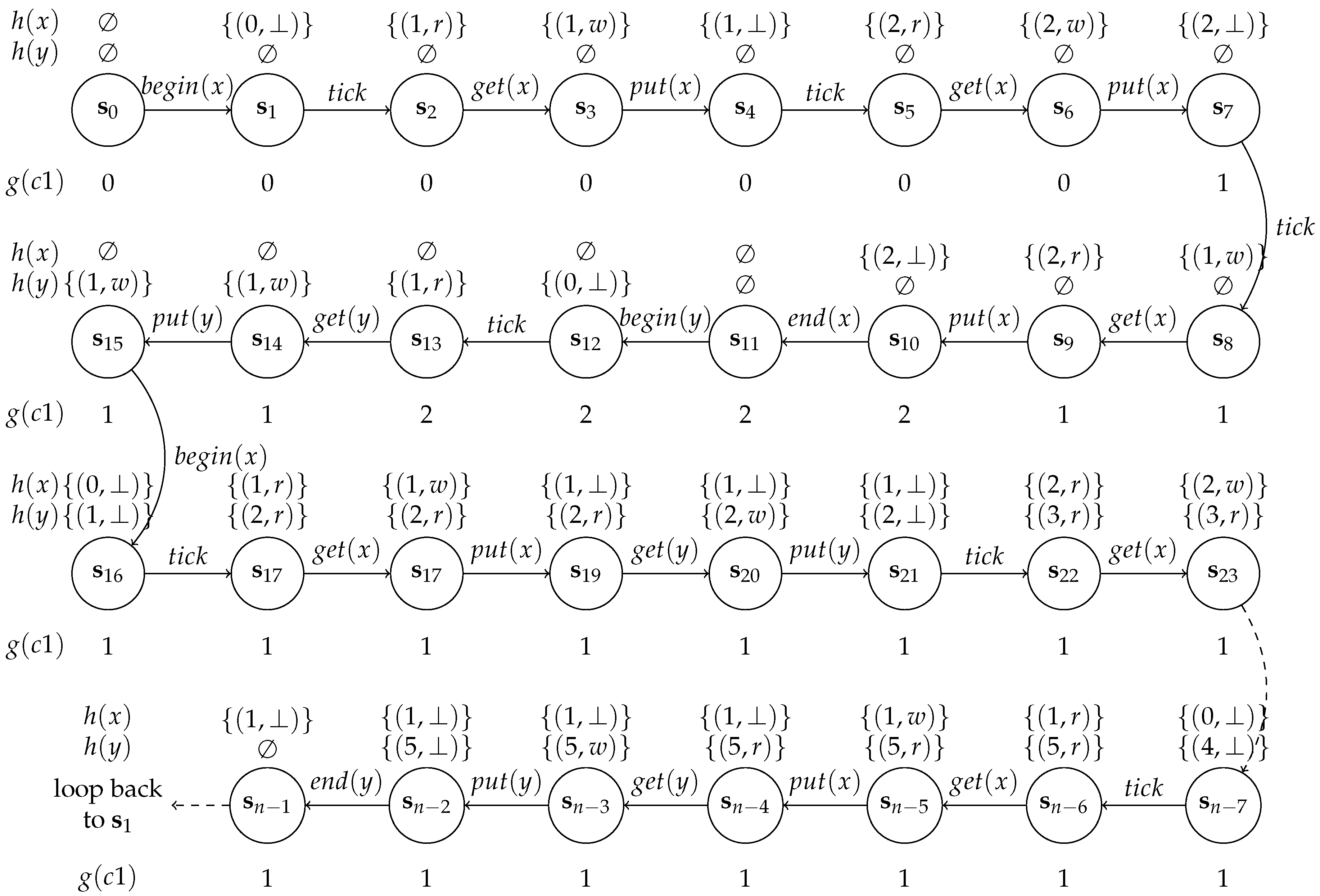
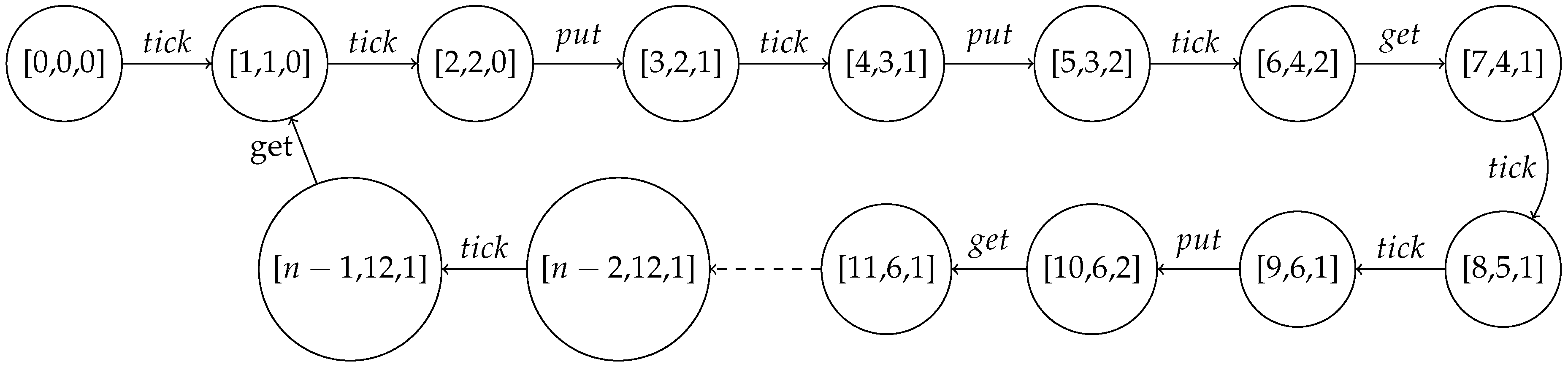
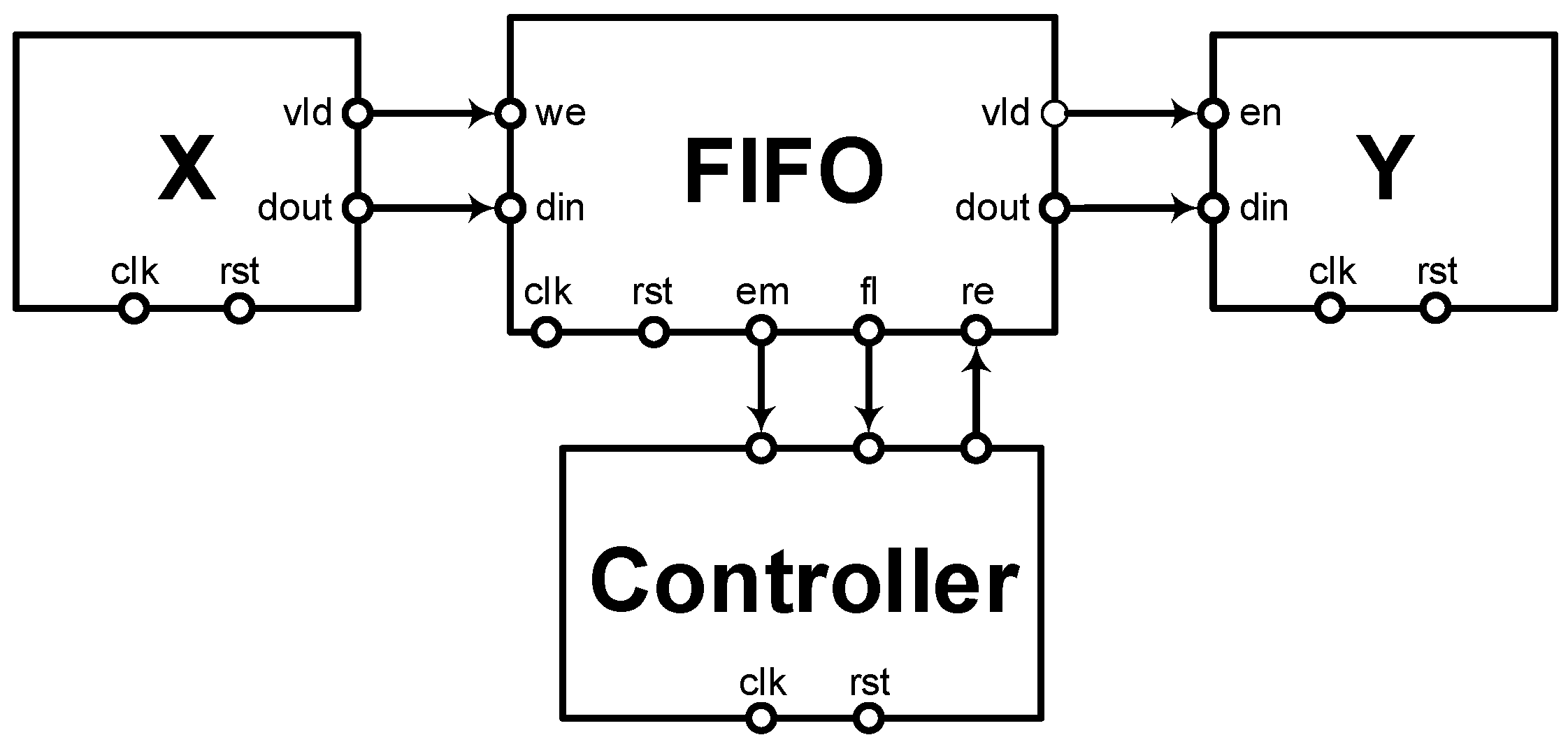
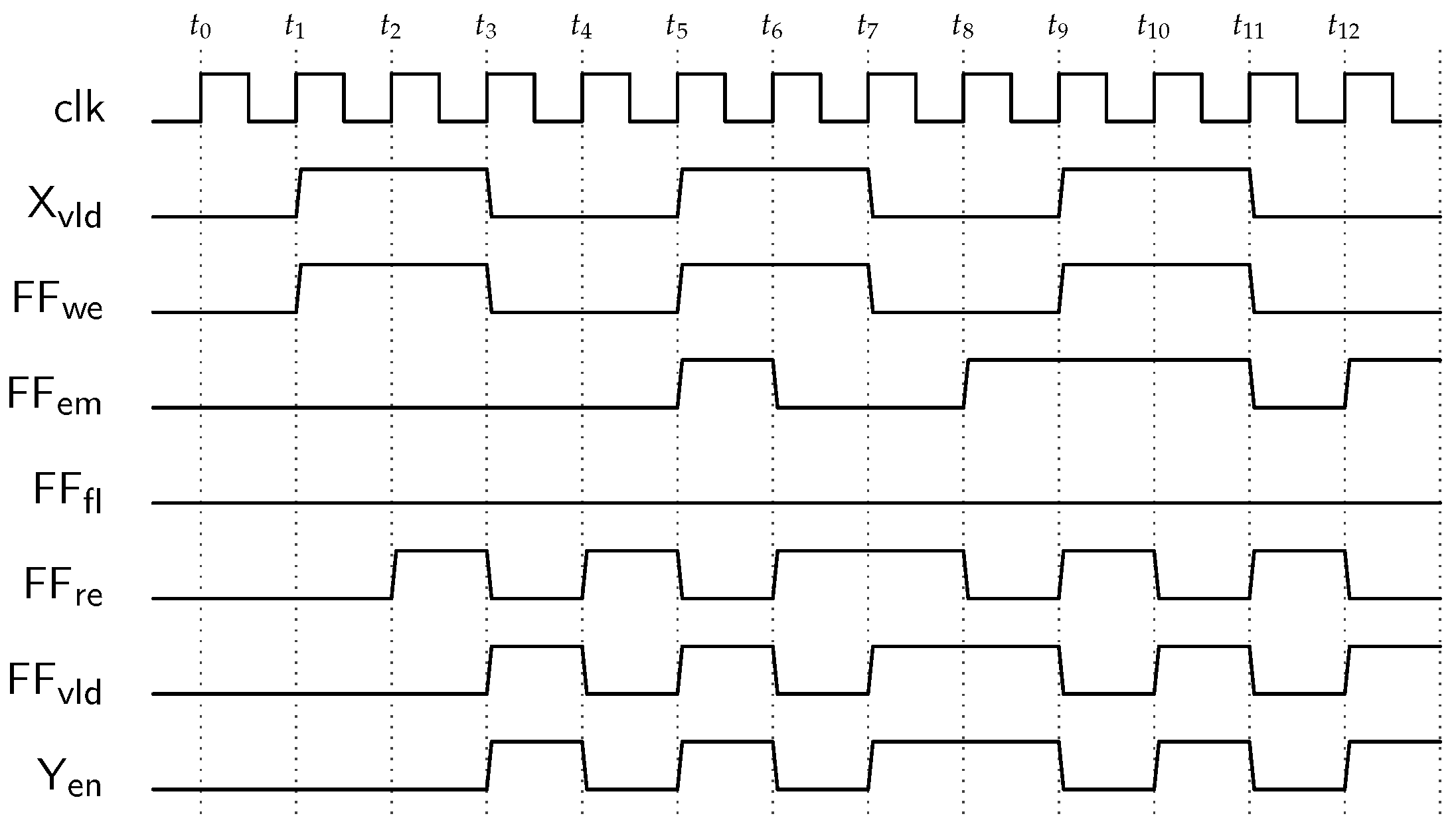
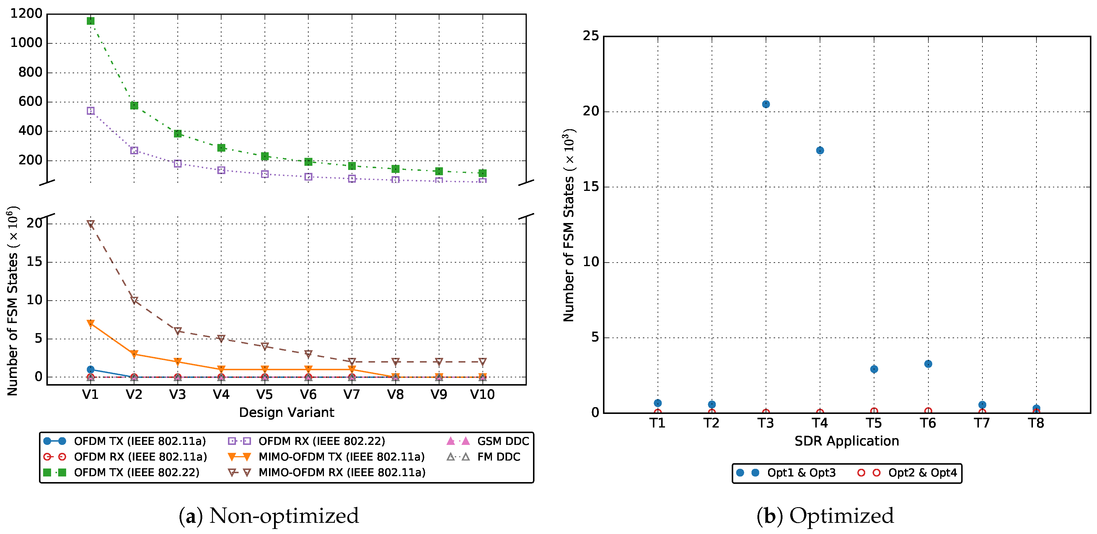
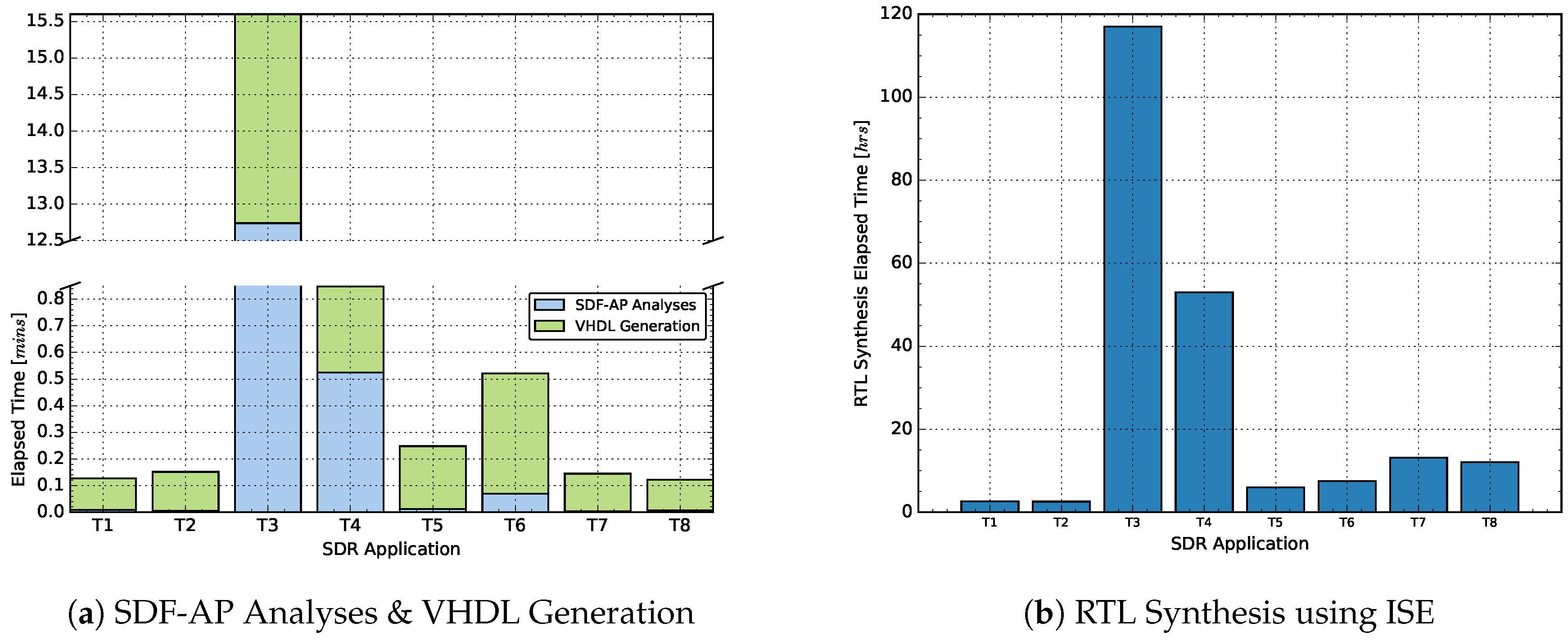
Table 1.
Types of states used for iterative optimization.
| State Type | Time Delay | Multiplicity | Has Transition Loop? | Condition for Next State Transition |
|---|---|---|---|---|
| s | [1..*] | Yes | ||
| s | [0..*] | Yes | ||
| s | 1..1 | No | or | |
| s | [0..*] | Yes | ||
| s | [0..*] | Yes |
Table 2.
The execution properties of different SDR applications.
| Application | Number of Actors | Number of FIFO Channels | Number of FIFO Channels with Buffer Size = 1 |
|---|---|---|---|
| OFDM TX (IEEE 802.11a) | 6 | 15 | 7 |
| OFDM RX (IEEE 802.11a) | 6 | 15 | 5 |
| OFDM TX (IEEE 802.22) | 6 | 15 | 7 |
| OFDM RX (IEEE 802.22) | 6 | 15 | 5 |
| MIMO-OFDM TX (IEEE 802.11a) | 22 | 59 | 28 |
| MIMO-OFDM RX (IEEE 802.11a) | 22 | 59 | 16 |
| GSM DDC | 11 | 23 | 10 |
| FM DDC | 13 | 27 | 10 |
Table 3.
The throughput constraints for SDR applications.
| Application | All | Design Variants | |||||||||
|---|---|---|---|---|---|---|---|---|---|---|---|
| V1 | V2 | V3 | V4 | V5 | V6 | V7 | V8 | V9 | V10 | ||
| OFDM TX (IEEE 802.11a) | T1 | 0.000775 (10%) | 0.001550 (20%) | 0.0023260 (30%) | 0.003101 (40%) | 0.003876 (50%) | 0.004651 (60%) | 0.005426 (70%) | 0.006202 (80%) | 0.006977 (90%) | 0.007752 (100%) |
| OFDM RX (IEEE 802.11a) | T2 | 0.000781 (10%) | 0.001563 (20%) | 0.002344 (30%) | 0.003125 (40%) | 0.003906 (50%) | 0.004688 (60%) | 0.005469 (70%) | 0.006250 (80%) | 0.007031 (90%) | 0.007813 (100%) |
| OFDM TX (IEEE 802.22) | T3 | 0.000024 (10%) | 0.000049 (20%) | 0.000073 (30%) | 0.000098 (40%) | 0.000122 (50%) | 0.000146 (60%) | 0.000171 (70%) | 0.000195 (80%) | 0.000220 (90%) | 0.000244 (100%) |
| OFDM RX (IEEE 802.22) | T4 | 0.000024 (10%) | 0.000049 (20%) | 0.000073 (30%) | 0.000098 (40%) | 0.000122 (50%) | 0.000146 (60%) | 0.000171 (70%) | 0.000195 (80%) | 0.000220 (90%) | 0.000244 (100%) |
| MIMO-OFDM TX (IEEE 802.11a) | T5 | 0.000417 (10%) | 0.000833 (20%) | 0.001250 (30%) | 0.001667 (40%) | 0.002083 (50%) | 0.002500 (60%) | 0.002917 (70%) | 0.003333 (80%) | 0.003750 (90%) | 0.004167 (100%) |
| MIMO-OFDM RX (IEEE 802.11a) | T6 | 0.000417 (10%) | 0.000833 (20%) | 0.001250 (30%) | 0.001667 (40%) | 0.002083 (50%) | 0.002500 (60%) | 0.002917 (70%) | 0.003333 (80%) | 0.003750 (90%) | 0.004167 (100%) |
| GSM DDC | T7 | 0.000391 (10%) | 0.000781 (20%) | 0.001172 (30%) | 0.001563 (40%) | 0.001953 (50%) | 0.002344 (60%) | 0.002734 (70%) | 0.003125 (80%) | 0.003516 (90%) | 0.003906 (100%) |
| FM DDC | T8 | 0.000781 (10%) | 0.001563 (20%) | 0.002344 (30%) | 0.003125 (40%) | 0.003906 (50%) | 0.004688 (60%) | 0.005469 (70%) | 0.006250 (80%) | 0.007031 (90%) | 0.007812 (100%) |
Table 4.
Comparison of features for different SDR prototyping tools.
| Features | Matlab + | Vivado | LabView | Frame-Based | Our |
|---|---|---|---|---|---|
| Simulink | HLS | DSL [28] | Framework | ||
| Domain-Specific to SDR | ✗ | ✗ | ✗ | ✓ | ✓ |
| Uses a dataflow-model of computation | ✗ | ✗ | ✓ | ✓ | ✓ |
| Dataflow supports access patterns | ✗ | ✗ | ✓ | ✗ | ✓ |
| Low-level hardware conformance to high-level design constraints | ✗ | ✗ | ✗ | ✗ | ✓ |
| Supports design re-use | ✓ | ✓ | ✓ | ✗ | ✓ |
| Automates optimizations | ✓ | ✓ | ✗ | ✓ | ✓ |
| Open-source and available to public | ✗ | ✗ | ✗ | ✓ | ✓ |
© 2018 by the authors. Licensee MDPI, Basel, Switzerland. This article is an open access article distributed under the terms and conditions of the Creative Commons Attribution (CC BY) license (http://creativecommons.org/licenses/by/4.0/).
Share and Cite
MDPI and ACS Style
Tsoeunyane, L.; Winberg, S.; Inggs, M. Automatic Configurable Hardware Code Generation for Software-Defined Radios. Computers 2018, 7, 53. https://0-doi-org.brum.beds.ac.uk/10.3390/computers7040053
AMA Style
Tsoeunyane L, Winberg S, Inggs M. Automatic Configurable Hardware Code Generation for Software-Defined Radios. Computers. 2018; 7(4):53. https://0-doi-org.brum.beds.ac.uk/10.3390/computers7040053
Chicago/Turabian StyleTsoeunyane, Lekhobola, Simon Winberg, and Michael Inggs. 2018. "Automatic Configurable Hardware Code Generation for Software-Defined Radios" Computers 7, no. 4: 53. https://0-doi-org.brum.beds.ac.uk/10.3390/computers7040053
Note that from the first issue of 2016, this journal uses article numbers instead of page numbers. See further details here.