1. Introduction
InN, as one of the members in the III-nitrides group, has attracted intensive interest ever since being discovered with a narrow band gap (e.g., ~0.7 eV) by Davydov et al. [
1] and is predicted to have the highest electron mobility among the III-nitrides group (~4400 cm
2/V∙s). These characteristics mentioned above make InN a potential material in high-speed electronic device (HEMT), photodetectors, solar cells and light-emitting devices [
2,
3,
4,
5]. However, practical application is still limited by the large number of defects, which is caused from dislocations, native and extrinsic defects such as threading dislocations, V
N, Si, O and H [
6,
7]. Moreover, Fermi-level pinning above the conduction band accompanied with donor-like surface state led to an ultrahigh-density of the surface electron accumulation layer. Most InN samples reported are degenerate n-type materials with an electron concentration of about 1 × 10
18 cm
−3 or even higher. In order to understand the fundamental properties of InN, much research has been conducted, especially on the photoluminescent (PL) properties of InN, which has been investigated intensively [
8,
9,
10,
11]. In semiconductor materials, the optical properties are extremely sensitive to carrier concentration, i.e., blueshift of peak energy and the broadening of full-with-half-maximum (FWHM) with increasing carrier concentration. Recently, many groups have discussed the high emission energy luminescence above the theoretical bandgap value in degenerate InN samples [
11,
12]. Such high energy peaks have been attributed to Mahan excitons (the recombination between electrons near the Fermi level and localized holes) and examined by photoluminescence spectra and reflectivity measurements [
12].
This study shows the optical properties and carrier dynamics of degenerate InN samples with different carrier concentrations (higher than 1 × 1018 cm−3) in photoluminescence and time-resolved photoluminescence spectra. The high energy transition, appearing above the conventional bandgap value of 0.7 eV, was explained by Mahan excitons. The evidence of Mahan excitons was further examined by time-resolved photoluminescence spectra, which reveal strong localization phenomena near the photon energy of the Mahan excitons within the degenerate samples.
2. Results
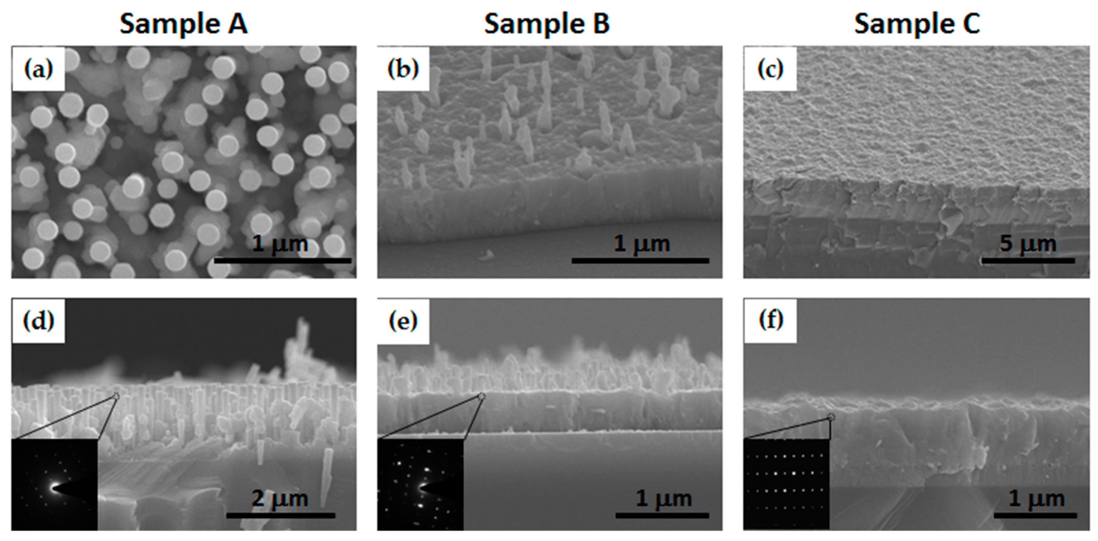
Figure 1 shows the SEM images of the InN samples with different growth temperatures (T
g). The surface morphology of InN transferred from nanorods (sample A) to thin films (sample C) with increasing T
g. In our experiments, the InN nanorods tend to form at lower growth temperatures, while the two-dimensional layers are formed at higher temperatures. In addition, no metallic droplet was observed at the end of the nanostructured InN, and this is strong evidence that the nanorods are grown via the self-catalyst process. The enhanced 2D growth mode is related to higher growth temperatures. This observation might be contributed to the enhancement of the InN atoms’ surface mobility with increasing temperature. In addition, the enhanced surface atomic mobility could cause a greater proportion of indium atoms to diffuse to reach the (0001) surface, which may provide more energetically stable binding sites. It is expected that the higher growth temperature of InN may result in a higher decomposition rate due to the thermal decomposition or thermal etching of the grown InN. Consequently, the InN samples grown at lower temperature results in an enhanced 1D characteristic. The self-catalyzed rod length and the diameter in sample A are approximately 1.3 μm and 150 nm, respectively. As T
g increased to 495 °C, the surface became rougher, accompanied by the coexistence of the rod and film structure. The thickness of the film was approximately 500 nm as shown in sample B. At the highest T
g of 525 °C, sample C revealed an obvious two-dimensional film growth pattern. These observations indicated that the growth temperature plays an important role in the morphology revolution of InN samples. In addition, the selected area electron-diffraction (SAED) pattern clearly demonstrates that both the InN nanocolumns and film have good crystallization quality.
Table 1 presents a detailed profile of different samples with various growth temperatures. These results show that, as T
g increased, carrier concentrations (n
Hall) first increased from 2.5 × 10
19 cm
−3 (sample A) to 1.63 × 10
20 cm
−3 (sample B) and then decreased to 1.14 × 10
20 cm
−3 (sample C). This phenomenon might be attributed to different surface mobilities between indium and nitrogen atoms under various growth temperatures. Hence self-catalyzed InN nanorods formed homogeneously in sample A with the lowest carrier concentration. As T
g increased, the difference in surface mobility became larger, resulting in the coexistence of the rod and film in sample B. This difference could also create more point defects. According to the first principle calculation [
7], donor-like nitrogen vacancy (V
N) has the lowest formation energy in the n-type InN samples and the formation of V
N leads to high carrier concentrations. At the highest T
g, both indium and nitrogen atoms have enough lateral migration to form thicker film homogeneously at a lower carrier concentration.
Figure 2 shows the low-temperature PL spectra of all samples, indicating that the samples have a dominant peak with one (sample A) or two (sample B, C) low energy side peaks and a high energy shoulder. The emission spectrum broadened with a higher Hall concentration, which can be attributed to the band filling effect. The transition energy for the peaks was similar in the low energy range below 760 meV. However, for high concentration samples (samples B and C), higher energy peaks appeared with high energy shoulders simultaneously moving toward the higher energy side. The emission energy for the samples was complex and far above the commonly accepted band gap value of InN (0.65–0.7 eV). Peaks with a transition energy higher than the band gap are typically attributed to the degenerate electrons-to-band or to-acceptor level [
8]. However, high energy peaks for these samples had more intensive luminescence than the low-energy peaks. This is less likely to be explained by degenerate-to-band due to the small amount of high k-value holes in the valance band of n-InN. Hence, the high energy peaks in this case could arise from degenerate electrons-to-acceptors. Moreover, these peaks had more intensive emissions. Recently, the high emission energy and high intensity of luminescence were explained by the Mahan excitons [
13]. The Mahan excitons can be described as widely k-spread localized holes interacting with all electrons in the conduction band as the electrons locate at Fermi edge. The optical transition matrix is strongly enhanced because of the enhanced carrier scattering, whereas the electrons below the Fermi level have only a weak recombination with localized holes. Thus, the high emission energy peaks in degenerate semiconductors are more intensive than those near band edge one.
To confirm the recombination mechanism, a low temperature luminescence line shape was fitted by Equation (1) and multi-Gauss function:
In Equation (1),
is the photon energy,
is the band gap value,
represents the energy of acceptor state above the valance band,
is the quasi-Fermi energy and
and T are the Boltzman coefficient and the electron temperature, respectively. The adding of the Gaussian band interprets the enhancement of the optical matrix of the Mahan excitons [
14].
Table 2 lists a summary of the fitting results. For example, the average energy spacing between P1 and P2 was 48 meV. These values are in line with the difference of binding energy of deep (50–85 meV) and shallow (5–10 meV) acceptors [
8]. Furthermore, the energy of P2 had an average value of 6 meV lower than the fitted band gap, which corresponds well with the binding energy of shallow acceptor. Hence, we assigned P2 as the complex of the band-to-shallow acceptor and the band-to-band recombination, and P1 resulted from the band-to-deep acceptor. Samples B and C had a concentration in the order of ~10
20 cm
−3. Therefore, the main peaks were far above the fitted band gap and had an average value of 66 meV lower than the Fermi energy. This confirmed the main peaks in samples B and C were the result of the degenerate-to-deep acceptors of the Mahan excitons.
Energy-dependent TRPL (ED-TRPL) was conducted to further confirm the Mahan excitons in these samples. The deep localized holes involved in Mahan excitons can trap carriers, preventing them from escaping from localization and leading to a long lifetime. The ED-TRPL of samples in
Figure 3 show results that support the existence of localized states, where the lifetime was fitted by single-exponential decay as Equation (2):
In Equation (2), represents luminescence intensity at = 0 and is the characteristic time of decay curve or simply carrier lifetime. Because of the instrument limitations, the minimum energy level we could analyze was approximately 730 meV. This energy is unsuitable for lower emission energy but is enough to observe the most peaks in the samples. The fitted lifetime shows that the longest lifetime was perfectly matched to the dominated peaks for samples B and C, which indicates the strongest localization in the assumed Mahan excitons recombination peaks.
Except for the main peaks, ED-TRPL data exhibit shoulder near the second strongest peak for sample B and C. This slight standstill of lifetime at the shoulders also indicated a localization phenomenon but was weaker than the main peak because of the shorter carrier lifetime. However, the longest lifetime in sample A was located at energy higher than the main peak of sample A, which was assigned as near band edge recombination. In samples B and C, the carrier dynamics are mainly dominated by thin film characteristics. On the other hand, the longest lifetime in sample A was located at energy higher than the main peak of sample A, which was assigned as near band edge recombination. This result might be because of the absence of Mahan excitons in the nanorod structure. The reason for this phenomenon is still unclear and will be further discussed in the future.
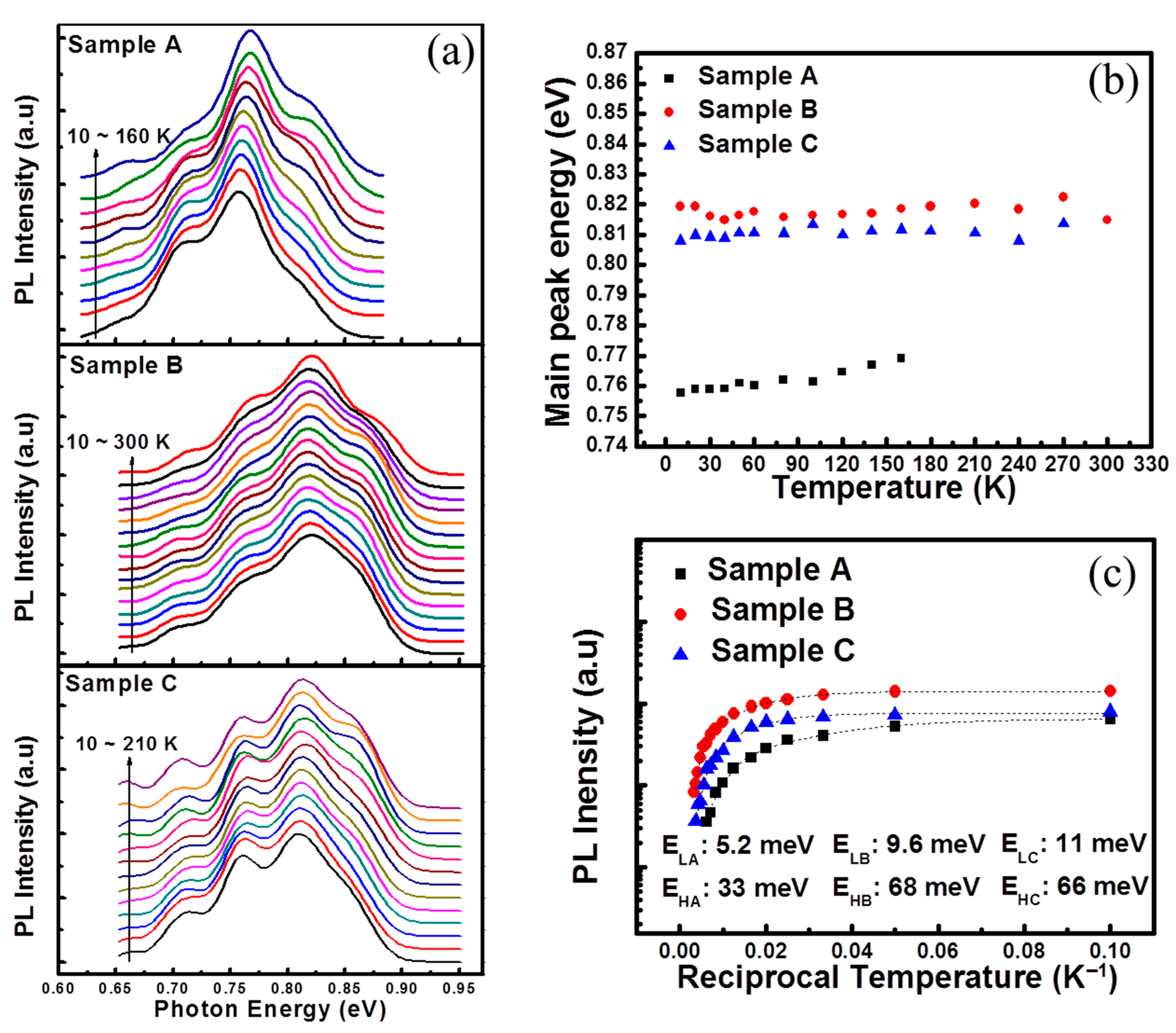
Figure 4a shows the temperature-dependent PL spectra taken from three samples with various morphologies
. For the nanorod structure in sample A, the main peak (near-band-edge recombination) shows significant blue shift in
Figure 4b at all temperature ranges. However, the PL signal of sample A decreased more rapidly than the film type samples of samples B and C. In addition, its spectrum cannot be analyzed with temperatures over 160 K. The blue shift of the main peak in sample A can be attributed to the band-bending near the rod’s surface, as induced by the intrinsic electron accumulation layer. The large surface-to-column ratio of the rod structure can lead to a more significant band-bending phenomenon than the thin film structure. The photoholes tend to move from low energy state at the rod center to high energy states near the surface as the temperature increased, leading to an anomalous blue shift [
15]. The rapid decrease of luminescence intensity in sample A can be also attributed to the large surface-to-column ratio, which makes the influence of surface state more significant. On the contrary, samples B and C show strong luminescence even at high temperatures. Meanwhile, the peaks positions in
Figure 4b show no clear shift over all temperature ranges. In this case, samples B and C had higher carrier concentrations than sample A. In such highly degenerate semiconductors, band gap shrinkage induced by temperature can be easily compensated for by an increased electron Fermi level (E
Fn), hence leading to nearly no shift of peaks [
11]. The Arrhenius plot of the main peak of samples appears in
Figure 4c. The PL intensity decreased monotonically with the temperature because of the activation of the nonradiative recombination center. To extract the activation energy, Equation (3) was conducted to fit the experiment data in
Figure 4c:
In Equation (3),
represents the 0 K PL intensity,
and
are the thermal quenching coefficients and
and
are the activation energy at low and high temperature, respectively. The dash lines in
Figure 4c shows the fitting result, which match well with the experimental data. The fitted low- and high-temperature activation energies appear in this figure. These results show that the high-temperature activation energies of samples B (68 meV) and C (66 meV) matched the deep acceptor levels of InN material. The high-temperature activation energy of sample A showed a large discrepancy with other samples. This smaller value indicates a stronger thermal quenching effect, which can be ascribed to the large number of surface states for the nanorod sample.
3. Materials and Methods
InN samples were grown by home-made chemical-beam epitaxy (CBE, TIRI, Hsinchu, Taiwan) on c-plane sapphire substrate with a GaN buffer layer. The GaN buffer layer was pre-grown by metal-organic chemical vapor deposition (MOCVD, Aixtron, Herzogenrath, Germany) system before the growth of InN. The group III and N source was trimethylindium (TMIn) and an RF plasma-induced nitrogen atom, respectively. In this work, we fixed the V/III ratio at 1, and the growth temperature (Tg) was 465 °C, 495 °C and 525 °C (denoted as sample A, B and C). After the InN samples were prepared, the carrier concentration was carried out by standard Hall measurement system using the van der Pauw configuration with a 0.32 T magnetic field at room temperature. For Hall tests on all InN samples, In pellets are used as ohmic metal contacts and the pellets are 99.99% pure with a ball diameter of about 1 mm. Conventional transmission electron microscopy (TEM, JEOL, Tokyo, Japan) and X-ray diffraction (XRD, Jordan Valley Semiconductor, Hsinchu, Taiwan) have been used to study the crystalline structure of the samples. The optical property was performed by photoluminescence (PL) and time-resolved photoluminescence (TRPL) in a close-cycle helium cryostat chamber equipped with a temperature controller. The excitation source is a 635 nm line semiconductor laser for both the PL and TRPL measurements, which can be switched between CW and pulsed mode. The repetition rate for the TRPL measurement is 80 MHz and the laser pulsed width is 76 ps. The PL and TRPL signals were dispersed by a 0.5 m monochromator (Horiba, Taipei, Taiwan) using 600 groove/mm grating and detected by a current-cooling InGaAs photodiode (working range: 900 nm–2100 nm) and an infrared photomultiplier tube (Horiba, Taipei, Taiwan) (working range 1000 nm–1700 nm), respectively.


 ,
, 


