1. Introduction
During the last decade, a clearly pronounced trend in the field of heterogeneous photocatalysis is the deliberate construction of novel photocatalytic systems based on the semiconductor heterostructures, which are able to absorb solar light and convert its energy into redox chemical reactions [
1,
2].
By the term “heterostructure”, we mean an integration of two or more semiconductors into an indivisible light absorbing system with interphase boundaries (heterojunctions), and the semiconductor components interacting by means of energy/charge transfer. As expected, the heterostructures can promote (i) an extension of the light absorption spectrum toward longer wavelengths, and consequently, a better utilization of incident solar irradiation; (ii) a minimization of energy losses when the system transforms to a state in which it becomes capable of participating in redox heterogeneous chemistry.
So far, major attention has been given to the creation and investigation of heterostructured photoactive materials of type II [
3] composed of two (or more) semiconductors with different band gaps and corresponding positions of the valence and conduction bands as presented in
Figure 1a. In general, type II heterostructures are able to absorb light in a wider spectral range; however, the redox ability of such systems (which in a simplified model is determined by the relative positions of the electron and hole energy levels at quasi-stationary states of the system under irradiation) is less than the redox ability of each individual component of the heterostructure. In other words, the type II heterostructure system is only capable of driving photochemical processes with |ΔG| smaller than each single semiconductor component of heterostructure in spite of the wide spectral range of photoactive light absorption. As a result, such systems could be inefficient in most desired photochemical redox processes, such as water decomposition or CO
2 reduction to produce “solar fuel” [
4].
In 2013, J. Yu and coauthors reported the results of an experimental demonstration of direct Z-scheme performance in photocatalytic process [
5]. Since then, a rapid growth of studies directed toward the realization of direct solid-state Z-scheme (see
Figure 1b) has been observed [
6].
Should the direct Z-scheme be truly created, the reduction potential of such heterostructure systems under irradiation would correspond to the energy of the bottom of the conduction band of the SC1 component and the oxidation potential of heterostructure would relate to the energy of the top of the valence band of the SC2 component. Therefore, the difference of redox potentials becomes significantly larger than the redox potentials of each component of the heterostructures and therefore, such heterostructures are able to drive photochemical processes with large |∆G|. At the same time, the spectral range of photoactivity of Z-scheme heterostructures is also extended (similar to type II heterostructures) and light energy absorbed by both components of the heterostructure is used to initiate and to drive redox reactions.
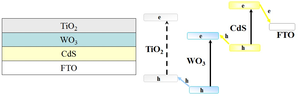
N. Serpone and A.V. Emeline [
7] have proposed a three-component nanostructure. According to the proposed scheme, two narrow-band semiconductors absorb light energy and transfer it in electronic form to a wide-band semiconductor, which initiates a consequent redox reaction. In addition, the wide-band gap semiconductor covering the narrow band gap components protects them from corrosion and decomposition in the photochemical side reactions. Therefore, a ternary heterostructure system should demonstrate all the advantages of the direct all-solid Z-scheme in terms of the expanded spectral range of photoexcitation and redox ability together with higher photochemical stability. To create such a ternary heterostructure system, three semiconductors with different band gaps, CdS, WO
3, and TiO
2, can be used (see
Figure 2).
As emphasized by other authors, photocatalytic tests imply that the construction of multiple component heterostructures favors achieving an efficient separation of photo-generated electrons and holes. For instance, H. Zhang and coauthors recently demonstrated [
8] that the Bi
2MoO
6/WO
3/Ag
3PO
4 heterostructure’s photocatalytic performance exceeded the photoactivity of its single components, pristine Ag
3PO
4, WO
3/Ag
3PO
4 and Bi
2MoO
6/Ag
3PO
4, by 3.16 times, 2.63 times, and 1.75 times, respectively.
The two-component TiO
2/CdS heterostructure has been under investigation for a long time [
9], first as a sensitized TiO
2 system. This system continuously attracts attention due to relative simplicity of its formation and promising potential for solar fuel production, together with other valuable products [
10,
11]. Nowadays, some researchers report that the direct Z-scheme heterojunction can be easily realized in this system. For instance, J. Low et al. have provided strong evidence based on ISI-XPS characterization, hydroxyl radical generation test, and DFT simulation, that confirms the formation of the direct Z-scheme heterojunction between TiO
2 and CdS [
12].
The TiO
2/WO
3 heterostructured system, used as photocatalyst, has been also highlighted in numerous publications [
13]. The reported results of photocatalytic behavior of such a heterostructure are very promising. S. Prabhu et al. [
14] claim that the TiO
2/WO
3 heterostructures show 17 times higher photon-to-hydrogen conversion efficiency than pure TiO
2 and WO
3 under solar light and almost complete removal of organic pollutants in 60 min under visible light.
TiO
2/CdS/WO
3 ternary heterostructure was also recently studied [
15]. CdS and WO
3 were used in the form of hierarchical WO
3-nanosheet/CdS-nanorod arrays to produce a heterostructure, and TiO
2 was used as a protection layer. This type II heterojunction photoanode demonstrated a photocurrent density of 5.4 mA cm
−2 at 0.8 V versus a reversible hydrogen electrode for sulfite oxidation that is 12 times greater than that of WO
3-nanosheet array (0.45 mA cm
−2) and 3 times higher than CdS-nanorod arrays (1.85 mA cm
−2). The authors suppose that the favorable heterojunction between WO
3 and CdS enhances the charge separation efficiency and widens the light absorption spectrum.
In this study, we performed a comparative exploration of photoelectrochemical behavior of the binary CdS/TiO2 and WO3/TiO2 and ternary CdS/WO3/TiO2 heterostructures based on titania nanotube and planar structures. Particularly, we demonstrated the possibility for the realization of Z-scheme of photoexcitation and charge separation in planar heterostructured systems.
2. Results
As evident from the presented data, both nanotube-based and planar TiO2 electrodes demonstrate a significant hysteresis typical for TiO2 both in the dark and under irradiation, originating from the charging-discharging intrinsic defect states at the surface and in the near-surface spatial region of TiO2. However, the hysteresis is significantly changed and diminished in the case of formation of binary and ternary heterostructures. This indicates, on the one hand, a successful formation of heterojunctions between semiconductors and on the other hand, an appearance of new charge transfer pathways that play a dominant role in the heterostructures. In other words, formation of heterostructures significantly screens the effects of defect states becoming a major factor in photoelectrochemical processes. For further discussion, it is wise to note the similarity of the curves obtained for binary CdS/TiO2 and ternary CdS/WO3/TiO2 nanotube-based heterostructures, which suggests that CdS plays a significant role in both heterostructures.
Formation of binary and ternary heterostructures is also confirmed by the results of electrochemical impedance spectroscopy (EIS). It is commonly known that EIS analysis provides information about the interfacial properties of electrodes [
16].
Figure 4 demonstrates the EIS dependencies obtained for both nanotube (
Figure 4a) and planar (
Figure 4b) electrodes under irradiation. Corresponding dependencies measured in the dark are presented in
Figure S2 (Supplementary Materials).
These dependencies can be presented in the form of the EIS Nyquist plots (see
Figures S3 and S4 in Supplementary Materials). The curvature of the semicircle in EIS Nyquist plot is related to the electron transfer resistance, which reveals electron transfer kinetics of the redox pair at the electrode/electrolyte interface. As indicated in the
Section 5, the character of behavior of the electrodes in the dark and under the irradiation can be simulated by the equivalent circuit scheme presented in
Figure 5.
Calculated values of the active resistances and parameters of CPE are given in
Table 1 for nanotube-based systems and in
Table 2 for planar heterostructures, respectively (corresponding parameters measured in the dark are given in the
Tables S1 and S2).
A comparative analysis of the equivalent circuit scheme parameters, measured in the dark and under irradiation, shows that in the dark, the impedances of CPE in both nanotube-based and planar heterosystems demonstrate a capacitor behavior (n→1) with essentially large resistance R2 as is typical for heterostructures due to barrier formation at the heterojunctions. However, under irradiation, the impact of the capacitor behavior is significantly reduced (n << 1) as well as both active and reactive resistances also decrease (R2 and P). This indicates that photoexcitation of the heterosystems results in the generation of free charge carriers in all semiconductor components of the heterostructures, which in turn, decreases the barriers in the corresponding heterojunctions. Thus, photoexcitation opens pathways for effective electron transfer through the heterostructures.
From the presented data, one can conclude that in the set of nanotube electrodes, the resistance increases as WO3/TiO2 >> TiO2 ≈ CdS/TiO2 ≥ CdS/WO3/TiO2 while other characteristics remain nearly the same. It implies that WO3 in contact with Ti support creates an extra Ohmic resistance while for all other nanotube systems, a major contribution to resistance belongs to the titania nanotubes. At the same time, for the planar electrodes, the resistance changes as CdS/TiO2 ≥ WO3/TiO2 ≥ CdS/WO3/TiO2 >> TiO2 since the formation of planar heterojunctions increases the resistance of the electrodes. However, the ternary system demonstrates the minimal resistance comparing to binary systems.
Bode plots show a clear difference between nanotube and planar systems. It is evident that the planar systems’ behavior describes (at least) two different processes reflected by the presence of two phase shift extrema while nanotube systems demonstrate clearly only a single extremum. This difference can be assumed to be due to the difference in geometric structure between two types of heterostructures. Indeed, a large part of nanotube-based heterostructures consists of titania nanotubes and heterojunctions play a minor role in the system, while in planar heterosystems, a key-role in the photoelectrochemical behavior belongs to the heterojunctions between semiconductors. At the frequency where a maximum Z″ (ω) is observed, the straightforward relationship 1/ω
max = 1/(2π
fmax) = τ, where τ is a time constant of the electrochemical reaction, indicates the time scale of an electrochemical reaction [
17]. Accordingly, a certain time constant can be ascribed to each extremum (see
Table 3 and
Table 4 for nanotube-based and planar heterostructures under irradiation, respectively).
Comparing the values τ obtained for nanotube-based and planar heterostructures, one may conclude that this characteristic time parameter is much shorter for planar systems compared to nanotube based ones. This difference can be attributed to geometry (thickness) of the corresponding electrodes since nanotube-based structures are much thicker. Photoexcitation of the heterostructure electrodes results in significant decay of τ, regardless of the geometry of the electrodes.
It is also wise to note that the maximal values of τ are observed for the ternary heterostructure systems, both nanotube-based and planar, since the complex character of heterojunctions in such systems makes a pathway for charge carriers significantly “longer” compared to simpler structures.
Figure 7 demonstrates the transient kinetics of photocurrent behavior for both nanotube and planar electrodes when light irradiation is switched on.
The transient photocurrent decay is observed immediately after the illumination start (see
Figure 7), approaching to the stationary photocurrent for both nanotube and planar heterostructured electrodes. It is assumed that the photocurrent decays due to an enhancement of photogenerated electron-hole recombination and approaches a quasi-steady state value when the rates of electron-hole photogeneration and recombination become equal. Note, that the samples of ternary composition (both planar and nanotubes) show the highest initial photocurrent values and the slowest approach to the steady state. The transient time constant (
τdec) calculated by Equation (1), can be a characteristic of the efficiency of the system transition to quasi steady state behavior:
where
D is the transient photocurrent decay:
where
It is the photocurrent generated at time t,
Is is the steady state photocurrent, and
Ii is the initial photocurrent.
Calculated values of
τdec for both nanotube-based and planar systems are presented in
Table 5.
One can note that in the case of nanotube-based structures, the values τdec for CdS/TiO2 and TiO2 systems are about the same. Similar values τdec are also obtained for WO3/TiO2 and CdS/WO3/TiO2 systems. Therefore, the difference in τdec for these two groups can be attributed to the contact with higher resistance between WO3 and Ti substrate, and in the absence of WO3, the contact with the substrate is formed by TiO2 nanotubes only. Again, these results confirm the conclusions made from EIS data analysis that the major role in all nanotube-based systems is played by the titania nanotubes, while the heterojunctions have a minor effect on electronic processes in such electrodes. At the same time, the τdec values determined for planar samples are significantly different, which is most likely dictated by the difference in semiconductor heterojunctions formed in different planar heterostructures.
Spectral dependencies of incident photon-to-current conversion efficiency, IPCE, measured for both nanotube-based and planar heterostructures, are shown in
Figure 8.
As evident from the presented spectral dependencies in the spectral region of fundamental absorption of TiO2 (and therefore, of all components of the heterostructures), the highest IPCE is observed for ternary heterostructures regardless of their geometry (planar vs. nanotube). At the same time, there is a significant difference in the way the binary heterosystems affect the IPCE in the UV-spectral region depending on whether they are planar or nanotube based: For nanotube systems, the IPCE for binary systems (both WO3/TiO2 and CdS/TiO2) is higher than for TiO2 nanotubes, while for planar heterosystems, the IPCE registered for binary systems are lower than for pristine TiO2 electrode in accordance with the increase of resistance.
A remarkable difference for ternary heterosystems with respect to their geometry is observed in the visible spectral range: No significant photoactivity is detected for nanotube based heterosystems, while an essential photoresponse is observed for planar heterostructure electrode within the spectral range of 400—450 nm. Therefore, planar ternary heterostructure systems demonstrate strong photoactivity in the visible spectral range compared to both pristine TiO2 and binary heterostructure electrodes. It is wise to emphasize that the spectral edge of photoactivity at 450 nm corresponds well to the band gap of WO3 (~2.75 eV). In other words, the ternary planar heterostructured system shows its activity when both narrow band gap semiconductors, WO3 and CdS, are photoexcited in the fundamental absorption spectral region. This behavior of IPCE spectral dependence confirms our conclusion inferred from LSV data, that formation of heterojunctions is a major factor which determines the efficiency of photoelectrochemical process and significantly reduces the possible role of defect states in semiconductors. Taking into consideration the geometry of the planar ternary system, one may conclude that its photoactivity under visible light irradiation is possible only in the case when Z-scheme scenario of photoexcitation and charge separation is realized.
3. Discussion
Before starting an analysis of experimental results yielding the possible mechanisms of electrochemical behavior of heterostructured systems, it is wise to recall the geometry of the formed electrodes.
Figure 9 represents an expected geometry of the formed ternary heterostructures.
As seen in
Figure 9, the nanotube-based heterostructure electrode is characterized by a rather random distribution of narrow band gap semiconductor components in titania nanotubes due to the methods applied for their synthesis and formation. Based on the data provided by electron microscopy, one may expect that a significant part of titania nanotubes remains undecorated with narrow band gap semiconductors. At the same time, statistically, some nanotubes can be modified with only one of the components of the ternary system, either with WO
3 or with CdS. Obviously, a probability that titania nanotubes form heterostructures with both WO
3 and CdS and heterojunction between these narrow band gap semiconductors is not high. Therefore, ternary nanotube-based heterostructure electrodes consist of unmodified titania nanotubes and stochastically random sets of different heterojunctions, such as WO
3/TiO
2 and CdS/TiO
2 only, a combination of both WO
3/TiO
2 and CdS/TiO
2, and CdS/WO
3/TiO
2 in different nanotubes. Accordingly, it creates a possibility for various electron transfer processes within nanotube-based electrodes as demonstrated in
Figure 10a.
On the other hand, one may expect a completely different scenario for the ternary planar system, whose geometric layer-by-layer structure is well ordered due to the approach applied for its formation. Accordingly, there is only a limited and specific set of electron transfer processes that may occur in such heterostructure electrodes, as demonstrated in
Figure 10b. Accordingly, photoexcitation in the visible spectral range can lead to electrochemical activity of the ternary planar system only if both WO
3 and CdS components are photoexcited. Otherwise, the heterojunction barriers would prevent charge carrier migration from the outer surface of TiO
2 layer to the contact layer at the FTO substrate. By contrast, in nanotube-based systems, the outer surface of TiO
2 is in direct contact with the Ti substrate through titania nanotubes. Therefore, the heterojunctions formed with narrow band gap semiconductors play a rather minor role in charge carrier migration. Summing up, we conclude that ternary planar systems demonstrate their photoactivity due to realization of Z-scheme of photoexcitation and charge separation.
4. Materials and Methods
4.1. Preparation of TiO2 Nanotubes and Binary (CdS/TiO2, WO3/TiO2) and Ternary (CdS/WO3/TiO2) Heterosturcture Systems
TiO2 nanotubes (TNT) were prepared by anodic oxidation of Ti-foil (99.99%) in ethylene glycol electrolyte containing ammonium fluoride (0.1 wt %) with deionized water (2 vol %). All anodization processes were performed in a conventional two-electrode electrochemical cell with titanium foil as an anode and platinum foil as a cathode at constant voltage (60.0 V) at room temperature for 2.5 h. After anodization was completed, the samples were washed with deionized water and dried at 100 °C followed by annealing at 500 °C for 2 h (heating/cooling rate of 30 °C/h) to transform amorphous TiO2 to crystalline phase.
The binary WO3/TiO2 heterostructure system was formed by electrochemical deposition of tungsten on the Ti foil by using sodium tungstate (1M) as a W precursor and a mixture of dimethylformamide and formamide (volume ratio 1/9) as an electrolyte. The electrochemical deposition was carried out for 1 h at potential −2.0 V. Thereafter, the substrate was washed with deionized water. Then, the obtained substrate was used as an anode for anodization process to form TiO2 nanotubes at the same conditions as reported above.
The electrochemical deposition of CdS was performed using the obtained TiO2 and WO3/TiO2 samples as working electrodes in an aqueous electrolyte containing 0.002 M CdSO4 and 0.1 M Na2S2O4 at pH = 7. An electrochemical reduction of bisulfate ions to sulfide ions followed by deposition in the form of CdS at TiO2 nanotubes surface, was performed at the potential −0.6 V for 30 min.
4.2. Preparation of TiO2 Films, and Binary (CdS/TiO2, WO3/TiO2) and Ternary (CdS/WO3/TiO2) Planar Heterosturcture Systems
All planar systems were deposited on FTO glass substrates, preliminarily washed in acetone for 30 min using ultrasound bath and dried at 200 °C.
The TiO2 polycrystal dense layer in all planar systems was formed by a sol-gel dip coating method (KSV Nima dip-coater). TiO2 sol was produced using 9 mL titanium isopropoxide, 100 mL isopropyl alcohol, and 18 g citric acid, which were thoroughly mixed and left to age for 24 h. The dense TiO2 film was formed by immersion into sol solution four consecutive times with withdrawing velocity of 10 mm min−1 and drying the deposited film for 30 min before next immersion. Then, films were annealed at 450 °C in air for 5 h to crystallize the film and to remove all residual organics.
CdS polycrystal layer was chemically formed on FTO glass support for both binary and ternary CdS-containing heterostructured systems by deposition from the aqueous solution prepared by mixing 0.1 M ammonia as a stabilizer, 0.002 M thiourea as a reducing agent, and 0.001 M CdSO4 as a precursor. The deposition was carried out in thermostatic conditions at 70 °C for 30 min. After film deposition, the electrodes were washed with deionized water and dried at 100 °C.
WO3 polycrystal layers were formed on either FTO glass or CdS/FTO substrates by the dip coating method. A WO3 sol solution was prepared from WO3 powder (2 wt %) dissolved in concentrated ammonia at 60 °C. An immersion was carried out consequently eight times with withdrawing velocity of 10 mm min−1 and drying at 200 °C for 15 min after each immersion. Then, samples were annealed at 450 °C at the air for 5 h.
As a result, the following layered samples, TiO2, WO3/TiO2, CdS/TiO2, CdS/WO3/TiO2, were formed on FTO glass substrates and the TiO2 layer was always on top of the planar heterostructured electrodes.
4.3. Material Characterization
X-ray diffraction method was used to analyze phase formation with Bruker “D8 DISCOVER” high-resolution diffractometer (CuK
α radiation) in the angle range of 20° ≤ 20° ≤ 80° at a scanning speed 5.0°/min. The data analysis by the Rietveld method was carried out using the TOPAS (Bruker AXS) software. According to XRD analysis, the produced samples, both nanotubes and planar, were crystallized in the phases corresponding to the desired components of heterostructures (TiO
2 anatase, CdS, WO
3 (monoclinic)) (see
Figure S6 in the Supplementary Materials).
The surface morphology was explored by scanning electron microscopy (Zeiss Supra 40 VP system) for all synthesized semiconductor electrodes (see
Figures S7 and S8). As evident from SEM images, the titanium dioxide nanotube layer was uniformly distributed on the substrate, the pores in the obtained layer were normally oriented to the substrate plate. The diameter of the tubes was about 70 nm and its thickness (nanotube length), about 1 µm. Electron microscopy images of planar systems confirm a successful deposition of the layers of each component of the heterostructures (see
Figure S8) and formation of the dense outer layer of TiO
2 reliably covering and protecting inner layers of the heterostructures.
To validate the presence of narrow band gap semiconductors in the titanium dioxide nanotubes, the XPS spectra of the heterostructure systems were examined. The spectra are presented in
Figure S9 (see Supplementary Materials). The peaks related to the binding energies ~458.4 eV and ~464.2 eV, correspond to Ti2p3/2 and Ti2p1/2, respectively. According to the reference data [
18], Ti
4+ is the dominant oxidation state of titanium ions in nanotubes. The peaks at binding energies of 35.5 eV, 405.1eV, and 168.5 eV in the XPS spectra of the ternary heterostructure system correspond to the W4f, Cd3d, and S2p states, respectively. The O1s peak at ~529.60 eV demonstrates a symmetric shape for both pristine titania nanotubes and ternary system. Thus, the O1s XPS spectra give no evidence of the presence of more than one type of oxygen state.
4.4. Photoelectrochemical Experiments
Photoelectrochemical measurements were performed at room temperature in a three-electrode cell with a quartz window. All potential measurements were performed against the Ag/AgCl reference electrode (0.222 V vs. potential of NHE). Platinum wire was used as a counter electrode. Na2SO4 (1M) aqueous solution was used as an electrolyte. A computer-controlled ZAHNER CIMPS-2 (ZAHNER-elektrik, GmbH & Co. KG, Germany) potentiostat was used for electrochemical measurements. The dependences of photocurrent on intensity and wavelength of acting light were carried out with the setup of CIMPS-LED light sources.
The incident photon-to-current conversion efficiency (IPCE) values were calculated using the following equation [
19]:
where 1239.8 (in V·nm) is a multiplication of Plank’s constant,
h, and the speed of light,
c;
jph (in mA·cm
−2) is the photocurrent density that was taken from chronoamperometry measurements;
Imchr (in mW·cm
−2) is the power density of acting monochromatic light; and
λ (in nm) is the wavelength of this monochromatic light.
To treat the impedance dependences and to obtain the heterostructure characteristics, the following equivalent circuit scheme was applied (see
Figure 5). The scheme containing constant phase element (CPE) was chosen as physically more realistic and providing a better approximation to experimental dependencies. An impedance of CPE is given by Equation (4):
where
P and
n (0 <
n < 1) are frequency independent parameters. Note that the case
n = 1 describes an ideal capacitor, while the case
n = 0 describes a pure resistor [
20].
Graphical treatment of impedance measurements was performed applying two approaches: Nyquist plot and Bode plot.

 ,
, 


